Article

Enhanced Properties of Extended Wavelength InGaAs on Compositionally Undulating Step-Graded InAsP Buffers Grown by Molecular Beam Epitaxy

1
School of Nano-Tech and Nano-Bionics, University of Science and Technology of China, Hefei 230026, China
2
Key Lab of Nanodevices and Applications, Suzhou Institute of Nano-Tech and Nano-Bionics, Chinese Academy of Sciences (CAS), Suzhou 215123, China
3
State Key Laboratory of Space Power-Sources Technology, Shanghai Institute of Space Power-Sources, Shanghai 200245, China
*
Author to whom correspondence should be addressed.
These authors contributed equally to this work.
Crystals 2021, 11(12), 1590; https://doi.org/10.3390/cryst11121590
Submission received: 29 November 2021 / Revised: 15 December 2021 / Accepted: 17 December 2021 / Published: 20 December 2021
(This article belongs to the Special Issue Advanced Materials and Devices for Photodetection)

Abstract

:
The extended wavelength InGaAs material (2.3 μm) was prepared by introducing compositionally undulating step-graded InAsyP1−y buffers with unequal layer thickness grown by solid-source molecular beam epitaxy (MBE). The properties of the extended wavelength InGaAs layer were investigated. The surface showed ordered crosshatch morphology and a low roughness of 1.38 nm. Full relaxation, steep interface and less than one threading dislocation in the InGaAs layer were demonstrated by taking advantage of the strain compensation mechanism. Room temperature photoluminescence (PL) exhibited remarkable intensity attributed to the lower density of deep non-radiative centers. The emission peak energy with varied temperatures was in good agreement with Varshni’s empirical equation, implying high crystal quality without inhomogeneity-induced localized states. Therefore, our work shows that compositionally undulating step-graded InAsP buffers with a thinner bottom modulation layer, grown by molecular beam epitaxy, is an effective approach to prepare InGaAs materials with wavelengths longer than 2.0 μm and to break the lattice limitation on the materials with even larger mismatch.

1. Introduction

The ternary InxGa1−xAs alloy has gained great success on optoelectronic applications due to the tunable bandgap from 0.9~3 μm, which is corresponding to the atmosphere transmission window [1,2]. For example, In0.53Ga0.47As, which is lattice-matched to InP materials, has been widely used in multi-junction photovoltaics and commercially available in opto-communications [3,4,5,6]. In recent years, extended wavelength InxGa1−xAs (x > 0.53) and derived quaternary alloy have attracted more and more attention in thermophotovoltaics (TPV), remote sensing, and thermal imaging [7,8,9,10,11,12]. The lattice mismatch to InP substrate can be up to 3.2% (x = 1), and misfit dislocation will be generated to relax strains in the active epilayer during growth, which will deteriorate the device performances [13]. At this point, appropriate buffers with moderate thickness, enough relaxation and low density of dislocation must be applied to migrate the lattice mismatch. Many efforts have been taken to improve the quality of the InxGa1−xAs epilayer. Some researchers used linear graded buffers to stop the propagation of dislocation and others took strained superlattice to engineer the strain field [14,15,16,17,18]. Compositionally step-graded buffers were also employed. InxAl1−xAs and InAsyP1−y were commonly used materials. Gu et al. studied properties of In0.85Ga0.15As on different InxAl1−xAs buffer structures systematically grown by gas-source molecular beam epitaxy (GSMBE) at several advantages, and In0.85Ga0.15As photodetectors with cutoff at 2.5 μm were made based on device-quality epilayer growth [14,19]. Hudait et al. reported In0.69Ga0.31As TPV device with step-graded InAsyP1−y buffer, and compared the In0.69Ga0.31As properties with InxAl1−xAs and InAsyP1−y buffers grown by solid-source molecular beam epitaxy (SSMBE), showing that InAsyP1−y displayed ideal characteristics, while InxAl1−xAs presented phase decomposition and rougher surface [20]. Our group have reported 0.6 eV In0.69Ga0.31As TPV device (corresponding band-edge emission at 2.0 μm) on compositionally undulating step-graded InAsyP1−y buffer with equal layer thickness grown by metal organic chemical vapor deposition (MOCVD), and a lower surface roughness of 2.74 nm was achieved than that on conventional step-graded buffers [8,9]. For further extend wavelength, thicker buffers would be taken and more indium must be incorporated. However, it is still challenging to realize InGaAs with wavelength of over 2.0 μm through MOCVD because of its high growth temperature. Owing to the low growth temperature combined with the accurate control of growth rate and the solid-source beam flux, as well as the convenience of As and P beam flux ramping via needle valves, SSMBE is technically preferred. In this paper, the structural property of the SSMBE grown In0.76Ga0.32As epilayer on a compositionally undulating step-graded InAsyP1−y buffer with unequal single layer thickness is investigated in detail by using atomic force microscopy (AFM), reciprocal space mapping (RSM), and cross-sectional transmission electron microscopy (TEM). The excitation power dependence of photoluminescence (PL) peak energy at 10 K and the temperature-dependent photoluminescence from 10 K–300 K are also examined and discussed.

2. Experiments

2.1. Growth of Extended Wavelength InGaAs Structure

All samples were performed by a Veeco Gen20A all solid-source MBE (SSMBE) system equipped with arsenic (As) and phosphorus (P) cracker cells. The source flux in beam equivalent pressure (BEP) was measured by beam flux meter (BFM). Prior to material growth, surface pretreatment of semi-insulated InP (100) substrate was taken in preparation module at 350 °C for 1 h, followed by thermal desorption in growth module at 495 °C (monitored by pyrometer) within P2 ambient for 5 min. A 100 nm undoped InP buffer layer was grown at 490 °C to get a better surface at first, and then the undoped InAsyP1−y buffer layers were grown at a constant temperature of 475 °C with a growth rate of 1.5 ML/s under stabilized P2 BEP with varied As2 BEP. A compositionally undulating step-graded (CUSG) buffer structure with unequal layer thickness was applied in InAsyP1−y buffer. Each step consisted of a 30 nm bottom modulation layer with high As composition and a 180 nm upper modulation layer with relatively lower As composition. Then, an “overshoot” InAs0.52P0.48 layer, which has lattice misfit extent of 1.7% with respect to InP, was intentionally grown to further compensate the residual strain, followed by InAs0.49P0.51 “virtual substrate” growth. The total thickness of InAsyP1−y buffers was about 2.09 μm. After that, the extended wavelength In0.76Ga0.24As layer growth at 495 °C with a growth rate of 1.2 ML/s was grown (noted as sample A after). For comparison, In0.76Ga0.24As on common compositionally step-graded (CSG) InAsyP1−y buffer (noted as sample B after) with a total thickness of 2.96 μm was also grown. Detailed structure was schematically illustrated in Figure 1.

2.2. Measurements of Structural and Optical Properties

After the completion of epitaxy, surface morphology was characterized by using Bruker Dimension ICON atomic force microscopy (AFM) in tapping mode. The asymmetric strain relaxation properties were checked by reciprocal space mapping (RSMs) using high-resolution triple axis XRD via Bruker D8 Discover, then microstructures and defects were evaluated by FEI Talos20 transmission electron microscope (TEM) operating at 200 kV on cross-sectioned samples, which were prepared by focus ion beam (FIB) microscope (FEI Scios), and PL measurements were conducted on a sample that was mounted on the cold finger of a Janis closed cycle cryostat with a varying temperature range of 10 K–300 K. The excitation was 532 nm laser with chopper, and the emission signal from the sample was dispersed with a Horiba iHR350 monochromator, amplified with lock-in amplifier (SHR380) and detected by InAs detectors.

3. Results and Discussion

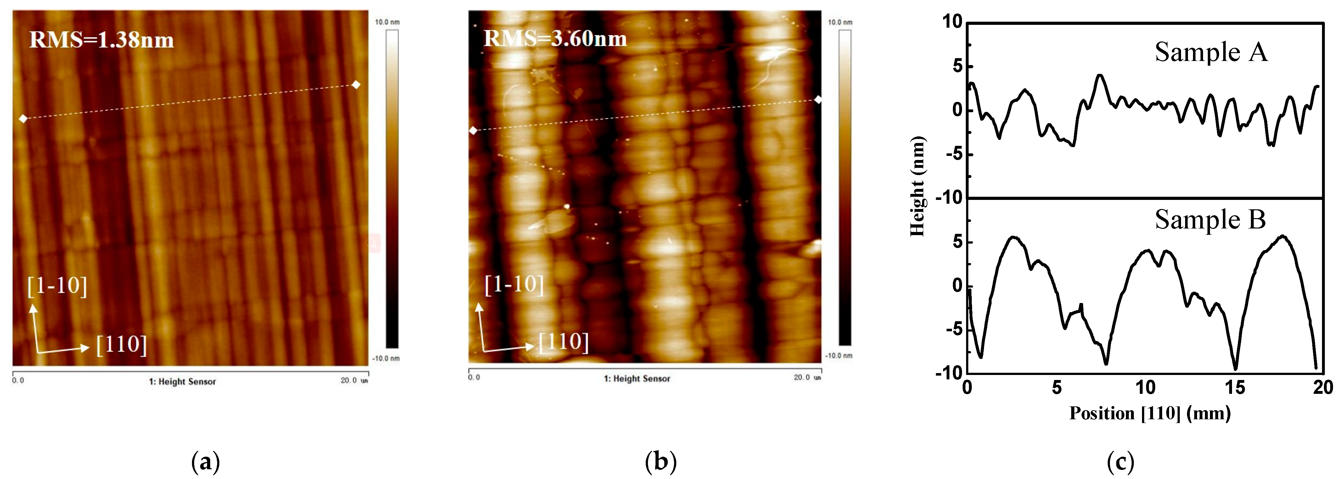
3.1. Surface Morphology

The 20 μm × 20 μm AFM micrographs and related line profiles in [110] direction of two samples are shown in Figure 2. Characteristic undulating morphology with hills and valleys parallel to the intersection of slip planes with the crystal surface, namely, “crosshatch” pattern can be obviously observed. This surface characteristic is typical surface morphology and appeared after plastic strain relaxation in the heteroepitaxy of mismatched zinc-blende structure layers, which means InGaAs is grown in two-dimensional mode with ideal strain relaxation [21]. The root mean square roughness is 1.38 nm and 3.60 nm for sample A and sample B, respectively. Furthermore, the peak-to-valley height of sample B is larger than sample A, as shown in Figure 2c. The results indicate that CUSG structure is better-developed and can smoothen the surface more efficiently, similar conclusion was highlighted [8]. It should be stressed that the thickness of the bottom modulation layer in our case is much thinner. Thinner compositional overshoot could remarkably improve structural and optical properties [22]. In this work, every thin bottom modulation InAsyP1−y layer is compositional overshoot, and lattice is under compressive strain, which should result in hills. However, the thickness does not exceed the critical thickness with respect to the former upper modulation layer, so it provides a relatively flat surface for the following upper modulation layer growth. Under the action of alternatively compressive and tensile strain in CUSG structure, superior surface morphology could be achieved. Therefore, one can conclude that the CUSG structure will provide a better surface morphology relating to higher crystalline quality of the In0.76Ga0.24As layer, and thus lead to a much lower dislocation density and better optical property in sample A.

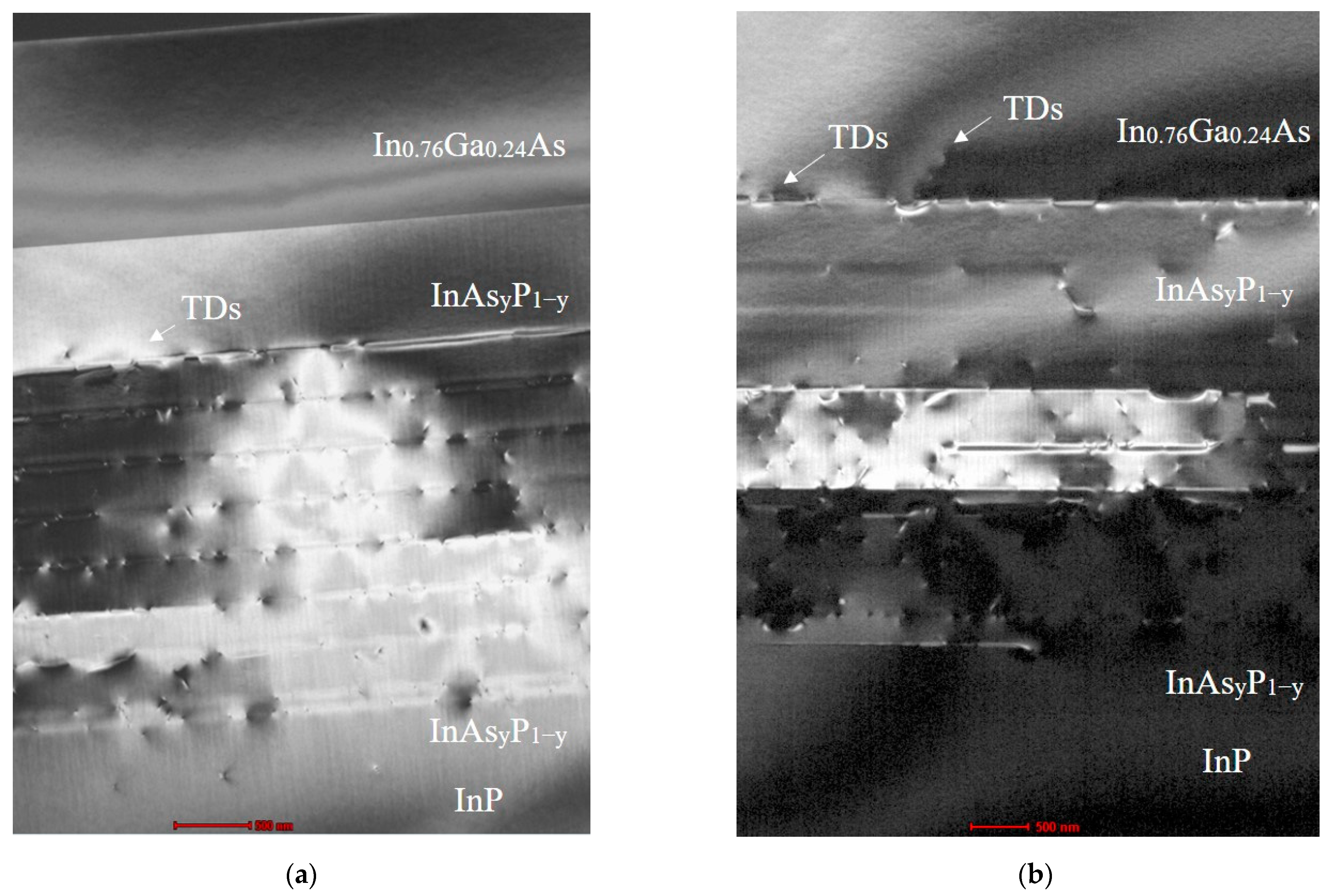
3.2. The Structural Property

The relaxation state of entire III-V epilayers could be characterized by RSMs. According to the research by Hornstra et al. The equivalent bulk lattice mismatch   f can be expressed as [23,24]:
f = ( f f ) 1 υ 1 + υ + f
where f = Δ a a s , and f = Δ a a s are lattice mismatch in the perpendicular and parallel directions, respectively. The υ is the Poisson’s ratio, for In0.76Ga0.24As, υ = 0.34 by using elastic constants of InxGa1−xAs material at 300 K. The strain relaxation of InxGa1−xAs grown on the InP substrate can be described by the following equation [24]:
R = a a s a r e l a x e d a s = f f
where a , and a r e l a x e d represent the in-plane lattice parameters of the epilayer and lattice parameters under completely relaxed state, and a s is the lattice parameters of the substrate.
The RSMs around asymmetric (115) reflection of In0.76Ga0.24As/InP samples were carried out (as shown in Figure 3). Three distinct reciprocal lattice points (RLP) maxima can be found, which corresponded to (i) the InP substrate; (ii) the uppermost InAsP layer of the InAsyP1−y buffers; and (iii) the extended wavelength In0.76Ga0.24As epilayer, respectively. The vertical solid line represents a fully strained and inclined solid line, which is extended to Qx = 0 and represents a fully relaxed epilayer. More information about the lattice parameter could be obtained from the position and the intensity distribution of RSMs. By using Equations (1) and (2), the percentage of strain relaxation is 96.47% and 85.12% for sample A and sample B, respectively, implying that the In0.76Ga0.24As layer and the uppermost InAsP layer almost relaxed completely for sample A. Whereas, residual strain still existed in the uppermost InAsP layer and the In0.76Ga0.24As layer of sample B; therefore, some of threading dislocations may penetrate into the InGaAs layer.
Further investigation into the structural property of the two samples is provided by cross-sectional TEM analysis, as shown in Figure 4, and the In0.76Ga0.24As layer and InAsyP1−y buffer layers are labeled in these figures. Figure 4a shows the sample grown on the CUSG buffers. Misfit dislocations are restricted along with the internal interface, dislocations are significantly decreased in the uppermost InAsP layer, and no threading dislocation is observed in the In0.76Ga0.24As layer of sample A. This mainly benefits from the strain compensation around the interface by the insertion of tensile InAsyP1−y layers, which can change the dislocation glide direction and facilitate the dislocation annihilation, and the interfaces also prevent the threading dislocations from propagating vertically through the structure [25]. It is a reason of the superior surface and better two-dimensional crosshatch pattern in sample A, as illustrated in AFM analysis. Generally speaking, the TDD decreases with a thicker buffer layer [26], so less defects in sample B should appear regarding a ~0.9 μm thicker buffer than that of sample A. However, as shown in Figure 4b, although most of the dislocations are confined within the InAsyP1−y buffers for sample B, there are still some dislocations penetrating the bottom of the InGaAs layer. As no other treatment is applied, it is reasonable to conclude that the residual strain contributes to the penetration of dislocations into the InGaAs layer, which is consistent with the RSMs’ relaxation analysis discussed above. Moreover, it is also clear that the poor surface morphology of sample B is due to the dislocation penetration result of incomplete relaxation [27].

3.3. The Optical Property

The PL spectra of InGaAs epilayer with varying excitation power measured at 10 K are shown in Figure 5. Single band edge peak is observed in sample A, while an additional low-energy shoulder peak appears in sample B. Such asymmetry may be attributed to localized trap states related to structural defects [12]. For the sake of comparison, PL spectra of sample B are deconvoluted using multiple Gaussian curves, and Figure 5b presents excitation power dependence of band edge peak and shoulder peak. It can be seen from that, the band edge peak keeps almost constant with varying excitation power, although an insignificant red-shift with increasing excitation power is shown in sample A. This may be caused by increasing temperature at the measured point, so sample A is probably sensitive to temperature variation. On the other side, the low-energy shoulder in sample B increases from 0.478 eV to 0.486 eV when the excitation power increases from 33 mW to 258 mW, and the slight shift of the shoulder peak is also exhibited in In-rich InxGa1−xAs samples, which is mainly due to defect-related energy band filling effect [12]. In addition, the intensity tends to saturate at high excitation power, which is normally a signature of the localization phenomena for potential fluctuations or carrier transfer in the band-tail [28].
Figure 6a presents PL spectra measured at room temperature for sample A and sample B, and the peak wavelength is 2297 nm and 2302 nm, respectively. An asymmetric line shape with a long high-energy tail and relatively faster declining low-energy edge is displayed for both samples, especially for sample A. This kind of profile is usually explained by a conventional band-to-band transition model, which predominately reflects the density of states of three-dimensional electronic structure and the Boltzmann distribution of carriers or free excitons [29]. Moreover, it is worth mentioning that the intensity of sample A is about 5 times stronger than that of sample B.
Temperature-dependent photoluminescence (TDPL) measurements is also performed from 10 K to 300 K, as shown in Figure 6b. Peak energy shows red shifted when the temperature is higher than 40 K, which is due to band shrinkage effect (thermal activation of carriers). The peak position and the intensity are extracted from those spectra at each temperature.
The relationship between peak energy and temperature can be described by Varshni’s empirical equation as following [30]:
E ( T ) = E ( 0 ) α T 2 T + β
where E(0) is the energy gap at 0 K, α plays the role of T → ∞ limiting value of band-gap shrinkage coefficient, and β is an associated parameter related to the Debye temperature. As mentioned in excitation power-dependent PL, localized states caused by potential fluctuations or carrier transfer in the band-tail may exist. The inhomogeneity of indium composition can result in fluctuation of energy band, thus, an atypical S-shaped behavior of peak energy with temperature will be presented [12]. Unlike the localized states induced S-shaped behavior highlighted in Ref. [12], this work produces good fits to the experimental data for the entire temperature range. The behavior indicates that the distribution of indium composition is homogeneous in the MBE-grown extended wavelength InGaAs material. The fitted equation is also presented in Figure 7, and the Varshni parameter α determined in sample A is higher than that of sample B. A higher α means that sample A is relatively more sensitive with temperature, which is in accordance with the insignificant red-shift with increasing excitation power of sample A [13].
As can also be seen from Figure 6b, the overall intensity of the PL spectra diminishes significantly as temperature increases, which is due to the thermal quenching effect caused by phonon-assisted non-radiative recombination. In order to further understand the mechanism of carrier thermal quenching in the InGaAs layer, Arrhenius-like expression given in Equation (4) is applied to fit the experimental data of the PL intensity [31,32], in which two non-radiative recombination processes are assumed.
I ( T ) = I 0 1 + C 1 e x p ( E a 1 k B T ) + C 2 e x p ( E a 2 k B T )
where T is the measured temperature, I ( T ) is the integrated PL intensity, and k B is Boltzmann’s constant. E a 1 and E a 2 are the thermal activation energy of non-radiative recombination processes. C 1 and C 2 are the ratio of non-radiative to radiative probability for the non-radiative mechanism, in other words, they are related to the density of non-radiative recombination centers.
Figure 8 shows the relationship between intensity and the best fit using Equation (4) with the experimental data, and the activation energy obtained from the fit for each sample are also indicated. The value of E a 1 , which is mainly due to interfacial roughness, is 5.44 meV and 6.24 meV of sample A and sample B, respectively. It indicates that the localized energy caused by interfacial roughness is small. The second process, which is predominant at higher temperatures, mainly results from the suppression of non-radiative recombination centers linked to misfit dislocations, and it is said that higher E a 2 values may be associated with improved internal quantum efficiency [13]. In our case, E a 2 values are 26.67 meV and 38.03 meV for sample A and sample B, respectively. Sample A seems to perform worse at room temperature. In fact, it is effectively the transition probability C2 of the recombination that governs the PL intensity at room temperature [31]. We could see that C2 of sample A is about 5 times smaller than that of sample B, indicating much less misfit dislocation in sample A, in line with the results evidenced in TEM. Hence, stronger PL intensity at room temperature is displayed.

4. Conclusions

Extended wavelength (2.3 μm) InGaAs on common and compositionally undulating step-graded InAsP buffers have been grown by SSMBE, and their structural and optical properties have been investigated by means of AFM, RSM, TEM, and PL measurements. By taking advantage of the strain compensation mechanism, a smaller surface roughness of 1.38 nm, a better relaxation of 96.47%, and fewer dislocations were presented for the sample with improved CUSG buffer structure and thinner buffers. Furthermore, the room-temperature PL intensity of InGaAs grown on a CUSG buffer showed ~5 times stronger than the one grown on a CSG buffer, which could be attributed to less deep non-radiative centers in the In0.76Ga0.24As layer. The emission peak energy with varying temperatures was in good agreement with Varshni’s empirical equation, which implies high crystal quality without inhomogeneity-induced localized states under a low growth temperature. In addition, the InGaAs grown on a CUSG buffer is slightly more sensitive to temperature. To sum up, our work shows that compositionally undulating step-graded InAsP buffers with a thinner bottom modulation layer, grown by SSMBE, is an effective approach to prepare InGaAs materials with wavelengths longer than 2.0 μm and to break the lattice restriction on the materials with even larger mismatch.

Author Contributions

Conceptualization and methodology, X.L. and S.L.; formal analysis and visualization, J.X., T.W., W.Y. and Y.W.; investigation, S.J.; writing original draft preparation, X.L.; writing review and editing, J.X., W.Y. and S.L.; supervision, S.L.; project administration, S.L.; funding acquisition, S.L. All authors have read and agreed to the published version of the manuscript.

Funding

This research was funded by National Key R&D Program, grant number 2018YFB2003305; National Natural Science Foundation of China, grant numbers 61774165, 61875224, 61827823, 61875224 and 61827823; SINANO, grant number Y8AAQ11003; and Vacuum Interconnected Nanotech Workstation, grant number B2006.

Data Availability Statement

The data presented in this study are available within the manuscript.

Acknowledgments

The authors thank Platform for Characterization & Test and Vacuum Interconnected Nanotech Workstation of Suzhou Institute of Nano-Tech and Nano-Bionics (SINANO), Chinese Academy of Sciences (CAS) for the technical support.

Conflicts of Interest

The authors declare no conflict of interest.

References

  1. Nahory, R.; Pollack, M.; Johnston, W.; Barns, R. Band-gap Versus Composition and Demonstration of Vegards Law for In1-xGaxAsyP1-y Lattice Matched to InP. Appl. Phys. Lett. 1978, 33, 659–661. [Google Scholar] [CrossRef]
  2. Kleipool, Q.L.; Jongma, R.T.; Gloudemans, A.M.S.; Schrijver, H.; Lichtenberg, G.F.; van Hees, R.M.; Maurellis, A.N.; Hoogeveen, R.W.M. In-Flight Proton-Induced Radiation Damage to SCIAMACHY’s Extended-Wavelength InGaAs near-Infrared Detectors. Infrared Phys. Technol. 2007, 50, 30–37. [Google Scholar] [CrossRef]
  3. Dai, P.; Lu, S.; Uchida, S.; Ji, L.; Wu, Y.; Tan, M.; Bian, L.; Yang, H. Room-Temperature Wafer Bonded InGaP/GaAs//InGaAsP/InGaAs Four-Junction Solar Cell Grown by All-Solid State Molecular Beam Epitaxy. Appl. Phys. Express 2016, 9, 016501. [Google Scholar] [CrossRef]
  4. Gamel, M.M.A.; Lee, H.J.; Rashid, W.E.S.W.A.; Ker, P.J.; Yau, L.K.; Hannan, M.A.; Jamaludin, M.Z. A Review on Thermophotovoltaic Cell and Its Applications in Energy Conversion: Issues and Recommendations. Materials 2021, 14, 4944. [Google Scholar] [CrossRef] [PubMed]
  5. Wu, Y.; Ji, L.; Dai, P.; Tan, M.; Lu, S.; Yang, H. Effects of Buffer Layer and Back-Surface Field on MBE-Grown InGaAsP/InGaAs Solar Cells. Jpn. J. Appl. Phys. 2016, 55, 022301. [Google Scholar] [CrossRef]
  6. Zhang, J.; Itzler, M.A.; Zbinden, H.; Pan, J.-W. Advances in InGaAs/InP Single-Photon Detector Systems for Quantum Communication. Light Sci. Appl. 2015, 4, e286. [Google Scholar] [CrossRef] [Green Version]
  7. Hudait, M.K.; Brenner, M.; Ringel, S.A. Metamorphic In0.7Al0.3As/In0.69Ga0.31As Thermophotovoltaic Devices Grown on Graded InAsyP1-y Buffers by Molecular Beam Epitaxy. Solid-State Electron. 2009, 53, 102–106. [Google Scholar] [CrossRef]
  8. Ji, L.; Lu, S.L.; Zhao, Y.M.; Tan, M.; Dong, J.R.; Yang, H. Compositionally Undulating Step-Graded InAsyP1-y Buffer Layer Growth by Metal-Organic Chemical Vapor Deposition. J. Cryst. Growth 2013, 363, 44–48. [Google Scholar] [CrossRef]
  9. Ji, L.; Lu, S.-L.; Jiang, D.-S.; Zhao, Y.-M.; Tan, M.; Zhu, Y.-Q.; Dong, J.-R. 0.6-EV Bandgap In0.69Ga0.31As Thermophotovoltaic Devices with Compositionally Undulating Step-Graded InAsyP(1-y)Buffers. Chin. Phys. B 2013, 22, 026802. [Google Scholar] [CrossRef]
  10. Hudait, M.; Lin, Y.; Palmisiano, M.; Ringel, S. 0.6-EV Bandgap In0.69Ga0.31As Thermophotovoltaic Devices Grown on InAsyP1-y Step-Graded Buffers by Molecular Beam Epitaxy. IEEE Electron. Device Lett. 2003, 24, 538–540. [Google Scholar] [CrossRef]
  11. Besikci, C. Extended Short Wavelength Infrared FPA Technology: Status and Trends. In Proceedings of the Quantum Sensing and Nano Electronics and Photonics XV, San Francisco, CA, USA, 28 January–2 February 2018; Razeghi, M., Brown, G., Lewis, J., Leo, G., Eds.; SPIE: Bellingham, WA, USA, 2018; Volume 10540. [Google Scholar]
  12. Smiri, B.; Ben Arbia, M.; Ilkay, D.; Saidi, F.; Othmen, Z.; Dkhil, B.; Ismail, A.; Sezai, E.; Hassen, F.; Maaref, H. Optical and Structural Properties of In-Rich InxGa1-XAs Epitaxial Layers on (100) InP for SWIR Detectors. Mater. Sci. Eng. B-Adv. Funct. Solid-State Mater. 2020, 262, 114769. [Google Scholar] [CrossRef]
  13. Mehdi, H.; Martin, M.; Jany, C.; Virot, L.; Hartmann, J.M.; Da Fonseca, J.; Moeyaert, J.; Gaillard, P.; Coignus, J.; Leroux, C.; et al. Monolithically Integrated InGaAs/AlGaAs Multiple Quantum Well Photodetectors on 300 Mm Si Wafers. AIP Adv. 2021, 11, 085028. [Google Scholar] [CrossRef]
  14. Zhang, Y.-G.; Gu, Y.; Wang, K.; Li, A.-Z.; Li, C. Properties of Gas Source Molecular Beam Epitaxy Grown Wavelength Extended InGaAs Photodetector Structures on a Linear Graded InAlAs Buffer. Semicond. Sci. Technol. 2008, 23, 125029. [Google Scholar] [CrossRef]
  15. Zimmermann, L.; John, J.; Degroote, S.; Borghs, G.; Van Hoof, C.; Nemeth, S. Extended Wavelength InGaAs on GaAs Using InAlAs Buffer for Back-Side-Illuminated Short-Wave Infrared Detectors. Appl. Phys. Lett. 2003, 82, 2838–2840. [Google Scholar] [CrossRef]
  16. Gu, Y.; Zhang, Y.-G.; Li, A.-Z.; Wang, K.; Li, C.; Li, Y.-Y. Structural and Photoluminescence Properties for Highly Strain-Compensated InGaAs/InAlAs Superlattice. Chin. Phys. Lett. 2009, 26, 077808. [Google Scholar]
  17. Hidouri, T.; Saidi, F.; Al-Shahri, B.M. Tuning Spontaneous Emission in BInGaAs/GaAs QWs by Varying the Growth Temperature: Above 1.2 Μm Emission and Solar Cells Application. Opt. Quantum Electron. 2021, 53, 532. [Google Scholar] [CrossRef]
  18. Saidi, H.; Zitouni, O.; Ridene, S. Investigation of Orientation Dependence of Piezoelectric Effects in Strained GaAs/InGaAs Quantum Well Laser. Mater. Sci. Eng. B 2021, 273, 115400. [Google Scholar] [CrossRef]
  19. Gu, Y.; Zhang, Y.G.; Wang, K.; Fang, X.; Li, C.; Zhou, L.; Li, A.Z.; Li, H. Effects of Growth Temperature and Buffer Scheme on Characteristics of InP-Based Metamorphic InGaAs Photodetectors. J. Cryst. Growth 2013, 378, 65–68. [Google Scholar] [CrossRef]
  20. Hudait, M.; Lin, Y.; Palmisiano, M.; Tivarus, C.; Pelz, J.; Ringel, S. Comparison of Mixed Anion, InAsyP1-y and Mixed Cation, InxAl1-XAs Metamorphic Buffers Grown by Molecular Beam Epitaxy on (100)InP Substrates. J. Appl. Phys. 2004, 95, 3952–3960. [Google Scholar] [CrossRef] [Green Version]
  21. Andrews, A.; LeSar, R.; Kerner, M.; Speck, J.; Romanov, A.; Kolesnikova, A.; Bobeth, M.; Pompe, W. Modeling Crosshatch Surface Morphology in Growing Mismatched Layers. Part II: Periodic Boundary Conditions and Dislocation Groups. J. Appl. Phys. 2004, 95, 6032–6047. [Google Scholar] [CrossRef] [Green Version]
  22. Fang, X.; Gu, Y.; Zhang, Y.G.; Zhou, L.; Wang, K.; Li, H.S.B.Y.; Liu, K.H.; Cao, Y.Y. Effects of Compositional Overshoot on InP-Based InAlAs Metamorphic Graded Buffer. J. Infrared Millim. Waves 2013, 32, 481. [Google Scholar] [CrossRef]
  23. Hornstra, J.; Bartels, W. Determination of Lattice-Constant of Epitaxial Layers of III-V Compounds. J. Cryst. Growth 1978, 44, 513–517. [Google Scholar] [CrossRef]
  24. Tseng, M.-C.; Horng, R.-H.; Wuu, D.-S.; Yang, M.-D. Effect of Crystalline Quality on Photovoltaic Performance for In0.17Ga0.83As Solar Cell Using X-Ray Reciprocal Space Mapping. IEEE J. Quantum Electron. 2011, 47, 1434–1442. [Google Scholar] [CrossRef]
  25. He, Y.; Yan, W.; Sun, Y.; Dong, J. Improved Quality of InP Layer on GaAs Substrates by Using Compositionally Modulated Step-Graded AlGaInAs Buffers. J. Mater. Sci. Mater. Electron. 2019, 30, 16251–16256. [Google Scholar] [CrossRef]
  26. Romanov, A.; Pompe, W.; Beltz, G.; Speck, J. Modeling of Threading Dislocation Density Reduction in Heteroepitaxial Layers. I. Geometry and Crystallography. Phys. Status Solidi B-Basic Res. 1996, 198, 599–613. [Google Scholar] [CrossRef]
  27. Ahrenkiel, S.P.; Wanlass, M.W.; Carapella, J.J.; Ahrenkiel, R.K.; Johnston, S.W.; Gedvilas, L.M. Optimization of Buffer Layers for Lattice-Mismatched Epitaxy of GaxIn1−xAs/InAsyP1−y Double-Heterostructures on InP. Sol. Energy Mater. Sol. Cells 2007, 91, 908–918. [Google Scholar] [CrossRef]
  28. Hidouri, T.; Parisini, A.; Ferrari, C.; Orsi, D.; Baraldi, A.; Vantaggio, S.; Nasr, S.; Bosio, A.; Pavesi, M.; Saidi, F.; et al. Combined Impact of B2H6 Flow and Growth Temperature on Morphological, Structural, Optical, and Electrical Properties of MOCVD-Grown B(In)GaAs Heterostructures Designed for Optoelectronics. Appl. Surf. Sci. 2021, 151884, in press. [Google Scholar] [CrossRef]
  29. Su, Z.C.; Xu, S.J.; Wang, R.X.; Ning, J.Q.; Dong, J.R.; Lu, S.L.; Yang, H. Electroluminescence Probe of Internal Processes of Carriers in GaInP Single Junction Solar Cell. Sol. Energy Mater. Sol. Cells 2017, 168, 201–206. [Google Scholar] [CrossRef]
  30. Varshni, Y. Temperature Dependence of Energy Gap in Semiconductors. Physica 1967, 34, 149–154. [Google Scholar] [CrossRef]
  31. Lambkin, J.; Considine, L.; Walsh, S.; Oconnor, G.; Mcdonagh, C.; Glynn, T. Temperature-dependence of the Photoluminescence Intensity of Ordered and Disordered In0.48Ga0.52P. Appl. Phys. Lett. 1994, 65, 73–75. [Google Scholar] [CrossRef]
  32. Zhang, X.; Yang, W.; Xing, Z.; Qiu, H.; Gu, Y.; Bian, L.; Lu, S.; Qin, H.; Cai, Y.; Suzuki, Y.; et al. Investigation of Micromorphology and Carrier Recombination Dynamics for InGaN/GaN Multi-Quantum Dots Grown by Molecular Beam Epitaxy. Crystals 2021, 11, 1312. [Google Scholar] [CrossRef]
Figure 1. (a) Schematic diagram of extended wavelength InGaAs on InP substrate with compositionally undulating step-graded (CUSG) buffer structure (noted as sample A). (b) Schematic diagram of In0.76Ga0.24As on InP substrate with common compositionally step-graded buffer structure (noted as sample B).
Crystals 11 01590 g001
Figure 2. AFM images of extended wavelength InGaAs on InP substrate at a scanning area of 20 μm × 20 μm: (a) sample A (RMS: 1.38 nm); (b) sample B (RMS: 3.60 nm); (c) the line profile along [110] direction of sample A and sample B.
Crystals 11 01590 g002
Figure 3. Asymmetric (115) RSMs of extended wavelength InGaAs on InP substrate: (a) sample A (R = 96.47%); (b) sample B (R = 85.12%).
Crystals 11 01590 g003
Figure 4. Cross-sectional TEM images of extended wavelength InGaAs on InP substrate: (a) sample A and (b) sample B.
Crystals 11 01590 g004
Figure 5. (a) PL spectra of extended wavelength InGaAs on InP substrate measured at 10 K (smoothed): (a) sample A and (b) sample B (the inset is Gaussian decomposition of PL spectrum at 95 mW).
Crystals 11 01590 g005
Figure 6. (a) PL spectra of extended wavelength InGaAs sample at room temperature. (b) PL spectra of extended wavelength InGaAs sample A at different temperatures from 10 K to 300 K (Intensity is plotted in logarithm scale).
Crystals 11 01590 g006
Figure 7. The peak energy of extended wavelength InGaAs on InP substrate as a function of temperature (a) sample A and (b) sample B, the fitting parameters are also given.
Crystals 11 01590 g007
Figure 8. Variation of the normalized integrated PL intensity with the reciprocal temperature for extended wavelength InGaAs on InP substrate. The red solid lines represent the Arrhenius fitting results: (a) sample A; (b) sample B.
Crystals 11 01590 g008
Publisher’s Note: MDPI stays neutral with regard to jurisdictional claims in published maps and institutional affiliations.

