Article

Stabilization of Long-Pitch Supertwisted Nematic Structures

Department of Electrical Engineering, Faculty of Engineering, Sanyo-Onoda City University, Daigakudori 1-1-1, Sanyo-Onoda 756-0884, Japan
*
Author to whom correspondence should be addressed.
Crystals 2021, 11(12), 1541; https://doi.org/10.3390/cryst11121541
Submission received: 10 November 2021 / Revised: 29 November 2021 / Accepted: 7 December 2021 / Published: 9 December 2021
(This article belongs to the Special Issue Liquid Crystal Optics for Applications)

Abstract

:
Stabilized reverse twisted nematic liquid crystal devices (RTN-LCDs) were fabricated using formation of a polymer matrix under UV irradiation with an applied voltage (sustain voltage) in the vicinity of the alignment layers. In the absence of an applied voltage, the non-stabilized RTN structure gradually returns to a splay twist structure. The sustain voltage was decreased with an increase in temperature. A stabilized long-pitch supertwisted nematic (LPSTN) structure could also be formed during the RTN structure stabilization process with a much lower sustain voltage at a temperature near the clearing point. The chiral pitch for the LPSTN structure is longer than that for a typical STN structure. LPSTN-LCDs similar to RTN-LCDs show a large reduction in both the threshold and saturation voltage compared with those for TN-LCDs consisted of the same LC materials. Furthermore, a notable feature of LPSTN-LCDs is a change to a TN structure when a high voltage is applied. A black state can be realized due to the change from the LPSTN structure to the RTN structure unlike the typical STN mode under the crossed nicols condition. In contrast STN-LCDs retain their color due to the retardation because the RTN and LPSTN states are considered topologically equivalent.

Graphical Abstract

1. Introduction

A twisted hybrid aligned [1], hybrid twisted nematic (HTN) [2], hybrid aligned nematic using strong and weak polar anchoring surfaces [3], or reverse twisted nematic (RTN) [4,5,6,7] liquid crystal displays (LCDs) have been proposed to reduce the driving voltage. An HTN that uses strong and weak polar anchoring surfaces was numerically analyzed [8]. Long-pitched supertwisted nematic (LPSTN) LCDs have been reported [9] in the development of RTN-LCDs. In addition, the doping of metallic nanoparticles in the LC system [10], or ferroelectric barium titanate nanoparticles in alignment layer [11] provide low power consumption in the display devices.
The RTN and LPSTN structures were separately formed controlling the chiral pitch to the cell thickness (p/d) ratio [9]. These structures were changed from a splay twisted (ST) structure (Figure 1a), which includes a chiral reagent causing the twist distortion opposite to that determined by the rubbing directions and were formed by the application of voltage over Fredericks transition threshold voltage to the ST structure. The twist of the liquid crystal is basically determined by the angle of the director in the vicinity of the alignment layer depending on the rubbing direction of the alignment layers of the upper and lower substrates. The director of twisted nematic and STN structures, which include a chiral reagent causing the twist distortion that determined by the rubbing directions, rotates in the direction of Azimuth angle. In addition, the STN has a steeper transmittance change than the TN. On the contrary, splay-twisted nemantic structures which include a chiral reagent causing the twist distortion opposite to that determined by the rubbing directions, which rotate in the direction of Azimuth and Polar angles. The RTN and LPSTN structures that include a chiral reagent with the twist distortion opposite to that determined by the rubbing directions have a metastable state and can be maintained when a specific voltage is applied after application of the saturation voltage. This voltage is referred to as the sustain voltage. The ST structure changes to RTN or LPSTN structures as the director near the center of the LC cell is rotated in the opposite direction, as the Gibbs free energy increases with the voltage. This phenomenon can be explained by assuming that the stress of the LC structure generated by the splayed structure with an electric voltage can be released because the reversely twisted structure (no splay deformation) is more stable than the splayed structure [5,12,13]. The RTN structure appears when the p/d ratio is more than three. Moreover, our group has developed a stabilization method for the RTN structure by UV irradiation using reactive mesogens (RMs) with application from 1.25 to 1.5 V [14]. The driving voltage for the RTN-LCD is reduced compared with the TN-LCD (Figure 1). When the p/d ratio is 2.78, the STN structure appears [9]. In the case that the rubbing directions are twisted at 90° by application of high voltage to avoid ST structure, it changes into the RTN structure [5] and, at the same time, the STN structure in which LC material is twisted at 270° could be formed by twisting in the direction opposite to the RTN. These RTN and STN do not contain splayed structures. The p/d value approaches 1.5, which is necessary for the LC to twist 270°; therefore, the ST structure is formed when the voltage is 0 V. Application of a voltage higher than the threshold voltage causes the energy of the ST structure to increase, so that the STN structure is obtained without the splay structure. STN has an increased twist angle from 180° up to 270° [15,16,17], which is known to increase the steepness of the transmittance–voltage curve (V-T curve). In Figure 1, the V-T curve of LPSTN is shown as blue open triangles [9]. When the p/d ratio is 2.14, the RTN structure appears by application of a high voltage (metastable state 2 (ii) in Figure 1d), while the typical STN (p/d ratio is 1.5) does not change to RTN. Our group has termed this non-typical STN (p/d ratio more than 1.5) LPSTN.
In this study, we focus on the effect of thermal energy and attempt to cause transformation by heat instead of voltage to maintain the structure by application of a low voltage because, by reducing the applied voltage, RTN-LCDs of high transmittance without applied voltage can be obtained. Transformation from the ST state to the RTN state occurred at a temperature slightly below the nematic–isotropic (NI) point with the application of 1.0 V. Furthermore, the electro–optical properties and Gibbs free energy were calculated for each structure and compared with the obtained results. The Gibbs free energy is calculated by Frank–Oseen free energy density F 1 and the energy per unit volume by electric field F 2   F 1 is given by:
F 1 = 1 2 K 11 ( · n ^ ) 2 + 1 2 K 22 ( n ^ · × n ^ + q 0 ) 2 + 1 2 K 33 ( n ^ × × n ^ ) 2
where K11, K22 and K33 are elastic constants for different director deformations: splay, twist and bend, respectively, q 0 = 2 π / P 0 is constant and describes the chiral pitches P 0 of the helix, and n ^ is eigenvector [18]. F 2 is given by:
F 2 = 1 2 ε E · E
where ε is the dielectric tensor of the liquid crystal, and E is the electric field. The Gibbs free energy G can be expressed by:
G = F 1 F 2

2. Materials and Methods

The LC material MLC-2173 (US048) (Merck & Co. Inc., Darmstadt, Germany) had a left-handed pitch of 15.0 µm and MJ141067 (US048) had 5 wt% RM in MLC-2173 (US048). Two LC were mixed to be 1 wt% RM. The MLC-2173 has positive dielectric anisotropy (20.8). The polyimide material for the alignment layers was produced by mixing PIA-X768-01X and PIA-X359-01X (Chisso Petrochemical Corp., Tokyo, Japan) in a 15:85 ratio. The pretilt angle of the alignment layer was confirmed to be 6° with a pretilt analysis system (PAS-301, Elsicon Inc., Newark, NJ, USA). The cell thicknesses were set at 5.0 and 5.4 µm using silica bead spacers. The rubbing directions were set to form a right-handed twist of the LC material without a chiral reagent from the upper to the lower substrate. A splayed twisted structure was formed when left-handed LC materials were injected into the cell. The temperature was controlled with a high-precision temperature controller (mK1000, Instec Inc., Boulder, CO, USA) and UV light was irradiated to cure the RM with a UV lamp (LUV-6, AS ONE Co., Osaka, Japan). The electro-optical properties (applied voltage dependence of the transmittance and response time) were measured using OPTIPRO-standard (Shintech Inc., Yamaguchi, Japan). The optical axis of one polarizer was set parallel to one of the rubbing directions in a crossed nicols setting. The elastic constant was measured with an elastic constant measurement system (EC-1, Toyo Corp., Tokyo, Japan). Simulations of the electro-optical properties and Gibbs free energy were performed using LCD Master (Shintech Inc.) software under various conditions, such as pretilt angle, cell thickness, and chiral pitch. The LCDs were driven by a 1 kHz square wave.

3. Results and Discussions

The transition from ST to RTN was confirmed by polarized optical microscopy (POM) measurements under a crossed nicols condition. The clearing point for this LC is 353 K. Figure 2 shows the lowest sustain voltage for each cell thickness as a function of temperature. These voltages started to decrease near 343 K. Transition to the isotropic phase occurred with application of 1.0 V at 354.7 and 356.5 K for the cell thicknesses of 5.0 and 5.4 µm, respectively. The chiral pitch extended up to 16.8 µm at high temperature, as shown in Figure 3. The chiral pitch was once saturated near 343 K; however, it extended up to 16.8 µm at high temperature, as shown in Figure 3. The change of the molecular conformation of chiral reagent could occur at high temperature. The change of the pitch dependence on temperature could be explained by the change of the molecular conformation [19]. Therefore, the disturbance of the chiral pitch on temperature could be explained by the large change of the conformation of the chiral reagent. Although the reason is not stated, there are reports that the chiral pitch changed twice at high temperatures [20].
The ST structure changed to the RTN structure with application of 1.2 V (transition voltage) at 356 K. A decrease in the voltage to 0.5 or 0 V resulted in a transition of the RTN structure to the ST structure via the STN state in Figure 4a,b. Transition speed to STN is faster than that to ST. At this time, the STN structure changed to the RTN structure with application of 1.0 V, while the ST structure was maintained. After a relatively long time of applying a voltage lower than 1.0 V, the structure becomes the ST structure (Figure 4c). It is necessary to apply 1.2 V to transform the ST structure into the RTN structure, while 1.0 V is required for a transition from the STN to RTN structure (Figure 4d). Therefore, there is a higher potential barrier between ST and RTN than that between STN and RTN.
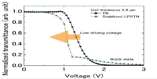
These RTN-LCDs were irradiated with UV light for 1 h, while 1.0 V was applied at 356 K, after confirmation of the RTN structure with POM. After UV irradiation, the RTN structure was maintained at high temperature; however, the LPSTN structure was formed at room temperature when the cell thickness was 5.4 µm. Figure 5 (green solid triangles) shows V-T curves for the LPSTN structure. On the other hand, when the cell thickness was 5.0 µm, the RTN structure at high temperature relaxed to the ST structure at room temperature even after UV irradiation. The driving voltage increased in the order of RTN-LCD < LPSTN-LCD < TN-LCD. When the V-T curves of STN-LCD were calculated (LCD Master) for cell thicknesses of 5.0–6.2 µm with a chiral pitch of 15 µm, a pretilt of 6° and a twist angle of 270°, the driving voltage was high as a function of thickness (Figure 6). Figure 7 shows V-T curves calculated for various chiral pitches of 10–25 µm with a chiral pitch of 15 µm, a pretilt of 6°, a twist angle of 270°, and a cell thickness of 5.4 µm. A longer chiral pitch results in a lower driving voltage; however, if the pitch is too long (chiral pitch is 25 µm), then the transmittance slowly decreases as a function of the voltage. Although the transmittance of LPSTN did not decrease to zero at 1.2 V in Figure 5, the steepness of transmittance increased compared with the TN or RTN. In addition, the transmittance decreased to zero in simulation in the case of the cell thickness of 5.4 μm and chiral pitch of 20 μm. Therefore, we thought that a black state at low driving voltage can be realized by controlling condition of LCD.
The transmittance and the change of azimuth angle dependence on voltage were calculated for LPSTN using LCD Master for a cell thickness of 5.4 µm and a chiral pitch of 15 µm, and the results are shown in Figure 8 and Figure 9. The transmittance decreased similar to that for STN LCDs until 1.06 V and then dropped slowly from 1.07 V. The twist of the azimuth angle was 270° up to 1.06 V and then changed to 90°, which is not simple rotation. The LC molecules near the alignment layer twist left-handed where z/d implies the normalized thickness is from 0.0 to 0.4 and from 0.6 to 1.0 and those near the center of the cell twist right-handed at more than 90°. This phenomenon is an intrinsic twist for the RTN structure. Consequently, the LPSTN structure changed into an RTN structure with application over a certain voltage.
The chiral pitch is known to cause length increase, and the decrease in physical properties (e.g., the dielectric constant anisotropy, and the elastic constant) under heating. The chiral pitch was elongated to 16.8 μm (Figure 3) and the physical properties changed (Table 1) at 353 K. The physical properties at 353 K were estimated from multiplying nominal values at room temperature (298 K) by the ratio of measured values at 298 K to measured values at 353 K. The tilt angle in the vicinity of the alignment layer may be lower than that in the previous study [14], because the sustain voltage is low. The pretilt angle for LCDs has been reported to be controllable by polymer matrix formation in the vicinity of the alignment layers by application of an electric voltage [14,21,22].
The pretilt angle was assumed 15° because the RTN structure was maintained by UV irradiation with application of 1 V, while the pretilt angle is 6.0° for MLC-2173 without chiral dopant and RM at room temperature. The Gibbs free energy for RTN and LPSTN was calculated for the difference of (i) the physical properties (Figure 10a,b), and (ii) the pretilt angles under the condition (i) (Figure 10c,d).
At the beginning, the Gibbs free energy of the RTN and LPSTN structure at high temperature decreased at 0 V compared with the Gibbs free energy of those structures at room temperature (Figure 10a,b). Additionally, these energies then slowly decreased as a function of voltage. The transition voltage from LPSTN structure (blue inverted triangles) to RTN structure (green triangles) under the physical properties at 353 K was lower than the transition voltage from LPSTN structure (black squares) to RTN structure (red circles) at 298 K. Secondly, the transition voltage from LPSTN structure (sky blue diamonds) to RTN structure (purple left-pointing triangles) was lower than the transition voltage from LPSTN structure (blue inverted triangles) to RTN structure (green triangles) in Figure 10c,d. For application of 1.0 V, the RTN structure was stable because the LPSTN structure changed to the RTN structure, even if the pretilt angle was kept low.
For the RTN structure with the application of 1 V at 356 K experimentally, two routes are conceivable for the process of decreasing the voltage from 1 to 0 V; (i) the RTN remaining (green triangles in Figure 11) or (ii) the RTN changing to the LPSTN at 0.95 V (blue inverted triangles in Figure 11). The LPSTN structure was observed to change to the RTN structure with the application of 1.0 V at 356 K in Figure 4. Therefore, the RTN structure when polymerized with the application of 1 V at 356 K was the RTN structure that was changed from the LPSTN. After being polymerized, the LPSTN structure was stable at room temperature.
A notable point of the STN-LCD is that their sharper threshold properties can realize a larger number of pixels in the case of passive matrix LCDs. For multiple-line addressing of passive matrix LCDs, the sharpness of the threshold property can be expressed by:
α = V s a t V t h
where Vsat is the saturation voltage and Vth is the threshold voltage. A sharper threshold property means that α approaches one more closely. The maximum number of scanning electrodes of passive matrix addressing Nmax, can be expressed using α [23].
N m a x = { α 2 + 1 α 2 1 } 2
In the case where α approaches one, the possible number of scanning electrodes increases. For this reason, high-resolution LCDs can be achieved using the sharp threshold property of the STN mode. However, because the STN mode uses the change in the retardation of liquid crystals, it has a problem in that the transmitted light is colored. An LPSTN LCD possesses the STN structure without an applied voltage and exhibits the sharp threshold property. However, when voltage larger than the threshold voltage is applied, it changes to the RTN-LCD structure and shows the black state without color. Therefore, an LPSTN can realize the sharp threshold property of the STN mode and the black state without the color of the TN mode.
The change from LPSTN to RTN occurs because the RTN and LPSTN states are considered topologically equivalent. The LPSTN mode showing low driving voltage and a realizing black state could be an improved alternative candidate for STN-LCDs.

4. Conclusions

An increase in the temperature decreased the voltage for the ST to RTN structural transition and the sustain voltage for the RTN structure. The LPSTN-LCD but not the RTN-LCD was successfully stabilized with UV irradiation near the clearing point. The differences between this study and previous studies are the temperature during UV irradiation and the cell thickness. The notable points of the LPSTN-LCD are a low driving voltage and a black display when a high voltage is applied under the crossed nicols condition. Due to the change from the STN structure to the TN structure, a black state can be realized, unlike the typical STN mode under the crossed nicols condition. The lower limit of the p/d ratio for the LPSTN was 2.14 in 2012; however, that was improved to 2.78 using this method. A lower driving voltage was calculated for chiral pitches of 15 or 20 μm and cell thicknesses of 5.0 or 5.4 μm (p/d ratios of 3.0 or 3.7). The structure was returned to the ST structure under p/d ratio of 3.0. If the p/d ratio is dominant, then the structure will be returned with p/d ratio of 3.7.

Author Contributions

M.I. proposed the devices and wrote the manuscript. K.T. supervised. S.O. prepared the sample cells and made measurements. All authors have read and agreed to the published version of the manuscript.

Funding

This research received no external funding.

Institutional Review Board Statement

Not applicable.

Informed Consent Statement

Not applicable.

Data Availability Statement

Not applicable.

Acknowledgments

The authors are thankful to Merck & Company Incorporated for providing the LC materials, and to Chisso Petrochemical Corporation for providing the polyimide materials. This work was supported by the Organization for Research Promotion Sanyo-Onoda City University.

Conflicts of Interest

The authors declare no conflict of interest.

References

  1. Kim, Y.J.; Lee, S.-D. Reflective Mode of a Nematic Liquid Crystal with Chirality in a Hybrid Aligned Configuration. Appl. Phys. Lett. 1998, 72, 1978–1980. [Google Scholar] [CrossRef]
  2. Kubono, A.; Kyokane, Y.; Akiyama, R.; Tanaka, K. Effects of Cell Parameters on the Properties of Hybrid Twisted Nematic Displays. J. Appl. Phys. 2001, 90, 5859–5865. [Google Scholar] [CrossRef]
  3. Yamaguchi, R.; Sakamoto, Y. Homogeneous-Twisted Nematic Transition Mode Liquid Crystal Display by out-of-Plane Field. In Proceedings of the International Display Workshops (IDW’17), Sendai, Japan; 2017; Volume 24, pp. 294–295. Available online: https://researchmap.jp/read0188761/published_papers/19822221 (accessed on 9 December 2021).
  4. Takatoh, K.; Kaneko, T.; Uesugi, T.; Kobayashi, S. New Approach to Reduce the Driving Voltage for TN-LCDs. In Proceedings of the International Display Workshop (IDW’07), Sappro, Japan; 2007; Volume 14, pp. 421–424. Available online: https://www.jstage.jst.go.jp/article/ekitou/2007/0/2007_0_103/_pdf/-char/ja (accessed on 9 December 2021).
  5. Takatoh, K.; Akimoto, M.; Kaneko, H.; Kawashima, K.; Kobayashi, S. Molecular Arrangement for Twisted Nematic Liquid Crystal Displays Having Liquid Crystalline Materials with Opposite Chiral Structures (Reverse Twisted Nematic Liquid Crystal Displays). J. Appl. Phys. 2009, 106, 064514. [Google Scholar] [CrossRef]
  6. Takatoh, K.; Uno, H.; Taniguchi, H.; Watanabe, I. Stable Reverse TN-LCDs (RTN) Using High Pretilt Angle Alignment Layers. In Proceedings of the International Display Workshops (IDW’16), Fukuoka, Japan; 2016; Volume 23, pp. 3–7. Available online: https://jglobal.jst.go.jp/en/detail?JGLOBAL_ID=202102285281164373 (accessed on 9 December 2021).
  7. Takatoh, K.; Watanabe, I.; Yonezawa, Y.; Goda, K. The Novel TN LCD of the Lowest Driving Voltage. In Proceedings of the International Display Workshops (IDW’18), Nagoya, Japan; 2018; Volume 25, p. 211. Available online: https://www.idw.or.jp/IDW18AP.pdf (accessed on 9 December 2021).
  8. Yamaguchi, R.; Kawata, S. Ultra-Low Driving Voltage in Quasi-Twisted Nematic Mode Using Weak/Strong Anchoring Hybrid Alignment Surface. In Proceedings of the International Display Workshops (IDW’20), Virtual, Japan; 2020; Volume 27, pp. 131–132. Available online: https://confit.atlas.jp/guide/event-img/idw2020/LCTp2-04/public/pdf_archive?type=in (accessed on 9 December 2021). [CrossRef]
  9. Akimoto, M.; Minami, S.; San-No-Miya, M.; Kobayashi, S.; Takatoh, K. Different p/d Ratios Lead to Different Twisted LC Configurations in Reverse Twisted Nematic LCD. In Proceedings of the International Display Workshops (IDW’11), Nagoya, Japan; 2011; Volume 3, pp. 1593–1596. Available online: https://www.researchgate.net/publication/289406160_Different_pd_ratios_lead_to_different_twisted_LC_configurations_in_reverse_twisted_nematic_LCD (accessed on 9 December 2021).
  10. John, V.N.; Shiju, E.; Arun, R.; Ravi Varma, M.K.; Chandrasekharan, K.; Sandhyarani, N.; Varghese, S. Effect of Ferroelectric Nanoparticles in the Alignment Layer of Twisted Nematic Liquid Crystal Display. Opt. Mater. 2017, 67, 7–13. [Google Scholar] [CrossRef]
  11. SJ, S.; Gupta, R.K.; Kumar, S.; Manjuladevi, V. Enhanced Electro-Optical Response of Nematic Liquid Crystal Doped with Functionalised Silver Nanoparticles in Twisted Nematic Configuration. Liq. Cryst. 2020, 47, 1678–1690. [Google Scholar] [CrossRef]
  12. Takatori, K.-I.; Sumiyoshi, K. Splayed TN Configuration Stability in Domain-Divided TN Mode. Mol. Cryst. Liq. Cryst. Sci. Technol. Sect. A Mol. Cryst. Liq. Cryst. 1995, 263, 445–458. [Google Scholar] [CrossRef]
  13. Saito, Y.; Takano, H.; Chen, C.J.; Lien, A. Stability of UV-Type Two-Domain Wide-Viewing-Angle Liquid Crystal Display. Jpn. J. Appl. Phys. 1997, 36, 7216. [Google Scholar] [CrossRef]
  14. Takatoh, K.; Watanabe, I.; Goda, K. Stabilisation of Reverse Twisted Nematic Structure by Forming Polymer Matrix in the Vicinity of the Alignment Layer. Liq. Cryst. 2020, 47, 1–5. [Google Scholar] [CrossRef]
  15. Scheffer, T.J.; Nehring, J. A New, Highly Multiplexable Liquid Crystal Display. Appl. Phys. Lett. 1984, 45, 1021–1023. [Google Scholar] [CrossRef]
  16. Li, J.; Lee, E.S.; Vithana, H.; Bos, P.J. Super-Twisted-Nematic Liquid Crystal Displays with Multi-Domain Structures. Jpn. J. Appl. Phys. 1996, 35, L1446. [Google Scholar] [CrossRef]
  17. Scheffer, T.; Nehring, J. Supertwisted Nematic (Stn) Liquid Crystal Displays. Annu. Rev. Mater. Sci. 1997, 27, 555–583. [Google Scholar] [CrossRef]
  18. Frank, F.C.I. Liquid Crystals. On the Theory of Liquid Crystals. Discuss. Faraday Soc. 1958, 25, 19–28. [Google Scholar] [CrossRef]
  19. Huff, B.P.; Krich, J.J.; Collings, P.J. Helix Inversion in the Chiral Nematic and Isotropic Phases of a Liquid Crystal. Phys. Rev. E 2000, 61, 5372–5378. [Google Scholar] [CrossRef] [PubMed] [Green Version]
  20. Shim, K.S.; Heo, J.U.; Jo, S.I.; Lee, Y.-J.; Kim, H.-R.; Kim, J.-H.; Yu, C.-J. Temperature-Independent Pitch Invariance in Cholesteric Liquid Crystal. Opt. Express OE 2014, 22, 15467–15472. [Google Scholar] [CrossRef] [PubMed]
  21. Lu, L.; Sergan, V.; Bos, P.J. Mechanism of Electric-Field-Induced Segregation of Additives in a Liquid-Crystal Host. Phys. Rev. E Stat. Nonlin Soft Matter Phys. 2012, 86, 051706. [Google Scholar] [CrossRef] [PubMed] [Green Version]
  22. Sergan, V.; Sergan, T.A.; Bos, P.J.; Lu, L.; Herrera, R.; Sergan, E.V. Control of Liquid Crystal Alignment Using Surface-Localized Low-Density Polymer Networks and Its Applications to Electro-Optical Devices. J. Mol. Liq. 2018, 267, 131–137. [Google Scholar] [CrossRef]
  23. Lueder, E. Liquid Crystal Displays: Addressing Schemes and Electro-Optical Effects; Wiley: Hoboken, NJ, USA, 2001. [Google Scholar]
Figure 1. Schematic diagrams of LC structures; (a) initial state, ST; (b) metastable state 1, RTN; (c) metastable state 2a, LPSTN; (d) metastable state 2b, RTN. The ST structure changed to the metastable state (b) RTN or (c) LPSTN by high voltage application when the p/d ratio was 3.0 or 2.14. (e) Dependence of transmittance on the applied voltage for TN-LCDs (cell thickness of 5.0 µm), RTN-LCDs (chiral pitch of 15.0 µm, cell thickness of 5.0 µm, RM), and LPSTN-LCD (chiral pitch of 15.0 µm, cell thickness of 7.0 µm) [9,14]. Solid symbols indicate MLC-2173 and open symbols indicate ZLI-4792.
Crystals 11 01541 g001
Figure 2. Sustain voltage for RTN structure as a function of temperature for cell thicknesses of 5.0 (red solid circles) and 5.4 µm (black solid squares). The insert shows an enlarged view of the high temperature region.
Crystals 11 01541 g002
Figure 3. Chiral pitch length as a function of temperature.
Crystals 11 01541 g003
Figure 4. POM images acquired at 356 K; (a) immediately after changing the applied voltage from 1.2 to 0.5 V, (b) after a short time, and (c) after a relatively long time. (a) The structure changed from RTN to STN or ST. (b) The transition speed to STN was faster than that to ST. At this time, increasing the applied voltage to 1.0 V results in transition of the STN structure to the RTN structure, while the ST structure is maintained. (c) After a relatively long time of applying a voltage lower than 1.0 V, the structure eventually becomes the ST structure. (d) The ST structure changed to the RTN structure with application of 1.2 V at 356 K. A decrease in the voltage to 0.5 or 0 V resulted in a transition of the RTN structure to the ST structure via the STN state. The STN structure changed to the RTN structure with application of 1.0 V at 356 K.
Crystals 11 01541 g004
Figure 5. Transmittance as a function of applied voltage for TN (black solid pentagons, cell thickness of 5.4 μm), LPSTN (green solid triangles, chiral pitch of 15.0 µm, cell thickness of 5.0 µm, RM), TN (black solid squares, cell thickness of 5.0 μm), and RTN (red solid circles, chiral pitch of 15.0 µm, cell thickness of 5.0 µm, RM).
Crystals 11 01541 g005
Figure 6. Transmittance as a function of the applied voltage for LPSTN (MLC-2173, chiral pitch 15.0 μm) with cell thicknesses of 5.0, 5.4, and 6.2 μm. The threshold and saturation voltage decreased with the cell thickness.
Crystals 11 01541 g006
Figure 7. Transmittance as a function of applied voltage for LPSTN with chiral pitches of 5, 10, 15, 20, and 25 μm. Open symbols indicate simulation data and solid symbols show measurement data.
Crystals 11 01541 g007
Figure 8. Transmittance as a function of the applied voltage for LPSTN (MLC-2173, chiral pitch 15.0 μm, cell thickness 5.4 μm).
Crystals 11 01541 g008
Figure 9. Azimuth angle dependence of the normalized cell thickness for LPSTN (MLC-2173, chiral pitch 15.0 μm, cell thickness 5.4 μm). The angle is 270° until the applied voltage is 1.06 V and 90° over 1.07 V. The z/d implies normalized thickness.
Crystals 11 01541 g009
Figure 10. Gibbs free energy for the RTN and the LPSTN structures with a cell thickness of 5.5 μm (a) at 298 K or those at 353 K (c) at 353 K with a pretilt angle of 6° or 15° (lower left), and (b,d) enlarged views of the left-hand panels near 1 V.
Crystals 11 01541 g010
Figure 11. There are two routes from the RTN structure with application of 1 V at 353 K; (i) the RTN structure remaining, or (ii) changing to the LPSTN structure at low voltage.
Crystals 11 01541 g011
Table 1. Dielectric constant anisotropies and elastic constants were measured at 298 and 355 K. The estimated value was calculated by dividing the nominal value by the ratio of measured values at 298 K to the measured values at 355 K.
Δε(F/m)K11(pN/m2)K22(pN/m2)K33(pN/m2)
measured value@298 K15.62.410.520.5
measured value@353 K3.90.62.64.3
nominal value@298 K20.88.718.113.3
estimated value@353 K5.22.24.52.8
Publisher’s Note: MDPI stays neutral with regard to jurisdictional claims in published maps and institutional affiliations.

