Article

Numerical Modeling of High Conversion Efficiency FTO/ZnO/CdS/CZTS/MO Thin Film-Based Solar Cells: Using SCAPS-1D Software

1
Department of Mathematics and Sciences, Ajman University, Ajman P.O. Box 346, United Arab Emirates
2
Nonlinear Dynamics Research Center (NDRC), Ajman University, Ajman P.O. Box 346, United Arab Emirates
3
School of Physics, Universiti Sains Malaysia (USM), Penang 11800, Malaysia
4
Department of Chemistry, An-Najah National University, Nablus P400, Palestine
5
Department of Chemistry, University of Calicut, Kerala 673635, India
6
College of Pharmacy & Health Sciences, Ajman University, Ajman P.O. Box 346, United Arab Emirates
7
Centre of Medical and Bio-Allied Health Sciences Research, Ajman University, Ajman P.O. Box 346, United Arab Emirates
*
Author to whom correspondence should be addressed.
Crystals 2021, 11(12), 1468; https://doi.org/10.3390/cryst11121468
Submission received: 6 November 2021 / Revised: 22 November 2021 / Accepted: 24 November 2021 / Published: 26 November 2021

Abstract

:
The numerical modeling of a copper zinc tin sulfide (CZTS)-based kesterite solar cell is described in detail in this article. To model FTO/ZnO/CdS/CZTS/MO structured solar cells, the Solar Cell Capacitance Simulator-one-dimension (SCAPS-1D) program was utilized. Numerical modeling was used to estimate and assess the parameters of various photovoltaic thin film solar cells. The impact of different parameters on solar cell performance and conversion efficiency were explored. Because the response of a solar cell is partly determined by its internal physical mechanism, J-V characteristic characteristics are insufficient to define a device’s behavior. Regardless of the conviction in solar cell modeling, variable attributes as well as many probable conditions must be handled for simulation. Promising optimized results were obtained with a conversion efficiency of ( η % = 25.72%), a fill factor of (FF% = 83.75%), a short-circuit current of ( J S C   = 32.96436 mA/cm2), and an open-circuit voltage of ( V O C = 0.64 V). The findings will aid in determining the feasibility of manufacturing high-efficiency CZTS-based solar cells. First, in the SCAPS-1D environment, the impacts of experimentally constructed CZTS solar cells were simulated. The experimental data was then compared to the simulated results from SCAPS-1D. After optimizing cell parameters, the conversion efficiency of the improved system was observed to rise. The influence of system factors, such as the thickness, acceptor, and donor carrier concentration densities of the absorber and electron transport layers, and the effect of temperature on the efficiency of CZTS-based photovoltaic cells, was explored using one-dimensional SCAPS-1D software. The suggested findings will be extremely useful to engineers and researchers in determining the best method for maximizing solar cell efficiency, as well as in the development of more efficient CZTS-based solar cells.

1. Introduction

Solar cells have evolved as a more modern and comparatively renewable energy source that, when generated on a larger scale, is both environmentally beneficial and cost effective. Photovoltaic devices with excellent power conversion efficiency and negligible material deterioration are currently being researched for energy generation [1]. For many years, silicon-based solar cells conquered the market. Advanced fabrication processes are required for the fabrication and delivery of silicon-based solar cells, which raises the cost of the solar panel [2]. The fundamental benefit of solar devices is that they deliver low-cost, long-lasting, and environmentally benign energy by utilizing highly scalable and adaptable organic-polymer materials. However, several factors, such as degradation processes generated by air exposure, humidity, ultraviolet radiation, water, and heat, contribute to the decline in their energy efficiency and longevity [3]. As manufacturing skills increase, thin film solar cells are becoming increasingly prevalent. Thin film technology is a major area of research in the photovoltaic industry since it is one of the most cost-effective and efficient techniques for generating solar cells. Thin film technology is less expensive than other technologies since it employs fewer materials and is based on a variety of light-absorbing semiconductors [4]. Kesterite solar cells based on CZTS and related alloys are a possible alternative to chalcopyrite absorbers [5,6,7]. The CZTS’s strong optical and electrical characteristics, including an optical band gap of 1.4 eV to 1.5 eV and a significant absorption coefficient of 104 cm−1, have made it a fascinating insight for the thin film community [8]. On the earth, the kestkesterite solar cell absorber (CZTS) is a prevalent material [9]. The sulfur-based kestkesterite solar cell absorber (CZTS), in particular, has the potential to deliver a significant amount of energy at a low cost due to the abundance of raw materials. Because selenium is present in the lattice, its selenium-based counterpart (CZTSe) is less common. Kesterite solar cells may be made as roll-to-roll modules from powders or as extremely thin film layers, allowing them to be employed in applications where weight and flexibility are crucial. However, there are still issues to be addressed, such as the solar cells’ lower efficiency when compared to competitors Cu(In,Ga)(S,Se)2 and CdTe [10], as well as the solar cells’ dependability, which must be able to last more than 20 years. According to the Shockley–Queisser limit, a CZTS-based solar cell can potentially attain an optimal conversion efficiency of roughly 28% by tuning the band gap. However, it is not experimentally viable to attain 28% conversion efficiency from a solar cell due to a lack of understanding of device properties [11]. Numerical modeling can play a major part in a deeper understanding of system characteristics by modelling various device architectures, which can save time and money. Computational modeling was used in this study to estimate and analyze the influence of physical parameters on system output, such as absorber thickness and doping concentration, buffer and window layers, and temperature effect. The unit was modeled using the modeling application “Solar Cell Capacitance Simulator” (SCAPS-1D). To begin, a basic heterostructure for CZTS/CdS/ZnO thin films was investigated, with molybdenum (MO) serving as the back contact and indium tin oxide (ITO) serving as the front contact. Solar cell performance was shown to be influenced by variations in absorber thickness, doping concentration, and working temperature after analysis. First, the SCAPS-1D system was used to mimic the impacts of experimentally constructed CZTS solar cells. The experimental results were then compared to the results of the SCAPS-1D simulation. The research’s key goals and objectives are to apply computational modeling to enhance thin film solar cell performance, to suggest new approaches to increase the efficiency of experimental solar cells, and to develop alternative strategies to lower thin film solar cell costs. The effects of the absorber, buffer, and window layers’ thickness, doping concentration, and working temperature, as well as the working temperature, on the cell performance were explored.

2. Numerical Modeling and Material Parameters

Numerical modeling is a technique for analyzing system behavior with the use of sophisticated mathematical models and aids in the development of analytical solutions. Numerical analysis may be particularly valuable in the production and fabrication of effectively performing semiconductor-based solar modules. The integration of real-life issues with virtual machine settings is the highest priority goal of numerical modeling techniques implementation for design engineers and researchers [12], as they seek the most optimum and effective approaches to handle a complicated challenge. Academic institutions and universities prioritize computer-based learning methodologies because real-world design challenges may be handled in computer-based testing environments without requiring physical or functional implementation. Fundamental physical parameters such as the concentration of holes and electrons, as well as the electrical potential, are calculated using modeling approaches. It also provides greater details on how material physical properties influence system functional parameters or attributes. For numerical modeling of solar cells, physical material properties are utilized as inputs to simulation software [13]. To translate genuine or actual device J-V characteristics and functional parameters, such as quantum conversion performance, fill factor, short circuit current, and open circuit voltage, into device modeling, experimental data is required. Numerical simulation enables a more in-depth and simple knowledge of system behavior. To acquire a better understanding of a device’s output, simulation software must be able to solve semiconductor fundamental equations, including the continuity equation for holes and electrons and the Poisson equation linking charge to electrostatic potential.

2.1. Numerical Modeling

Current flow is caused by electrons and holes moving in opposing directions. The number of electrons and holes in a molecule is the same. The electron mobility μe is almost double that of the hole mobility μp [14]. Equation (1) gives the overall flow of current density ( J ) owing to electron and hole flow.
J = n i e ( μ e + μ p ) E
μ e and μ p are the electron and hole mobilities (cm2/Vs), n i and p i are free electrons densities in an intrinsic semiconductor (cm−3), e is the elementary charge (1.6 × 10⁻¹⁹ C), and E is the applied electric field (V/m).
The conductivity of a semiconductor is determined by the quantity of current carriers present per unit volume and the current carriers themselves. With a rise in temperature, n i and p i increase, and the intrinsic semiconductor conductivity increases, implying that resistance decreases. The main properties of the forward and reverse biasing zones of diodes are explained by Shockley’s equation [15]. Equation (2) gives the diode current equation.
I = I o ( e q V D n k T 1 )
where   I represents diode current, Io represents reverse saturation current, V D represents diode voltage, n represents ideality factor, k represents Boltzmann’s constant (1.38 × 10⁻²³ J/K), and T represents absolute temperature (K). When zero load (at   R L = 0 ), or short-circuit current (Isc) at the voltage of a solar cell, the maximum current flow through the solar cell will be zero [16]. The gathering and production of light-generated carriers is what causes J S C to flow. It is primarily determined by the amount of incident photons, as well as the spectrum, solar cell area, optical characteristics, and the possibility of light produced carriers being collected. Equation (3) [17] may be used to calculate the short current density ( J S C ):
J S C = q T ( λ ) i ( λ i ) h ν i η ( λ i ) Δ λ i
where q denotes the elementary charge, T ( λ ) denotes optical transmission, i denotes spectral power density, and Δ λ i denotes the distance between two adjacent wavelength values. The open circuit voltage ( V O C ) is the highest voltage extracted from the solar cell (at R L = ). When a solar cell is open-circuited and no load is placed across it, current is zero and voltage is maximum [18]. Equation (4) [19] can be used to express the open-circuit voltage ( V O C ).
V O C = n k T q ln ( I L I O + 1 )
It is obvious from the preceding equation that open circuit voltage is dependent on saturation current I o and light generated current I L . In the solar cell, I o is dependent on recombination. As a result, V O C is a metric for how much recombination occurs in a solar cell. The fill factor ( F F ), which is calculated by equating the maximum power ( P m a x ) to the theoretical power, is a measure of photovoltaic cell quality ( P t ). Where P t is output at both the short-circuit current density ( J s c ) and the open circuit voltage ( V O C ) as specified in Equation (5).
F F = V m a x I m a x V o c I s c
The most often used parameter to compare the performance of two solar cells is called “energy conversion efficiency ( η ).” It is defined as the ratio of a solar cell’s output power to the sun’s input power [18]. Equation (6) can be used to indicate the energy conversion efficiency [19].
η = V O C × J S C × F F P i n
The efficiency (η) of a solar cell is determined by factors such as incident sunlight intensity, operating temperature of the solar cell, and spectrum type. In order to compare two or more solar cells, the conditions under which η they are measured must be properly controlled. In this numerical simulation study, the incident light illumination is the AM1.5G spectra through the determination of the J-V characteristics. [20] The sun’s input power ( P i n ) is assumed to be 1000 W/m2. The quantum efficiency ( Q E ) of a solar cell is the ratio of the number of extracted free-charge carriers to the number of incident photons. In other words, Q E is concerned with a solar cell’s reaction to various wavelengths. It can be expressed as an energy or wavelength function. If all photons of a specific wavelength are absorbed and the associated minority carriers are collected, the Q E will equal unity at that wavelength. The quantum efficiency measurements were used to examine the spectrum response; the Q E is defined by the following Equation (7) [21]:
Q E ( λ ) = I ( λ ) q φ p ( λ )
where q represents the fundamental electrical charge, I ( λ ) represents photogenerated current, and φ p ( λ ) represents photon flux.
The photovoltaic devices are simulated using the Solar Cell Capacitance Simulator one-dimensional (SCAPS-1D) program, created at the University of Gent in Belgium. It was developed with the help of several researchers to model PV devices. In SCAPS-1D software, seven distinct semiconductor layers, excluding rear and front contacts, can be used as input. SCAPS-1D is a free tool for photovoltaic researchers that may be downloaded from the SCAPS-1D website. It is based on the Windows operating system. This software simulates and assists us in analyzing the J-V characteristics curve, ac characteristics (C-V and C-f), spectral response ( Q E ) of a device, power conversion efficiency ( η ), fill factor (FF), short-circuit current ( J s c ), open circuit voltage ( V o c ), energy bands of materials used in solar cells, and concentration of different materials by solving the semiconductor basic equations [22,23,24]. SCAPS- 1D can solve Poisson and continuity Equations (8) and (9) for electrons and holes [25,26].
d 2 Ψ d x 2 = e ϵ o ϵ r [ P ( x ) n ( x ) + N D N A + ρ P ρ n ]
where Ψ is electrostatic potential, e is elementary electrical charge, ϵ r , ε o are relative and vacuum permittivity, p and n are hole and electron concentrations, N D ,   N A are charged impurities of donor and acceptor, ρ p and ρ n are holes and electrons distribution, respectively.
d J n d x = d J p d x = G R
where J n and J p are electron and hole current densities, R is the recombination rate, and G is the generation rate. Carrier transport occurs by drift and diffusion according to Equations (10) and (11), respectively:
J n = D n d n d x + μ n n d φ d x
J p = D p d p d x + μ p p d φ d x

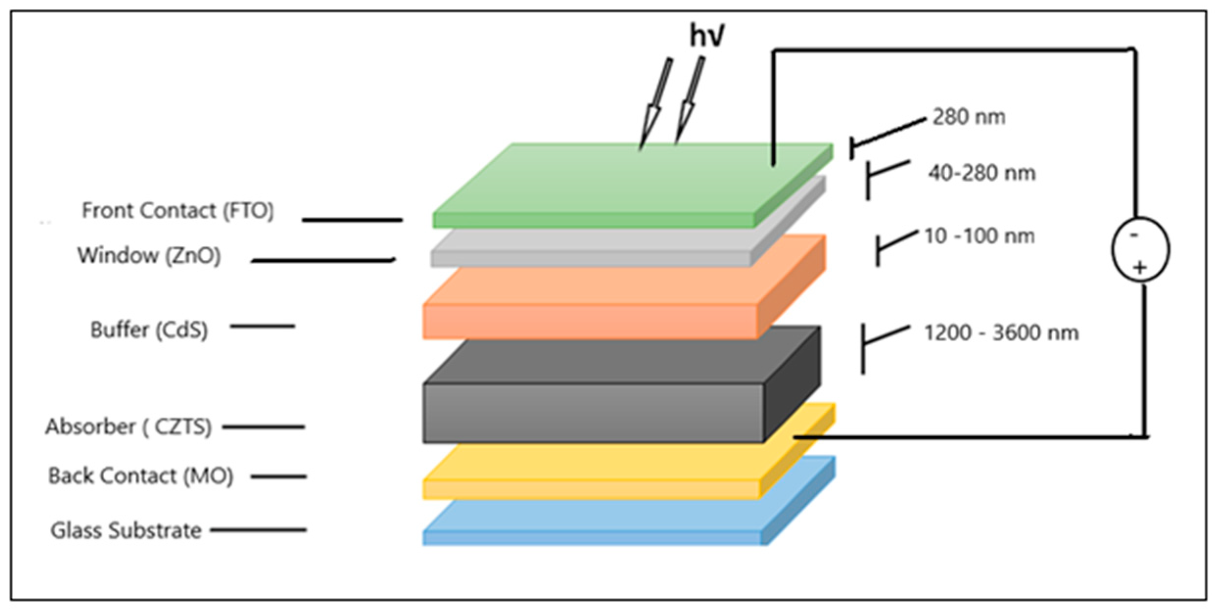
2.2. The Thin Film Solar Cell Device

The thin film solar cell device was constructed using a glass substrate as a back-supporting slide, a thin layer film of molybdenum (Mo) was deposited on the glass substrate layer, and a CZTST (p-type) layer with a thickness of (1200–3600 nm) was deposited on the molybdenum that was coated the back of the substrate glass. The CdS (n-type) used as a buffer layer with a thickness of (10–100 nm), ZnO layer (n-type) with a thickness of (40–280 nm) was used as a window, and FTO with a thickness (280 nm) was used as transparent conducting oxides (TCO). The materials for the modeling device were chosen for their efficiency, stability, low cost, and ease of preparation. The illustration for the modeling layers layout is shown in Figure 1. These essential components of a device are utilized to determine a solar cell’s electrical and photoelectric properties.

2.3. Material Parameters

Input parameters, also called physical parameters, are necessary to solve the fundamental semiconductor equations. In Table 1, physical characteristics such as layer thickness, electron-hole mobility, intrinsic carrier concentration, electron affinity, band gap, and doping density of absorber, buffer, and window layers are listed, as well as other physical characteristics used in SCAPS 1D software for numerical analysis. All simulations use 1.5AM solar radiation and a lighting source with a power density of 100 mW/cm2. Table 2 lists the functional properties of solar cells. The qualities of the back and front contact parameters are provided in Table 3. The device’s construction has two goals in common. The first includes evaluating and confirming real-world device behavior, while the second is simulating a device for certain physical parameters and predicting the outcomes. The behavior of the reference device (s) was accurately simulated, which is what device modeling is all about. To construct device modeling, physical or input parameters are acquired from referenced device experimental data. Predefined physical parameters such as carrier concentration densities and layer thickness are monitored and assessed using batch simulations. The SCAPS-1D software generates the   J - V characteristics curve, band alignment diagram, spectral response, and other functional parameters such as V O C , J S C , F F , and η , all of which are extremely important in the fabrication of an optimal photovoltaic cell device. All measurements are taken in both bright and dark conditions, and with regard to temperature. Temperature-dependent characteristics include thermal velocity and the effective density of states, whereas temperature-independent factors include band gap and mobility.

3. Results and Discussion

3.1. Effect of Layers Thickness on the Device Performance

3.1.1. Effect of CZTS Absorber (Acceptor) Layer Thickness on the Device Performance

The major objective of this section is to create a thinner CdTe layer without sacrificing device performance. As a result, the cost of manufacturing solar cells may be reduced by reducing the amount of materials used in the process. The absorber layer thickness of a device has a direct influence on conversion efficiency ( η ). The impact of the absorber layer (CZTS) thickness on solar cell performance is shown in Table 4 and Figure 2a. The influence of changing the thickness of the CZTS absorber layer from 1200 to 3600 nm on other material characteristics of different layers was investigated. When an absorber layer’s thickness is raised, J S C rises in tandem with the increase in V O C . The conversion efficiency rises up to a steady-state thickness of 2400 nm, whereas FF declines to a point where the ideal thickness is obtained. The conversion efficiency ( η ) will remain constant once the ideal settings are reached. Furthermore, increasing the thickness reduces the F F . The rise in J S C with increased V O C , is mostly due to increased absorption of longer wavelength photons, which affects the ration of photogenerated carriers. The absorber layer that was picked as the best has a thickness of 2400 nm. The thickness of the absorber layer, however, is one of the primary challenges with today’s large-scale and mass-production CZTS solar cells. The current focus of thin film solar cell research is on lowering the cost of thin film module production. Minimizing material usage by lowering film thickness is one approach to saving money. The photocurrent drops dramatically as the thickness of the photoactive layer is reduced, while the series resistance rises. Calculating the photocurrent density while considering the spectrum distribution of solar radiation can yield qualitative features of solar cell efficiency for varied photoactive layer thicknesses [30]. The wavelengths of light impact the emission of electron-hole pairs. These variations are caused by the thickness of the CZTS layer, as a thicker CZTS layer can absorb more photons across a broader wavelength range. The impact of CZTS thickness on Q E % is seen in Figure 2b, the Q E % was calculated for CdTe thicknesses ranging from 1200 to 3600 nm. When the CZTS layer thickness was increased, the Q E % increased. The layer thickness of more than 2400 nm has a little significant effect on the pace of Q E % increases. Q E % increases rapidly with CZTS layer thickness up to 2400 nm, then essentially saturates for thicknesses > 2400 nm due to incoming light absorption saturation. The Q E spectrum grows somewhat with CZTS layer thickness up to 3600 nm, since cell current increases dramatically after a CZTS layer of 2400 nm. As a consequence, the cell efficiency was optimized to 23.02%, corresponding to a CZTS layer thickness of 2400 nm. When demonstrated in Table 4, conversion efficiency rises by 3% as thickness rises from 1200 to 2400 nm, but only by 0.6% as thickness rises from 2400 to 3600 nm [31]. This indicates that a 2400 nm thickness is sufficient to absorb the vast majority of incoming photons. The number of produced electron-hole pairs will be reduced in thinner CZTS layer cells because the generation zone is near the high recombination back contact region, decreasing the quantum efficiency. In thicker CZTS layer cells, the production process occurs further away from the back. Finally, modeling results show that the ideal CZTS absorber layer thickness is 2400 nm, with a percent of 23.02%.

3.1.2. Effect of CdS Buffer (Donor) Layer Thickness on the Device Performance

The effect of buffer layer thickness on the performance of solar cells is also being explored. One of the main aims of this simulation is to reduce the optical and electrical losses in incoming radiation caused by the buffer layer. The buffer (CdS) layer thickness was increased from 10 to 100 nm. Simulated outcomes are shown in Table 5 and Figure 3a.
Table 5 demonstrates that increasing the buffer layer thickness has little impact on V O C , J S C , F F , and η %. As a result, it was determined that increasing the buffer layer thickness had no influence on the output of a solar device. The findings showed that as the thickness of the CdS layer grows, so does the cell performance. The thickness of CdS has a bigger influence on Jsc and η % values than F F and V O C . The non-significant impact on F F and V O C is due to photon losses that occur in a thicker CdS layer. As seen in Figure 3b, the bigger CdS buffer layer absorbs more photons from input radiation, reducing the number of photons reaching the absorption (CZTS) layer and lowering the Q E %. As a result, the quantity of electron-hole pairs created decreases. The Jsc and η % values were found to be substantially lower in thicker CdS films. Because the depletion layer thickness is lowered in the narrower CdS layer, the thinner CdS layer has a higher performance efficiency. The depletion layer appears to compensate for the lattice mismatch between the CdS and CZTS layers, which causes misfit dislocation. The thinner buffer layer causes a leakage current, whereas the thinner one causes a poor carrier separation rate. Layer thicknesses of less than 25 nm are not achievable because of restrictions in manufacturing techniques and equipment. As a consequence, the ideal and suggested buffer layer thickness is 25 nm. Photon absorption and quantum efficiency Q E % are affected by the thickness of the buffer layers (CdS). The intensity of the shortwave band falls when the thickness of the CdS buffer layer is increased. This indicates that the thin buffer layer has a large band response. The buffer leakage current falls as the CdS layer thickness decreases, increasing the breakdown voltage [32].

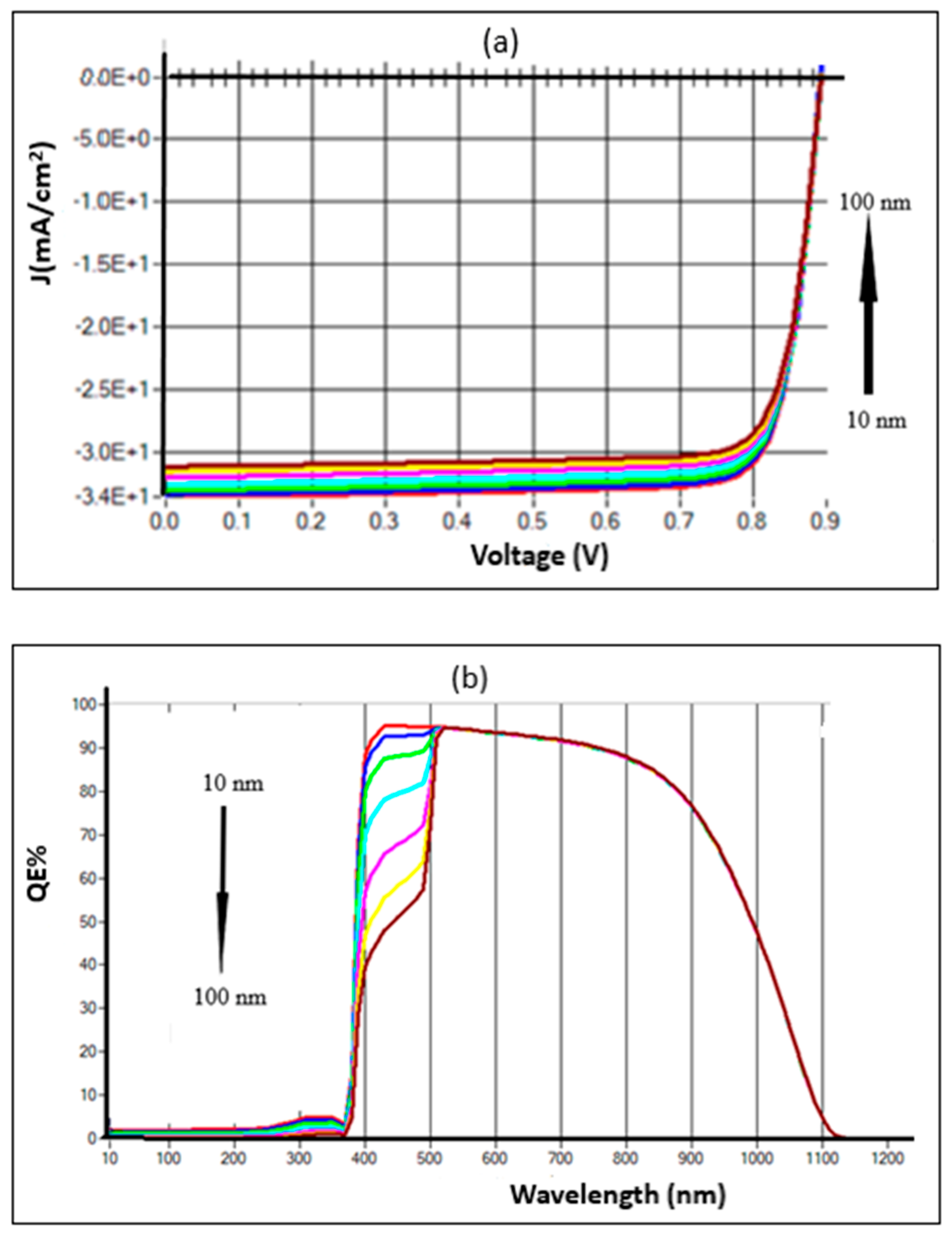
3.1.3. Effect of ZnO Window Layer Thickness on the Device Performance

Radiation from the incident source should flow through the ZnO (window) layer. ZnO has a bandgap of 3.3 eV and absorbs photons of λ < 300 nm in the UVC region. CZTS may absorb visible and infrared rays, which are completely transmitted through the ZnO layer [33]. Table 6 reveals that increasing the thickness of the ZnO layer has no influence on device performance ( V O C , J S C , F F , and η %). The link between device performance efficiency parameters and ZnO layer thickness is depicted in Figure 4a. Leakage current may occur if a very thin layer of ZnO is used, whereas a layer that is too thick may result in poor carrier separation rate. Finally, 120 nm is chosen as the optimum and recommended layer. As demonstrated in Figure 4b, the Q E % is unaffected by changes in buffer thickness in the range (40 nm to 280 nm). This may be ascribed to the window layer sharing a little amount of electron-hole pair creation. Finally, the 120 nm layer is chosen as the optimal and preferable layer.

3.2. Effect of Doping Concentration on the Device Performance

3.2.1. Effect of CZTS Absorber (Acceptor) Doping Concentration on the Device Performance

Figure 5a and Table 7 exhibit the acceptor doping concentration simulation findings. The concentration of the acceptor was adjusted from 1 × 1016 cm−3 to 1 × 1017 cm−3. Table 7 shows that when the doping concentration increases, J S C falls while V O C increases. The fundamental reason for this is that when the acceptor carrier concentration rises, so does the device’s saturation current, and as a result, V O C rises. J S C diminishes as carrier densities rise, accelerating the recombination process and reducing the likelihood of collecting photon-generated electrons.
This is due to an increase in the recombination of free carrier charges within the bulk. Longer wavelength, lower energy photons are completely absorbed in the CZTS layer. As a result, the influence of the concentration density on the collected conversion efficiency is greater. can be seen in Table 7, as the carrier concentration in the absorber layer material rises, F F and η% rise as well. η and FF stay constant until achieving the optimum acceptor carrier concentration, but V O C steadily rises. The higher efficiency in the simulated findings is explained by the combined impact of current density J S C saturation, as well as the quick increase in V O C and FF with acceptor carrier charge concentration (NA). As a result, the best CdTe thin film performance can be attained with ( N A ~5.5 × 1016 cm−3). The following Equation (12) explains the PN junction model [34]:
I O = A q n i 2 ( D e L e N A   + D h L h N D )
I O stands for saturation current, n i for intrinsic concentration, A   for diode quality factor, q   for elementary charge, T for temperature,   k for Boltzmann constant, I L for light-generated current, L   and D for diffusion length and coefficient, and N D and N A for donor and acceptor charge concentrations, respectively. The letters h and e stand for holes and electrons, respectively. As the acceptor carrier concentration N A rises, the saturation current I O falls, resulting in an increase in V O C and a drop in J S C .
When the acceptor carrier concentration is high, the recombination process speeds up and lowers the possibility of electron-hole pair production, reducing the Q E % of long wavelength photons. The absorber (CZTS) layer will absorb long-wavelength light very efficiently. The effect of modifications in CZTS acceptor charge carrier concentration ( N A ) on solar cell fundamental characteristics was thoroughly examined. The spectrum response of the thin film with CdTe acceptor carrier charge concentration is shown in Figure 5b ( N A ). The simulated findings show that when the acceptor concentration increases from 1 × 1016 cm−3 to 1 × 1017 cm−3, the external quantum efficiency ( Q E ) decreases. The greater gathering of photons at longer wavelengths can be ascribed to this. The thin film solar cell has created more electron-hole pairs as a result of the absorption of longer wavelength photons, resulting in an increase in Jsc at low acceptor charge carrier concentration ( N A ) (Table 7). The J-V curves show that as the acceptor charge carrier concentration ( N A ) of the CdTe layer is increased ( N A > 1 × 10 16   cm 3 ), V O C rises. This rise implies that the open-circuit voltage ( V O C ) of the CdTe layer is highly influenced by the acceptor charge carrier concentration ( N A ). The generated electric field in the depletion area is influenced when the acceptor (hole) carrier charge concentration of ( N A ) of the CdTe layer is high. As a result, the free charge carrier recombination decreases, increasing the V O C . While lowering the CdTe acceptor carrier charge concentration below 1 × 10 16   cm 3 , causes higher optical losses, which might be due to back contact surface recombination. The rear contact is made using a tiny layer of molybdenum (Mo). It has the ability to make ohmic contact with CZTS. Mo may react with sulfide (S) during CZTS deposition to form MoS2. As a result, the CZTS/Mo structure becomes the CZTS/MoS2/MO structure. The addition of MoS2 provides an ohmic behavior to the CZTS/Mo hetero-contact while reducing recombination at the interface. The MoS2 layer works as a barrier height for photo-generated carriers. The barrier causes high serial resistance (corrosion-resistant), which lowers the Voc, FF, and hence the conversion efficiency of the device [35,36].

3.2.2. Effect of CdS Buffer (Donor) Doping Concentration on the Device Performance

This section’s major goal is to minimize the buffer layer’s losses (both optical and electrical). The carrier charge concentration level of the CdS layer was altered from 1 × 10¹⁷ to 1 × 1018 cm−3 after that. Figure 6a and Table 8 illustrate the outcomes of the donor concentration simulation. J S C and V O C are nearly constant as doping concentration increases, as shown in Table 8. The device’s η % and FF have changed little as the doping concentration has increased. When we increase the doping concentration in a buffer layer beyond the ideal level (2.5 × 1017 cm−3), the device’s η % and FF remain constant and begin to decline. As a result, the buffer layer’s final ideal concentration value was 2.5 × 1017 cm−3. According to Figure 6a, increasing the doping concentration in the buffer layer has no significant effect on the device’s operation. As a consequence, it was deduced that a change in buffer layer concentration had no effect on the total output of a photovoltaic device. More incoming photons created by the CdS layer are absorbed when the buffer layer ( N D ) concentration falls, lowering the number of photons that the absorber (CZTS) layer can absorb. As demonstrated in Figure 6b, absorbed photons form fewer electron-hole pairs, resulting in a lower Q E % . It can be seen that the Q E % increases as the donor carrier charge concentrations rise. Based on the above, it is recommended to have a high buffer layer donner concentration ( N D 2.5 × 10 17   cm 3 ) in the simulation for thin films.

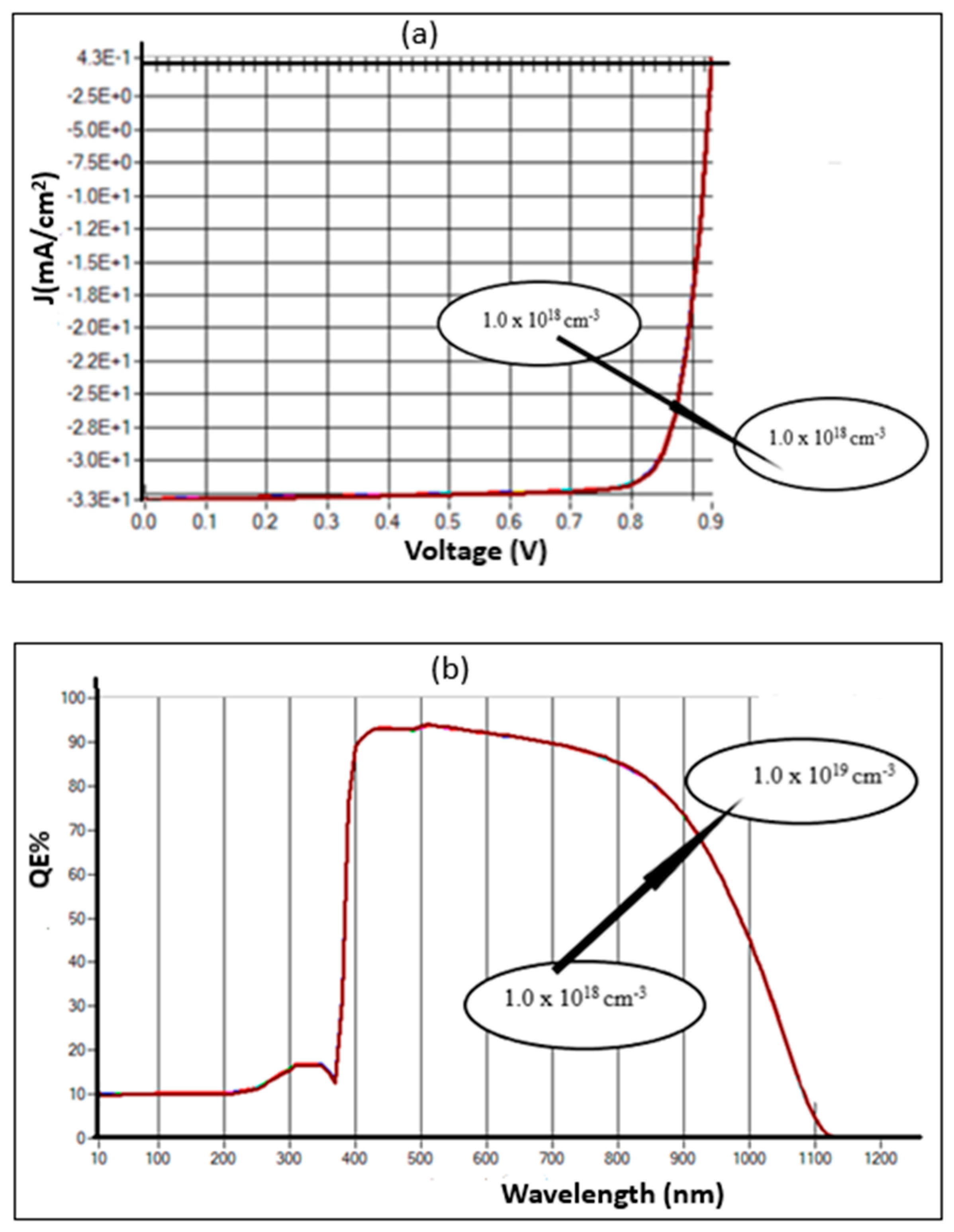
3.2.3. Effect of ZnO Window Doping Concentration on the Device Performance

Both optical and electrical access is provided by ZnO (window) layers. Because of its optical bandgap of 3.3 eV, ZnO was chosen as the window in our scenario because it covers the whole visible wavelength. It can be deduced from Figure 7a,b, as well as Table 9, that the efficiency parameters and Q E % percent are unaffected by changes in donor doping concentration in the range of (1.0 × 1018 cm−3 to 1.0 × 1019 cm−3), that the window layer contributes a small amount to electron-hole pair generation. The ZnO donor carrier concentration was measured ( N D     4 × 1018 cm−3). The window layer (ZnO) has a greater bandgap and n-type conductivity than the absorber layer. It has an electrical function in that it adjusts the width of the prohibited band between the absorber and the window layer, preventing carrier recombination at the interface. It also has an optical function in that, due to its large bandgap, it can absorb the maximum of the light spectrum in the area not absorbed by the active layer, minimizing optical losses, and a mechanical function in that it adjusts the width of the prohibited band between the absorber and the window layer, preventing carrier recombination. The purpose of a protective layer is to shield the absorber’s surface during the deposition of the ZnO layer, which might result in faults on the CZTS surface. Because the ZnO layer is so thin in comparison to the CZTS absorber layer, carrier density in the ZnO area has little effect on cell performance [31,37,38].

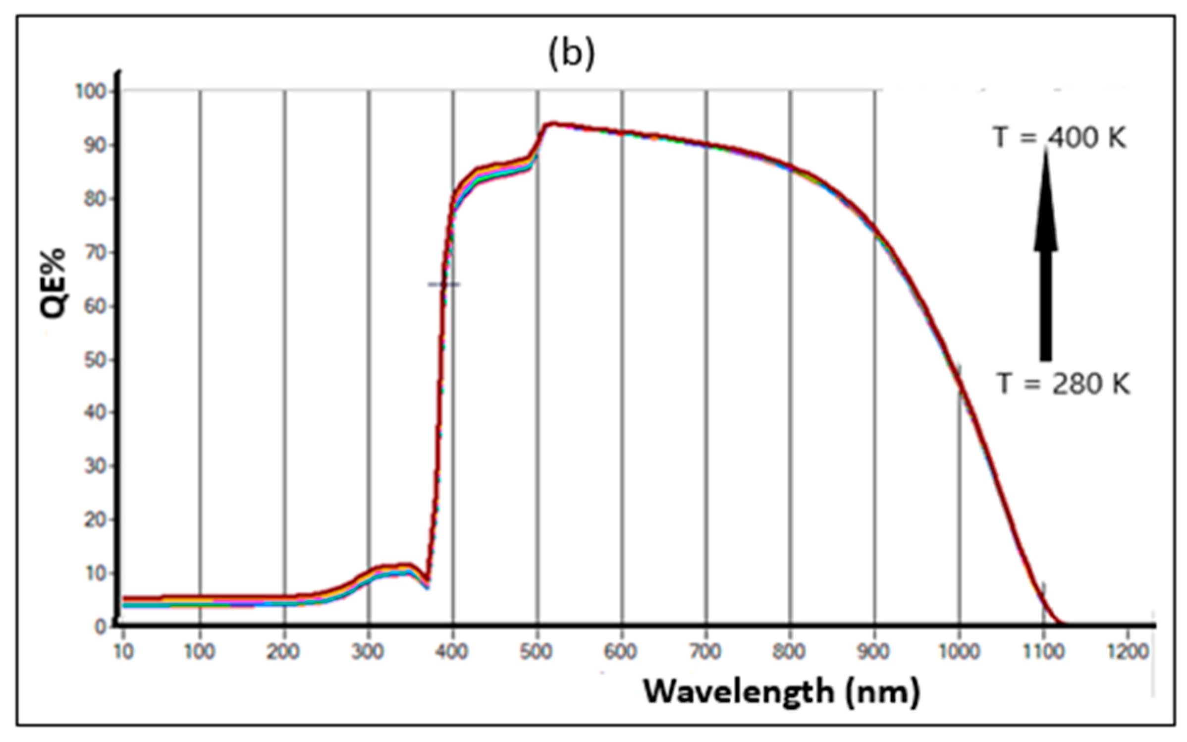
3.3. Effect of Working Temperature on the Device Performance

The operating temperature has a significant impact on photovoltaic device performance in thin film solar cell applications. The photovoltaic panels are exposed to the elements. As a result of incident light, heating on solar cells increases, affecting photovoltaic cell performance. At temperatures exceeding 300 K, the solar cell panels are operational. The influence of the operating temperature of the suggested cell is also investigated. For research purposes, the temperature was measured in the range of 280 to 400 K. The simulation results are depicted in Figure 8a. The V O C of a solar cell is directly affected by temperature, which has an impact on the overall performance of the cell. The performance of photovoltaic cells declines as the temperature rises. The increased temperature affects the material carrier concentration, band gaps, and electron and hole mobility, resulting in a lower cell conversion efficiency η% [39]. The reverse saturation current, J o , is temperature dependent because V O C decreases as temperature rises. As stated in Equation (13), the reverse saturation current increases as the temperature rises, and this increase in current is the principal cause of the decline in V O C [40].
J e = J o ( e q V O C k B T 1 )
where J e is the photocurrent created by light. The higher the operational temperature, the more energy electrons have. Because of the higher temperature, these electrons are more likely to recombine with holes before reaching the depletion area. The solar cell efficiency characteristics are shown in Table 10 which shows that when the temperature rises, the device’s conversion efficiency decreases. According to Equation (12), a rise in operating temperature affects F F and V O C , whereas J S C climbs marginally to a stable limit with an increase in operating temperature (no significant effect). This is owing to the temperate-affected drop in band-gap energy [41]. As a result, more far-reaching radiation photons are able to form electron-hole pairs. V O C , on the other hand, decreases significantly when the temperature rises. The reverse saturation current ( I S ), which is temperature sensitive, is responsible for the reduction in V O C levels with increasing temperature [42]. The inherent carrier concentration [43] is another important component that causes the decrease in V O C with increasing operating temperature. The absorber layer’s bandgap is usually rather small. The electron-hole pair recombination may be aided by the narrower bandgaps. The interatomic spacing rises as the amplitude of the atomic vibrations increases owing to increased thermal energy [44]. This behavior may be better understood if one thinks that the interatomic spacing grows when the amplitude of the atomic vibrations increases. The linear expansion coefficient of a material is used to quantify this impact. The potential observed by electrons in the material decreases as interatomic separation increases, reducing the energy bandgap. With increasing temperature, the FF percent decreases until it reaches a steady-state temperature limit. Finally, when the temperature rises, the device’s conversion efficiency decreases.
Quantum efficiency percent (QE%) profiles at different temperature values are shown in Figure 8b. The QE% profiles were calculated based on the SCAPS-1D software program. The QE% profiles show a peak response to illumination wavelength. The QE% ranged (80–90%) in the wavelength range (520–800 nm) and started lowering to 45% in the range below (300–520 nm). Recombination and absorption in the absorber and buffer layer cause the decrease. A rise in temperature in the range of 2800–400 K had a minor effect on the quantum efficiency. The QE% profile shows absorption maxima at ≈530 nm, this value is consistent with the input CZTS value ( E g = 1.45 eV). Figure 8b shows an absorption edge at 800 nm, which can be attributed to vacancy levels in the energy gap, which can be produced by doping. In addition, a minor effect in quantum efficiency with temperature was observed, which can be attributed to the short period in the studied temperature range (280–400 K), which meant that the range could not cause a noticeable effect on the semiconductor construction, and thus only a minor change in quantum efficiency was observed [45,46].

3.4. Optimization of the FTO/ZnO/CdS/CZTS/MO Thin Film-Based Solar Cell

3.4.1. J - V Characteristics at Optimum

The primary function of a photovoltaic cell is to convert light energy into electrical energy. In the dark, when there is no light, the photovoltaic solar cell is a massive flat diode that forms the exponential J-V curve. Due to minority carriers, the cell gives an exceptionally low current value in dark environments. The solar cell begins to work when exposed to light, and current flows due to charge carriers produced by incident photons. The cross-over and roll-over of the J - V curves of the FTO/ZnO/CdS/CZTS/MO thin film: The intersection of dark and lit J-V curves is known as cross-over. The phenomenon of roll-over occurs when the J - V curve is meshed and current levels of greater voltage are present. The dark and photo J - V curves are depicted in Figure 9. The simulation of SCAPS-1D depends the optimal layer carrier concentration densities in its calculation CZTS (W = 2400 nm, N A = 5.5 × 1016 cm−3), CdS (W = 25 nm, N D = 2.5 × 1017 cm−3), and ZnO (W = 120 nm, N D = 4 × 1018 cm−3). The optimum output cell efficiency parameters were achieved with the conversion efficiency ( η %) of 25.72% (FF% ≈ 83.75%, J S C   ≈ 32.96436 mA/cm2, and V O C ≈ 0.9315 V). The carrier concentration of the absorber layer/buffer layer interface recombination or the absorber/back contact was measured using this advantage [47].

3.4.2. Energy Band Gap at Optimum

The energy band diagram of FTO/ZnO/CdS/CZTS/MO solar cells is shown in Figure 10a,b. This energy band diagram was generated from the SCAPS output for this study. The energy band diagram is useful for understanding solar cell properties. More or equal to 1.45 eV, is the band gap value for incident light photons that is optimum for most of the light to be absorbed for effective conversion efficiency. Band alignment is one of the most important factors influencing thin film performance and current transmission across the heterojunction. CZTS as the absorber layer has an excellent band diagram, with CdS as the buffer layer and ZnO as the window layer. Figure 10a shows the CZTS absorber layer ( E g = 1.45 eV) from 0 to 2.4 μm, the CdS buffer layer ( E g = 2.4 eV), the ZnO window layer ( E g = 3.3 eV) from 2.425 to 2.545 μm, and the FTO layer ( E g = 3.5 eV) from 2.545 to 2.825 μm. A “cliff” type band alignment occurs when the absorber layer’s conduction band is higher than the buffer layer’s conduction band [48]. This is the case of CZTS as a thin film absorber, as seen in Figure 10b. The absorber, buffer, and window layers may all be seen to have adequate band alignment. The band diagram depicts four recombination zones. The four locations include recombination at the back contact (region R1), bulk (quasi-neutral) recombination in the absorber layer (region R2), space charge (region R3), and recombination at the absorber/buffer interface (region R4). The back-contact will be kept near to the depletion zone by the thin absorber layer, resulting in a significant increase in back-contact recombination. Reasonable neutral interface flaws for recombination at the CZTS/CdS and CdS/ZnO interfaces were also investigated at mid-gap to facilitate recombination [28]. The rear and front contact surfaces’ reflectance’s were set to 0.1 and 0.9, respectively (Table 3). When photons transit the absorber, they are reflected by the absorber’s high reflectivity upon return contact, which boosts absorption.

3.5. Comparison the Simulation Results with Experimental Thin Film-Based Solar Cell

Table 11 show the results of our suggested modeling work for thin film FTO/ZnO/CdS/CZTS/MO compared to earlier experimental work.

4. Conclusions

The SCAPS program was used to model and analyze a kesterite FTO/ZnO/CdS/CZTS/MO -based solar cell. Researchers, designers, and engineers will find this work extremely valuable in studying and constructing CZTS-based systems. It should be emphasized that using J - V characteristics to explain the device’s behavior is insufficient to fully comprehend the solar cell, which is due to the fact that the solar cell’s reaction is also influenced by its internal physical mechanism. Several variables, as well as various alternative simulation situations, must be addressed to improve the confidence in the modeling of a solar cell. This work achieved encouraging optimized results with a conversion efficiency ( η %) of 25.72% ( F F % ≈ 83.75%, J S C   ≈ 32.96436 mA/cm2 and V O C ≈ 0.9315 V). The findings will provide crucial information for the production of high-efficiency thin film solar cells. The development of enhanced numerical modeling performance of solar cells plays a vital role, as evidenced by the findings.

Author Contributions

Data curation, S.H.Z.; Formal analysis, S.H.Z. and A.H.Z.; Investigation, S.H.Z., N.M.A. and A.R.P.; Methodology, S.H.Z. and A.H.Z.; Project administration, S.H.Z.; Resources, S.H.Z. and A.H.Z.; Software, S.H.Z. and N.M.A.; Validation, S.H.Z., S.N.K. and A.H.Z.; Visualization, S.H.Z.; Writing—original draft, S.H.Z., A.H.Z. and A.R.P.; Writing—review & editing, S.H.Z., A.H.Z., N.M.A., A.R.P., M.S. and A.F.I.A. All authors have read and agreed to the published version of the manuscript.

Funding

This research received no external funding.

Institutional Review Board Statement

Not applicable.

Informed Consent Statement

Not applicable.

Acknowledgments

The authors would like to acknowledge the University of Gent, Belgium, for providing the SCAPS simulator. Also, they authors would like to acknowledge the MOU between Universiti Sains Malaysia and Ajman University U2021085 for the research collaboration. Furthermore, we are grateful to Ajman University for supporting this study.

Conflicts of Interest

The authors declare that there are no conflicts of interest in this work.

References

  1. Mariotti, N.; Bonomo, M.; Fagiolari, L.; Barbero, N.; Gerbaldi, C.; Bella, F.; Barolo, C. Recent advances in eco-friendly and cost-effective materials towards sustainable dye-sensitized solar cells. Green Chem. 2020, 22, 7168–7218. [Google Scholar] [CrossRef]
  2. Jacoby, M. The future of low-cost solar cells. Chem. Eng. News 2016, 94, 30–35. [Google Scholar]
  3. Sciuto, G.L.; Salvatore, C. A 3D finite element model of degradation phenomena in organic solar devices affected by oxidation. Int. J. Energy Environ. Eng. 2020, 11, 431–437. [Google Scholar] [CrossRef]
  4. Banu, S.; Ahn, S.J.; Ahn, S.K.; Yoon, K.; Cho, A. Fabrication and characterization of cost-efficient CuSbS2 thin film solar cells using hybrid inks. Sol. Energy Mater. Sol. Cells 2016, 151, 14–23. [Google Scholar] [CrossRef]
  5. Repins, I.L.; Romero, M.J.; Li, J.V.; Wei, S.-H.; Kuciauskas, D.; Jiang, C.-S.; Beall, C.; Dehart, C.; Mann, J.; Hsu, W.-C.; et al. Kesterite Successes, Ongoing Work, and Challenges: A Perspective From Vacuum Deposition. IEEE J. Photovolt. 2012, 3, 439–445. [Google Scholar] [CrossRef]
  6. Yadav, M.C.; Krishnan, S.; Mohammad, F.; Al-Lohedan, H.A. Fabrication and application of graphene-based composites for indoor air quality and wastewater treatment. In Graphene-Based Nanotechnologies for Energy and Environment; Elsevier BV: Amsterdam, The Netherlands, 2019; pp. 359–387. [Google Scholar]
  7. Zhou, H.; Hsu, W.C.; Duan, H.S.; Bob, B.; Yang, W.; Song, T.B.; Hsu, C.-J.; Yang, Y. CZTS nanocrystals: A promising approach for next generation thin film photovoltaics. Energy Environ. Sci. 2013, 6, 2822–2838. [Google Scholar] [CrossRef]
  8. Xinkun, W.; Wei, L.; Shuying, C.; Yunfeng, L.; Hongjie, J. Photoelectric properties of Cu2ZnSnS4 thin films deposited by thermal evaporation. J. Semicond. 2012, 33, 022002. [Google Scholar]
  9. International Electrotechnical Commission 2016 Terrestrial Photovoltaic (PV) Modules—Design Qualification and Type Approval—Part 1-4: Special Requirements for Testing of Thin-Film Cu (In,Ga) (S,Se) 2 Based Photovoltaic (PV) Modules; IEC Standard No. 61215-1-4; Canadian Standards Association: Toronto, ON, Canada, 2021.
  10. International Electrotechnical Commission 2016 Terrestrial Photovoltaic (PV) Modules—Design Qualification and Type Approval—Part 2: Test Procedures; IEC Standard No. 61215-2; American National Standards Institute: New York, NY, USA, 2016.
  11. Khattak, Y.H.; Baig, F.; Ullah, S.; Marí, B.; Beg, S.; Ullah, H. Enhancement of the conversion efficiency of thin film kesterite solar cell. J. Renew. Sustain. Energy 2018, 10, 033501. [Google Scholar] [CrossRef]
  12. Hussain, S.; Rehman, Z.U.; Mohammad, N.; Tahir, M.; Shahzada, K.; Khan, S.W.; Salman, M.; Khan, M.; Gul, A. Numerical Modeling for Engineering Analysis and Designing of Optimum Support Systems for Headrace Tunnel. Adv. Civ. Eng. 2018, 2018, 7159873. [Google Scholar] [CrossRef]
  13. Haddout, A.; Raidou, A.; Fahoume, M. A review on the numerical modeling of CdS/CZTS-based solar cells. Appl. Phys. A 2019, 125, 124. [Google Scholar] [CrossRef]
  14. Theraja, B.L. A Textbook of Electrical Technology; S. Chand Publishing: New Delhi, India, 2008. [Google Scholar]
  15. Naidu, S.M. A Text Book of Applied Physics; Pearson Education: New Delhi, India, 2009. [Google Scholar]
  16. Li, S.S. Photonic Devices. In Semiconductor Physical Electronics; Springer: Boston, MA, USA, 1993; pp. 327–390. [Google Scholar]
  17. Amin, N.; Yamada, A.; Konagai, M. Effect of ZnTe and CdZnTe Alloys at the Back Contact of 1-µm-Thick CdTe Thin Film Solar Cells. Jpn. J. Appl. Phys. 2002, 41, 2834–2841. [Google Scholar] [CrossRef]
  18. Ullah, H.; Marí, B.; Cui, H.N. Investigation on the Effect of Gallium on the Efficiency of CIGS Solar Cells through Dedicated Software. Appl. Mech. Mater. 2013, 448–453, 1497–1501. [Google Scholar] [CrossRef]
  19. Paudel, N.; Wieland, K.; Compaan, A. Ultrathin CdS/CdTe solar cells by sputtering. Sol. Energy Mater. Sol. Cells 2012, 105, 109–112. [Google Scholar] [CrossRef]
  20. Singh, P.; Ravindra, N. Temperature dependence of solar cell performance—An analysis. Sol. Energy Mater. Sol. Cells 2012, 101, 36–45. [Google Scholar] [CrossRef]
  21. Hegedus, S.S.; Shafarman, W.N. Thin-film solar cells: Device measurements and analysis. Prog. Photovolt. Res. Appl. 2004, 12, 155–176. [Google Scholar] [CrossRef]
  22. Simya, O.; Mahaboobbatcha, A.; Balachander, K. A comparative study on the performance of Kesterite based thin film solar cells using SCAPS simulation program. Superlattices Microstruct. 2015, 82, 248–261. [Google Scholar] [CrossRef]
  23. Niemegeers, A.; Burgelman, M. Numerical modelling of ac-characteristics of CdTe and CIS solar cells. In Proceedings of the Conference Record of the Twenty Fifth IEEE Photovoltaic Specialists Conference-1996, Washington, DC, USA, 13–17 May 1996; pp. 901–904. [Google Scholar]
  24. Decock, K.; Zabierowski, P.; Burgelman, M. Modeling metastabilities in chalcopyrite-based thin film solar cells. J. Appl. Phys. 2012, 111, 43703. [Google Scholar] [CrossRef] [Green Version]
  25. Burgelman, M.; Verschraegen, J.; Degrave, S.; Nollet, P. Modeling thin-film PV devices. Prog. Photovolt. Res. Appl. 2004, 12, 143–153. [Google Scholar] [CrossRef]
  26. Movla, H. Optimization of the CIGS based thin film solar cells: Numerical simulation and analysis. Optik 2014, 125, 67–70. [Google Scholar] [CrossRef]
  27. Shin, B.; Gunawan, O.; Zhu, Y.; Bojarczuk, N.A.; Chey, S.J.; Guha, S. Thin film solar cell with 8.4% power conversion efficiency using an earth-abundant Cu2ZnSnS4 absorber. Prog. Photovolt. Res. Appl. 2013, 21, 72–76. [Google Scholar] [CrossRef]
  28. Zhao, W.; Zhou, W.; Miao, X. Numerical simulation of CZTS thin film solar cell. In Proceedings of the 2012 7th IEEE International Conference on Nano/Micro Engineered and Molecular Systems (NEMS), Kyoto, Japan, 5–8 March 2012; IEEE: Piscataway, NJ, USA, 2012; pp. 502–505. [Google Scholar]
  29. Adewoyin, A.D.; Olopade, M.A.; Chendo, M. Enhancement of the conversion efficiency of Cu2ZnSnS4 thin film solar cell through the optimization of some device parameters. Optik 2017, 133, 122–131. [Google Scholar] [CrossRef]
  30. Urbina, A. The balance between efficiency, stability and environmental impacts in perovskite solar cells: A review. J. Phys. Energy 2019, 2, 022001. [Google Scholar] [CrossRef]
  31. Kuddus, A.; Mostaque, S.K.; Hossain, J. Simulating the performance of a high-efficiency SnS-based dual-heterojunction thin film solar cell. Opt. Mater. Express 2021, 11, 3812. [Google Scholar] [CrossRef]
  32. Hinoki, A.; Kamiya, S.; Tsuchiya, T.; Yamada, T.; Kikawa, J.; Araki, T.; Suzuki, A.; Nanishi, Y. Correlation between the leakage current and the thickness of GaN-layer of AlGaN/GaN-HFET. Phys. Status Solidi C 2007, 4, 2728–2731. [Google Scholar] [CrossRef]
  33. Kaur, N.; Singh, M.; Pathak, D.; Wagner, T.; Nunzi, J.-M. Organic materials for photovoltaic applications: Review and mechanism. Synth. Met. 2014, 190, 20–26. [Google Scholar] [CrossRef]
  34. Luque, A.; Hegedus, S. Photovoltaic Science and Engineering; John Wiley & Sons Ltd.: Chichester, UK, 2003. [Google Scholar]
  35. Mak, K.F.; Lee, C.; Hone, J.; Shan, J.; Heinz, T.F. Atomically thin MoS 2: A new direct-gap semiconductor. Phys. Rev. Lett. 2010, 105, 136805. [Google Scholar] [CrossRef] [Green Version]
  36. Zyoud, S.H.; Zyoud, A.H. Effect of Absorber (Acceptor) and Buffer (Donor) Layers Thickness on Mo/CdTe/CdS/ITO Thin Film Solar Cell Performance: SCAPS–1D Simulation Aspect. Int. Rev. Model. Simul. 2021, 14, 10–17. [Google Scholar] [CrossRef]
  37. Kara, R.; Rachid, S.; Azizi, A. Effect of i-ZnO seed layer on the properties of electrodeposited p-Cu2O/n-ZnO/FTO heterojunction thin films. Mater. Res. Express 2019, 6, 126402. [Google Scholar] [CrossRef]
  38. Tobbeche, S.; Kalache, S.; Elbar, M.; Kateb, M.N.; Serdouk, M.R. Improvement of the CIGS solar cell performance: Structure based on a ZnS buffer layer. Opt. Quantum Electron. 2019, 51, 1–13. [Google Scholar] [CrossRef]
  39. Hossain, S.; Amin, N.; Martin, M.A.; Aliyu, M.M.; Razykov, T.; Sopian, K. A numerical study on the prospects of high efficiency ultra thin ZnxCd1−xS/CdTe Solar Cell. Chalcogenide Lett. 2011, 8, 263–272. [Google Scholar]
  40. Sha, W.E.; Ren, X.; Chen, L.; Choy, W.C. The efficiency limit of CH3NH3PbI3 perovskite solar cells. Appl. Phys. Lett. 2015, 106, 221104. [Google Scholar] [CrossRef] [Green Version]
  41. Zyoud, S.H.; Abdelkader, A.; Zyoud, A.H. The Impact of Temperature on the Performance of Semiconductor Laser Diode. Int. J. Adv. Sci. Technol. 2020, 29, 1167–1180. [Google Scholar]
  42. Al-Khazzar, A.A.A. Behavior of four Solar PV modules with temperature variation. Int. J. Renew. Energy Res. 2016, 6, 1091–1099. [Google Scholar]
  43. Sproul, A.B.; Green, M.A. Intrinsic carrier concentration and minority-carrier mobility of silicon from 77 to 300 K. J. Appl. Phys. 1993, 73, 1214–1225. [Google Scholar] [CrossRef]
  44. Gong, J.W.; Chen, Q.F.; Lian, M.R.; Liu, N.C.; Daoust, C. Temperature feedback control for improving the stability of a semiconductor-metal-oxide (SMO) gas sensor. IEEE Sens. J. 2006, 6, 139–145. [Google Scholar]
  45. Zyoud, S.H.; Zyoud, A.H.; Ahmed, N.M.; Abdelkader, A.F.I. Numerical Modelling Analysis for Carrier Concentration Level Optimization of CdTe Heterojunction Thin Film–Based Solar Cell with Different Non–Toxic Metal Chalcogenide Buffer Layers Replacements: Using SCAPS–1D Software. Crystals 2021, 11, 145. [Google Scholar]
  46. Xiao, B.; Zhu, M.; Zhang, B.; Dong, J.; Ji, L.; Yu, H.; Sun, X.; Jie, W.; Xu, Y. Optical and electrical properties of vanadium-doped ZnTe crystals grown by the temperature gradient solution method. Opt. Mater. Express 2018, 8, 431–439. [Google Scholar] [CrossRef]
  47. Niemegeers, A.; Burgelman, M. Effects of the Au/CdTe back contact on IV and CV characteristics of Au/CdTe/CdS/TCO solar cells. J. Appl. Phys. 1997, 81, 2881–2886. [Google Scholar] [CrossRef]
  48. Zyoud, S.H.; Zyoud, A.H.; Abdelkader, A.; Ahmed, N.M. Numerical Simulation for Optimization of ZnTe-Based Thin-Film Heterojunction Solar Cells with Different Metal Chalcogenide Buffer Layers Replacements: SCAPS–1D Simulation Program. Int. Rev. Model. Simul. 2021, 14, 79–88. [Google Scholar] [CrossRef]
  49. Tajima, S.; Umehara, M.; Hasegawa, M.; Mise, T.; Itoh, T. Cu2ZnSnS4 photovoltaic cell with improved efficiency fabricated by high-temperature annealing after CdS buffer-layer deposition. Prog. Photovolt. Res. Appl. 2016, 25, 14–22. [Google Scholar] [CrossRef] [Green Version]
  50. Patel, M.; Ray, A. Enhancement of output performance of Cu2ZnSnS4 thin film solar cells—A numerical simulation approach and comparison to experiments. Phys. B Condens. Matter 2012, 407, 4391–4397. [Google Scholar] [CrossRef]
  51. Ahmed, S.; Reuter, K.B.; Gunawan, O.; Guo, L.; Romankiw, L.T.; Deligianni, H. A High Efficiency Electrodeposited Cu2ZnSnS4 Solar Cell. Adv. Energy Mater. 2012, 2, 253–259. [Google Scholar] [CrossRef]
  52. Tao, J.; Liu, J.; Chen, L.; Cao, H.; Meng, X.; Zhang, Y.; Zhang, C.; Sun, L.; Yang, P.; Chu, J. 7.1% efficient co-electroplated Cu2ZnSnS4 thin film solar cells with sputtered CdS buffer layers. Green Chem. 2016, 18, 550–557. [Google Scholar] [CrossRef]
  53. Wang, K.; Gunawan, O.; Todorov, T.K.; Shin, B.; Chey, S.J.; Bojarczuk, N.A.; Mitzi, D.B.; Guha, S. Thermally evaporated Cu2ZnSnS4 solar cells. Appl. Phys. Lett. 2010, 97, 143508. [Google Scholar] [CrossRef]
  54. Katagiri, H.; Jimbo, K.; Maw, W.S.; Oishi, K.; Yamazaki, M.; Araki, H.; Takeuchi, A. Development of CZTS-based thin film solar cells. Thin Solid Film. 2009, 517, 2455–2460. [Google Scholar] [CrossRef]
  55. Chen, S.; Walsh, A.; Gong, X.-G.; Wei, S.-H. Classification of Lattice Defects in the Kesterite Cu2ZnSnS4 and Cu2ZnSnSe4 Earth-Abundant Solar Cell Absorbers. Adv. Mater. 2013, 25, 1522–1539. [Google Scholar] [CrossRef]
  56. Yin, L.; Cheng, G.; Feng, Y.; Li, Z.; Yang, C.; Xiao, X. Limitation factors for the performance of kesterite Cu2ZnSnS4 thin film solar cells studied by defect characterization. RSC Adv. 2015, 5, 40369–40374. [Google Scholar] [CrossRef]
Figure 1. Schematic diagram of thin film.
Crystals 11 01468 g001
Figure 2. (a)   J - V current curves, (b) quantum efficiency percentage ( Q E % ) for the cell at different thickness CZTS layer, CdS, ZnO, and FTO layer thicknesses are 100 nm, 200 nm, and 280 nm, respectively, T = 300 K.
Crystals 11 01468 g002
Figure 3. (a) J - V current curves, (b) quantum efficiency percentage ( Q E % ) for the cell at different thickness CdS layer, CZTS, ZnO, and FTO layer thicknesses are 2400 nm, 200 nm, and 280 nm, respectively, T = 300 K.
Crystals 11 01468 g003
Figure 4. (a) J - V current curves, (b) quantum efficiency percentage (QE%) for the cell at different thickness ZnS layer, CZTS, CdS, and FTO layer thicknesses are 2400 nm, 25 nm, and 280 nm, respectively, T = 300 K.
Crystals 11 01468 g004aCrystals 11 01468 g004b
Figure 5. (a) J - V current curves, (b) quantum efficiency percentage (QE%) for the cell as a function of CZTS acceptor carrier concentration ( N A ), T = 300.
Crystals 11 01468 g005
Figure 6. (a) J - V current curves, (b) quantum efficiency percentage (QE%) for the cell as a function of CdS donor carrier concentration ( N D ), T = 300 K.
Crystals 11 01468 g006
Figure 7. (a) J - V current curves, (b) quantum efficiency percentage ( Q E % ) for the cell as a function of ZnO donor carrier concentration ( N D ), T = 300 K.
Crystals 11 01468 g007
Figure 8. (a) J - V current curves, (b) quantum efficiency percentage (QE%) for the cell as a function of temperature.
Crystals 11 01468 g008aCrystals 11 01468 g008b
Figure 9. J - V current curves for optimum thin film (dark and photo current), at T = 300 K.
Crystals 11 01468 g009
Figure 10. The band energy diagram at optimum thin film: (a) dark current, (b) photo current.
Crystals 11 01468 g010
Table 1. Simulation parameters for modeling of CZTS-based kesterite solar cell [27,28,29].
Parameterp-CZTSn-CdSn-ZnOFTO
W (nm)1200–360010–10040–280280
Eg (eV)1.452.43.33.5
χ (eV)4.54.54.64
εr9999
NC (cm−3)2.2 × 10181.8 × 10192.2 × 10181 × 1019
NV (cm−3)1.8 × 10192.4 × 10181.8 × 10191 ×1018
Ve-th (cm/s)1 × 1071 × 1071 × 1071 × 107
Vp-th (cm/s)1 × 1071 × 1071 × 1071 × 107
µe (cm2/Vs)6010010020
µp (cm2/Vs)20252510
ND (cm−3)01 × 1017–1 × 10181 × 1018–1 × 10191 × 1018
NA (cm−3)1 × 10¹⁶–1 × 1017000
W: Thickness, Eg: band gap, χ: electron affinity, εr: dielectric permittivity (relative), NC: conductance band effective density of states, NV: valance band effective density of states, Ve-th: electron thermal velocity, Vp-th: hole thermal velocity, µe: electron mobility, µp: hole mobility, ND: shallow uniform donor density, NA: shallow uniform acceptor density.
Table 2. The incident illumination (photons) source parameters.
SpectrumAM 1.5G1 sun. Spectrum
Wavelength range (nm)200–4000
Transmission%100
Ideal light current G(x) (mA/cm2)20
Transmission of attenuation filter %100
Ideal light current cell (mA/cm2)0
Table 3. Back and front contact parameters properties.
Left Contact (Back)Right Contact (Front)
Thermionic emission surface recombination velocity (cm/s)Electron1 × 1071 × 107
Holes1 × 1071 × 107
Metal work function (eV)4.64.1
Majority carrier barrier height (eV)Relative to EF0.40.1
Relative to EV or EC−0.0680.0571
Table 4. The effect of absorber (CZTS) layer thickness on cell efficiency parameter CdS, ZnO, and FTO layer thicknesses are 100 nm, 200 nm, and 280 nm respectively, T = 300 K.
Thickness (nm) V O C   ( V ) J S C   ( mA / cm 2 ) F F % η %
12000.866229.19659382.4620.85
16000.876830.17568982.8621.92
20000.885130.78806682.8922.59
24000.892131.18894782.7323.02
28000.898331.45733882.4623.3
32000.904031.63843582.1423.49
36000.90931.76100781.8223.62
Table 5. The effect of buffer (CdS) layer thickness on cell efficiency parameter, CZTS, ZnO, and FTO layer thicknesses are 2400 nm, 200 nm, and 280 nm, respectively, T = 300 K.
Thickness (nm) V O C   ( V ) J S C   ( mA / cm 2 ) F F % η %
100.892533.61024282.9324.88
250.892533.42528282.7724.69
400.892433.12208282.5124.39
550.892332.66097482.3424
700.892232.07050782.5123.61
850.892231.57253982.7023.3
1000.892131.18894782.7323.02
Table 6. The effect of window (ZnO) layer thickness on cell efficiency parameter, CZTS, CdS, and FTO layer thicknesses are 2400 nm, 25nm, and 280 nm, respectively, T = 300 K.
Thickness (nm) V O C   ( V ) J S C   ( mA / cm 2 ) F F % η %
400.892534.04493482.7525.15
800.892533.76801482.7624.94
1200.892533.59446182.7724.82
1600.892433.49057982.7724.74
2000.892433.42528282.7824.69
2400.892433.38092482.7824.66
2800.892433.3418382.7824.64
Table 7. The effect of absorber (CZTS) carrier concentration ( N A ) on cell efficiency parameter, T = 300 K.
Acceptor Concentration,
NA (cm−3)
V O C   ( V ) J S C   ( mA / cm 2 ) F F % η %
1.0 × 10160.864134.07620782.3524.25
2.5 × 10160.901333.44011182.9224.99
4.0 × 10160.919533.12040883.2225.35
5.5 × 10160.931632.91143283.3425.55
7.0 × 10160.940532.75869483.3225.52
8.5 × 10160.947732.63982883.1125.45
1.0 × 10170.953632.54348582.7525.38
Table 8. The effect of buffer (CdS) carrier concentration ( N D ) on cell efficiency parameter, T = 300 K.
Donor Concentration,
N D (cm−3)
V O C   ( V ) J S C   ( mA / cm 2 ) F F % η %
1.0 × 10170.913532.91143283.3525.55
2.5 × 10170.913532.94055283.6825.68
4.0 × 10170.913532.93111283.6925.67
5.5 × 10170.913432.87275483.7425.66
7.0 × 10170.913432.79765383.7925.60
8.5 × 10170.913432.71900383.8225.54
1.0 × 10180.913432.6483983.8425.49
Table 9. The effect of window (ZnO) carrier concentration ( N D ) on cell efficiency parameter, T = 300 K.
Donor Concentration,
N D (cm−3)
V O C   ( V ) J S C   ( mA / cm 2 ) F F % η %
1.0 × 10180.913432.94055283.6925.68
2.5 × 10180.913432.95633983.7325.7
4.0 × 10180.913432.9643683.7625.72
5.5 × 10180.913432.96974983.7725.72
7.0 × 10180.913432.97380083.7825.73
8.5 × 10180.913432.97704183.7925.74
1.0 × 10190.913432.97973983.7925.74
Table 10. Effect of working temperature on the device performance.
Temperature (K) V O C   ( V ) J S C   ( mA / cm 2 ) F F % η %
2800.936232.90546384.1625.93
3000.931532.96436083.7525.72
3200.919633.01522283.4525.34
3400.896133.05670683.1724.64
3600.863333.08949782.6323.60
3800.826033.11628581.7822.37
4000.786833.13915180.7421.05
Table 11. Comparison of functional parameters with experimental result.
StructureW (nm) N A (cm−3) V O C   ( V ) J S C   ( mA / cm 2 ) F F % η % Ref.
CZTS/CdS/ZnO2400/25/1205.5 × 101632.960.93283.7525.72 [Proposed]
CZTS/CdS/ZnO 21.30.7639.4 [49]
CZTS/CdS/ZnO 19.50.66165.88.4 [27]
CZTS/CdS/ZnO 220.56758.17.3 [50,51]
CZTS/CdS/ZnO 21.80.61455.57.1 [52]
CZTS/CdS/ZnO 17.80.587656.81 [53]
CZTS/CdS/ZnO 17.90.610626.77 [54,55]
CZTS/CdS/ZnO 19.90.59257.66.7 [52]
CZTS/CdS/ZnO 17.60.58462.896.44 [50]
CZTS/CdS/ZnO 15.70.62363.96.25 [56]
Publisher’s Note: MDPI stays neutral with regard to jurisdictional claims in published maps and institutional affiliations.

