Article

Gallium Nitride Metalens for Image Decryption

1
Department of Electrical Engineering, Graduate Institute of Photonics and Optoelectronics, National Taiwan University, Taipei 10617, Taiwan
2
Department of Electrical Engineering, National United University, Miaoli 36003, Taiwan
*
Author to whom correspondence should be addressed.
Crystals 2021, 11(11), 1320; https://doi.org/10.3390/cryst11111320
Submission received: 8 October 2021 / Revised: 24 October 2021 / Accepted: 26 October 2021 / Published: 29 October 2021
(This article belongs to the Special Issue Advances in Gallium Nitride-Based Materials and Devices)

Abstract

:
As the demand for secure digital data continues to increase, image encryption and decryption have recently received tremendous attention. The rapid development of ultrathin metasurfaces has mainly been driven by the desire for the introduction of novel methods with which electromagnetic waves can be manipulated. As a promising application of metasurfaces, metalenses have shown great potential to replace bulky traditional optical devices. In this work, we present that the images produced by a commercially available projector are encrypted by using the color superposition principle, and the fabricated metalens is subsequently utilized to perform image decryption with an incidence made of white light-emitting diodes (LEDs). The correct positions for image decryption are carefully found by three distinct diode lasers as incident light sources. Recent investigations show that high-performance metalenses can be successfully developed once the suitable dielectric material is chosen. As a consequence, our metalens of high performance is composed of hexagon-resonated elements (HREs) made of gallium nitride (GaN) and is capable of resolving line width as small as 870 nm. The metalens with a smaller diameter of 8 μm is numerically simulated with a diffraction-limited focusing efficiency as high as 92%. This work once again shows that GaN metalenses, as future optics, have great prospects in expanding widespread applications in the near future.

1. Introduction

As the largest system in the human brain, the visual cortex is devoted to the processing of perceived visual images. A wide variety of applications ranging from medical diagnosis to military purposes rely on images, through which significant information is efficiently represented and delivered. Considering patient privacy and military security, received images should be kept confidential to avoid being accessed by unauthorized users. There is obviously a need to develop secure image methods in order to assure the safety of image transmission [1,2,3,4,5]. As a result, a secure method for encryption and decryption of digital images, well-known as cryptography, is developed thanks to the development of digital communication [6,7].
Metasurfaces featuring exotic electromagnetic properties have recently received much attention by constructing artificial structures of near wavelength depth spaced by a sub-wavelength period [8,9,10,11,12]. Early demonstrations of metasurfaces were made of metal resonators as sub-wavelength constituents utilizing their plasmonic properties [13,14,15,16]. However, the low transmission efficiency or highly efficient operation only in the reflective mode severely limits their applications. To realize strong transmission efficiency, dielectric materials have been introduced as being the sub-wavelength building blocks for the fabrication of metasurfaces. Dielectric metasurfaces have been realized by various materials such as silicon [17,18], glass [19], titanium dioxide [20,21,22], gallium nitride (GaN) [23,24,25,26,27,28], etc. GaN, as the third generation of semiconductors, is conventionally grown on (0001) sapphire substrates. Such a material combination, GaN on sapphire, has tremendous advantages in high transparency in the visible regime, 8-inch wafer available for semiconductor manufacturing, high volume mass production and low-cost fabrication.
GaN-based metasurfaces have successfully demonstrated various functionalities in lenses, so-called metalenses. In 2017, Chen et al. [23] firstly fabricated GaN metalenses capable of on- and off-axis focusing of diffraction limit by using the Pancharatnam–Berry (PB) phase design principle and proposed its feasible application in CMOS image sensor. An integrated-resonant unit element (IRUE) with the PB phase rotational morphology was then utilized to construct an achromatic GaN metalens that can continuously eliminate wavelength aberration in the visible spectrum [28]. The achromatic GaN metalens was further used to construct metalens arrays for the realization of full-color light-field imaging [27]. Li et al. [26] presented the integration of a metalens array with a nonlinear crystal to achieve a high-dimensional and multiphoton quantum photon source. In 2021, Chen et al. [24] optimized the top-down fabrication processes to exhibit high-aspect-ratio GaN metalenses of high performance at visible wavelengths. However, achieving full manipulation over the phase of arbitrary linearly polarized light of high efficiency requires the research and development of novel GaN nano-resonators. As a result, the hexagon-resonated elements (HREs) were developed by our group to accomplish polarization-insensitive GaN metalenses that can be designed at desired wavelengths [29].
In this work, we have prepared a GaN metalens built up with high-aspect-ratio HREs to perform the capability of encryption and decryption of digital images produced by a projector with white light-emitting diodes (LEDs) as a light source. For the proof of concept, the simple color superposition method has been employed to encrypt our digital images. In contrast to eliminating inherent material characteristics, i.e., chromatic aberration, the encrypted images are subsequently decrypted at different focal lengths by using the wavelength dispersion characteristic of the metalens. On the other hand, white LEDs are generally composed of yellow phosphors excited with LED chips that emit blue light with a narrow spectral regime between 440 and 470 nm. Therefore, the GaN metalens constructed of HREs is chosen to be designed at a specific wavelength of 450 nm to carry out the study. Additionally, the diffraction-limited focusing and 1951 United States Air Force (USAF) imaging capacities for the 450-nm-design metalens are sequentially displayed in this work.

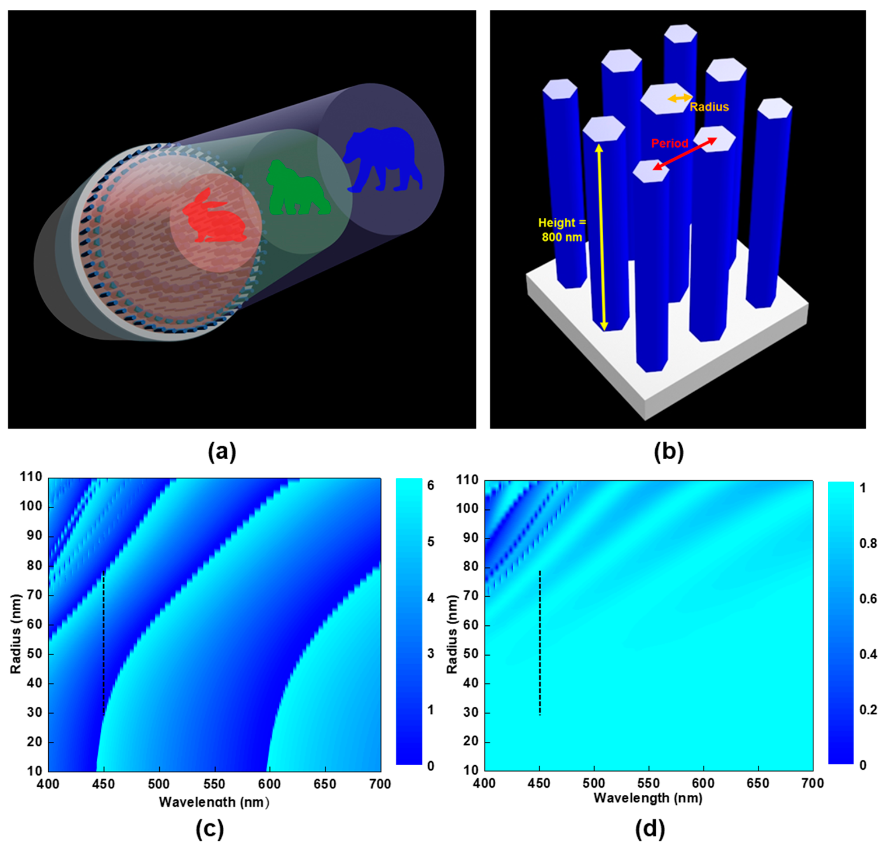
2. Design and Fabrication of the Metalens

Figure 1a shows a schematic for illustrating the image decryption of the metalens, with HREs as their building blocks revealed in Figure 1b. The phase profile of the metalens at the 450-nm wavelength should follow a traditional converging lens as:
φ ( x , y ) = 2 π λ ( f - x 2 + y 2 + f 2 )
where x and y are coordinates in connection with the center of the metalens surface with the focal distance f. λ is the free-space wavelength. The phase distribution is imparted by modifying the radii of the HREs. A commercially available CST software has been employed to optimize the efficiency of the HRE with respect to the required phase shift. With the selected subwavelength period of 220 nm, the CST-simulated phase shifts and efficiencies of the HREs are, respectively, shown in Figure 1c,d, in which the black dashed lines are radii of the HREs used for building up the metalens at the wavelength of 450 nm. The radius range corresponding to the dashed lines in the figure is between 28 and 76 nm. The simulation results show that near-unity transmission efficiency can be achieved by carefully choosing the HRE radii according to the chosen subwavelength period.
The 450 nm metalens was fabricated with a lens diameter of 100 μm and a focal length of 150 μm, producing a numerical aperture (NA) of 0.3. The fabrication processes start with the growth of an 800-nm-thick GaN epi-layer on a sapphire substrate using the metal-organic chemical vapor deposition (MOCVD), followed by depositing a 400 nm-thick silicon dioxide (SiO2) layer on the epi-ready substrate by the reactive-ion etching (RIE) system. The next step is coating a resist layer on the SiO2-deposited substrate. The subsequent processes are evaporating a 45 nm-thick chromium (Cr) layer on the developed resist-coated substrate after exposing a highly concentrated electron beam onto the top surface of the resist. The inductively coupled-plasma reactive-ion etching (ICP-RIE) is used to transfer the HRE patterns from the lift-off substrate to the GaN epi-layer. The metalens fabrication is completed after dipping the sample into a buffered oxide etchant (BOE) solution.
An optical microscope (OM) image of the fabricated metalens is shown in Figure 2a. The zoom-in secondary electron microscope (SEM) top-view images are represented in Figure 2b–d, which are individually associated with the color-dashed squares located in Figure 2a. The corresponding tilt-view SEM images are also provided in Figure 2e,f. It is worthwhile to note that the smallest radius of the HRE fabricated in the metalens is 28 nm, which is very challenging for the top-down approach to achieve such high-aspect ratio HREs with near-vertical sidewall morphology.

3. Image Decryption by Metalens and Discussion

Figure 3a displays a schematic for the measurement setup to experimentally demonstrate the image decryption capability for the metalens. A commercialized projector using the white LED as a light source passes through a pinhole with a diameter of 100 μm along the z-axis, which is then focused by the metalens. Subsequently, the CMOS camera captures the experimentally decrypted images, which are obtained through a 20× objective used to collect the metalens-focused light beam.
To carefully ensure the encrypted images formed at the correct z-axis positions, the white LED in Figure 3a was replaced by two distinct lasers with respective peak emission wavelengths of 633 and 532 nm. The vertical cut of focal spot intensity distribution corresponding to the 633 and 532 nm incident lasers are, respectively, indicated in Figure 3b,c. The metalens illuminated with green laser possesses a focal length of 123 μm, while the red laser irradiating the metalens makes the focal distance become 87 μm.
For the proof of concept, Figure 3d–f exhibit simple encrypted images to carry out the decryption experiment for the metalens. Each image is synthesized from three different red, green, and blue images based on the principle of color superposition. Figure 3g–i are the decrypted images that are acquired at the length of 87-μm on the z-axis, resulting from the metalens irradiated with the projector. Obviously, only the images colored in red can be clearly revealed such as the dotted and solid capital letter R, respectively, shown in Figure 3g,h along with the rabbit in Figure 3i. On the other hand, one needs to increase the z-axis distance up to 123 μm in order to decrypt the green images as demonstrated in Figure 3j–l. It is also predictable to make blue image decryption available by moving the z-axis length to 150 μm, the focal distance of the metalens with 450-nm laser as incident irradiation as displayed in Figure 3m–o. It is worth noting that the blurred edges found in the images because the metalens is designed at the specific wavelength of 450 nm and illuminated with the white LED light source operating over a continuous wavelength regime at visible. These images can be further improved by designing metalenses capable of broadband achromatic operation or by inserting a bandpass filter with a narrow bandwidth in the measurement setup.
Although the concept of image encryption proposed in this study seems simple, the image decryption becomes more complicated by adding numbers of different color images. It is worthy of noting that the light generated by the white LED traveling through a 100-µm-diameter pinhole can be spatially dispersed by the metalens based on the PB-phase design method to show a rainbow-like distribution as demonstrated in the literature [30], promising plenty of color options due to the wavelengths distributed continuously in the visible spectrum.

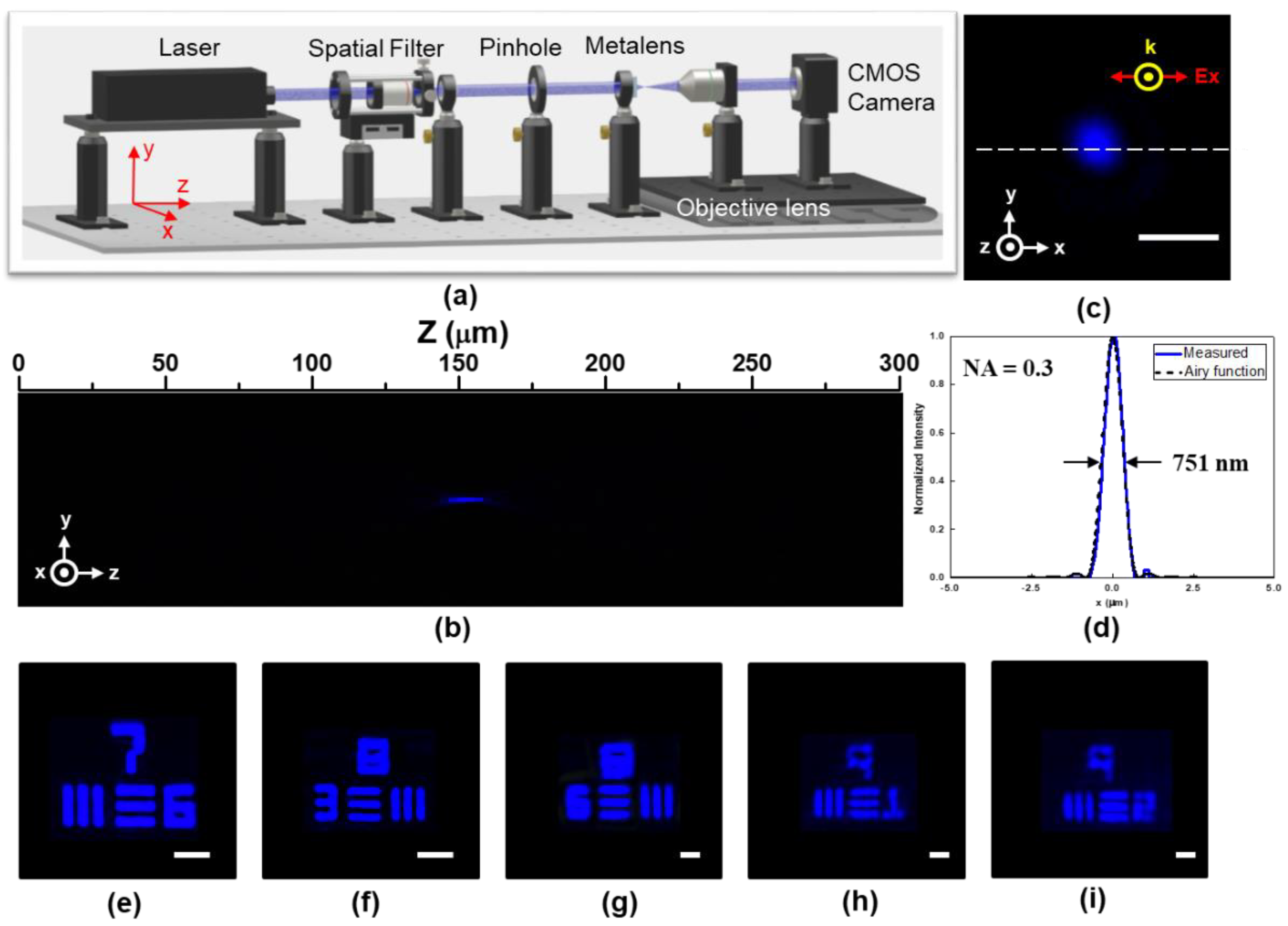
4. Metalens Characteristics

To carefully confirm the performance of the fabricated metalens, Figure 4a schematically depicts the measurement setup for the focal spot distribution and focusing efficiency of the fabricated metalens with an incident light source being a 450-nm diode laser, linearly polarized along the x-direction. This setup uses a spatial filter to eliminate speckles of the laser incidence to generate a pure Gaussian beam, succeeded by a 100-μm-diameter pinhole to reduce its beam spot. The highly concentrated beam spot is then produced by the metalens focusing. The CMOS camera and the objective lens are continuously moved together along the laser propagation direction to acquire x-y plane images at different z-axis positions. The cross-sectional light intensity profile (y-z plane) is further obtained by merging those captured x-y plane images as shown in Figure 4b. As shown in the figure, the measured focal spot is kept brightest at the z-axis position of 150 μm that is consistent with the designed focal length, showing an excellent light-converging of the fabricated metalens.
The x-y plane focal spot profile and the correlated cross-section of the metalens are, respectively, demonstrated in Figure 4c,d, in which a black-dashed line referring to the ideal Airy function. Experimental measurements show that the highly symmetrical focal spot has a cross-sectional profile very close to the ideal Airy function. The full-width at half-maximum (FWHM) of the metalens is 751 nm, which is extremely close to the theoretical value of the diffraction limit. The calculated formula can be found in the literature [23,24,28,29]. Moreover, the focusing efficiency is numerically calculated as high as 92% by the CST software using a metalens with the same NA of 0.3, but with a smaller diameter of 8 μm due to our computational limitation. The experimentally diffraction-limited focusing efficiency of the metalens is measured up to 88%. The efficiency is evaluated by the ratio of the optical power measured by the metalens with the diffraction-limited focusing to the laser light incident power going through a double-polished sapphire substrate together with a pinhole possessing a diameter in accordance with the metalens size.
The metalens imaging evaluation is characterized by choosing 1951 USAF as the imaging target. The setup of the measurement is similar to Figure 4a, except that the 1951 USAF target is additionally placed between the pinhole and the metalens. As shown in Figure 4e–i, all of the features can be clearly identified and distinguished. The smallest line width resolved in the figures is as low as 870 nm, with line separation by a center-to-center distance of 1.74 μm. The experimental imaging results elucidate the successful manufacturing of the high-performance metalens comprised of high-aspect-ratio HREs.

5. Conclusions

In this work, we have successfully demonstrated images decrypted by the fabricated metalens. The encrypted images can be clearly observed at appropriate z-axis positions, which are carefully inspected by using the lasers as incident light sources. The metalens proposed in this study is capable of polarization-insensitive focusing of diffraction limit with efficiency up to 88%. Additionally, the smallest line with the width of 870 nm in the 1951 USAF can be clearly observed. Such a polarization-insensitive metalens of high performance is constructed with HREs. This work provides another application for metalenses and paves the way for the research community to explore other advances in secure digital data by metalenses.

Author Contributions

Conceptualization, M.-H.C. and V.-C.S.; methodology, M.-H.C. and V.-C.S.; software, M.-H.C.; validation, M.-H.C., J.-Y.L. and V.-C.S.; formal analysis, M.-H.C., J.-Y.L. and V.-C.S.; investigation, M.-H.C. and V.-C.S.; resources, V.-C.S.; data curation, M.-H.C., J.-Y.L. and V.-C.S.; writing—original draft preparation, M.-H.C. and V.-C.S.; writing—review and editing, M.-H.C. and V.-C.S.; visualization, M.-H.C. and V.-C.S.; supervision, M.-H.C. and V.-C.S.; project administration, M.-H.C. and V.-C.S.; funding acquisition, V.-C.S. All authors have read and agreed to the published version of the manuscript.

Funding

This research was funded by the Ministry of Science and Technology, Taiwan, grant number MOST 109-2221-E-239-016-, MOST 110-2221-E-239-026-MY3.

Data Availability Statement

The data regarding the findings of this study are available from the corresponding author.

Conflicts of Interest

The authors declare no conflict of interest.

References

  1. Li, Z.F.; Dong, G.Y.; Yang, D.Y.; Li, G.L.; Shi, Y.S.; Bi, K.; Zhou, J. Efficient dielectric metasurface hologram for visual-cryptographic image hiding. Opt. Express 2019, 27, 19212–19217. [Google Scholar] [CrossRef] [PubMed]
  2. Luo, X.H.; Hu, Y.Q.; Li, X.; Jiang, Y.T.; Wang, Y.S.; Dai, P.; Liu, Q.; Shu, Z.W.; Duan, H.G. Integrated Metasurfaces with Microprints and Helicity-Multiplexed Holograms for Real-Time Optical Encryption. Adv. Opt. Mater. 2020, 8, 9. [Google Scholar] [CrossRef]
  3. Lin, C.; Han, Y.L.; Lou, S.L.; Li, Z.Y. High spectral and spatial resolved encryption and decryption of 3D color object based on holographic imaging spectroscopy. Opt. Lasers Eng. 2021, 145, 8. [Google Scholar] [CrossRef]
  4. Song, Q.H.; Khadir, S.; Vezian, S.; Damilano, B.; de Mierry, P.; Chenot, S.; Brandli, V.; Laberdesque, R.; Wattellier, B.; Genevet, P. Printing polarization and phase at the optical diffraction limit: Near- and far-field optical encryption. Nanophotonics 2021, 10, 697–704. [Google Scholar] [CrossRef]
  5. Zheng, P.X.; Dai, Q.; Li, Z.L.; Ye, Z.Y.; Xiong, J.; Liu, H.C.; Zheng, G.X.; Zhang, S. Metasurface-based key for computational imaging encryption. Sci. Adv. 2021, 7, 7. [Google Scholar] [CrossRef]
  6. Chowdhary, C.L.; Patel, P.V.; Kathrotia, K.J.; Attique, M.; Perumal, K.; Ijaz, M.F. Analytical Study of Hybrid Techniques for Image Encryption and Decryption. Sensors 2020, 20, 5162. [Google Scholar] [CrossRef] [PubMed]
  7. Shen, Z.; Teo, C.Z.W.; Ayyer, K.; Loh, N.D. An encryption-decryption framework to validating single-particle imaging. Sci. Rep. 2021, 11, 17. [Google Scholar] [CrossRef]
  8. Yu, N.; Capasso, F. Flat optics with designer metasurfaces. Nat. Mater. 2014, 13, 139–150. [Google Scholar] [CrossRef]
  9. Jahani, S.; Jacob, Z. All-dielectric metamaterials. Nat. Nanotechnol. 2016, 11, 23–36. [Google Scholar] [CrossRef]
  10. Hsiao, H.-H.; Chu, C.H.; Tsai, D.P. Fundamentals and Applications of Metasurfaces. Small Methods 2017, 1, 1600064. [Google Scholar] [CrossRef] [Green Version]
  11. Lalanne, P.; Chavel, P. Metalenses at visible wavelengths: Past, present, perspectives. Laser Photonics Rev. 2017, 11, 1600295. [Google Scholar] [CrossRef]
  12. Su, V.C.; Chu, C.H.; Sun, G.; Tsai, D.P. Advances in optical metasurfaces: Fabrication and applications invited. Opt. Express 2018, 26, 13148–13182. [Google Scholar] [CrossRef] [PubMed]
  13. Yu, N.F.; Genevet, P.; Kats, M.A.; Aieta, F.; Tetienne, J.P.; Capasso, F.; Gaburro, Z. Light Propagation with Phase Discontinuities: Generalized Laws of Reflection and Refraction. Science 2011, 334, 333–337. [Google Scholar] [CrossRef] [PubMed] [Green Version]
  14. Chen, X.; Huang, L.; Muhlenbernd, H.; Li, G.; Bai, B.; Tan, Q.; Jin, G.; Qiu, C.W.; Zhang, S.; Zentgraf, T. Dual-polarity plasmonic metalens for visible light. Nat. Commun. 2012, 3, 1198. [Google Scholar] [CrossRef] [PubMed]
  15. Yu, N.; Aieta, F.; Genevet, P.; Kats, M.A.; Gaburro, Z.; Capasso, F. A broadband, background-free quarter-wave plate based on plasmonic metasurfaces. Nano Lett. 2012, 12, 6328–6333. [Google Scholar] [CrossRef]
  16. Hsu, W.L.; Wu, P.C.; Chen, J.W.; Chen, T.Y.; Cheng, B.H.; Chen, W.T.; Huang, Y.W.; Liao, C.Y.; Sun, G.; Tsai, D.P. Vertical split-ring resonator based anomalous beam steering with high extinction ratio. Sci. Rep. 2015, 5, 11226. [Google Scholar] [CrossRef] [Green Version]
  17. Fu, Y.H.; Kuznetsov, A.I.; Miroshnichenko, A.E.; Yu, Y.F.; Luk’yanchuk, B. Directional visible light scattering by silicon nanoparticles. Nat. Commun. 2013, 4, 1527. [Google Scholar] [CrossRef] [Green Version]
  18. Zywietz, U.; Evlyukhin, A.B.; Reinhardt, C.; Chichkov, B.N. Laser printing of silicon nanoparticles with resonant optical electric and magnetic responses. Nat. Commun. 2014, 5, 3402. [Google Scholar] [CrossRef]
  19. Park, J.S.; Zhang, S.Y.; She, A.; Chen, W.T.; Lin, P.; Yousef, K.M.A.; Cheng, J.X.; Capasso, F. All-Glass, Large Metalens at Visible Wavelength Using Deep-Ultraviolet Projection Lithography. Nano Lett. 2019, 19, 8673–8682. [Google Scholar] [CrossRef]
  20. Khorasaninejad, M.; Chen, W.T.; Devlin, R.C.; Oh, J.; Zhu, A.Y.; Capasso, F. Metalenses at visible wavelengths: Diffraction-limited focusing and subwavelength resolution imaging. Science 2016, 352, 1190–1194. [Google Scholar] [CrossRef] [Green Version]
  21. Chen, W.T.; Zhu, A.Y.; Sisler, J.; Bharwani, Z.; Capasso, F. A broadband achromatic polarization-insensitive metalens consisting of anisotropic nanostructures. Nat. Commun. 2019, 10, 7. [Google Scholar] [CrossRef] [Green Version]
  22. Chen, W.T.; Zhu, A.Y.; Sanjeev, V.; Khorasaninejad, M.; Shi, Z.J.; Lee, E.; Capasso, F. A broadband achromatic metalens for focusing and imaging in the visible. Nat. Nanotechnol. 2018, 13, 220–226. [Google Scholar] [CrossRef] [PubMed] [Green Version]
  23. Chen, B.H.; Wu, P.C.; Su, V.C.; Lai, Y.C.; Chu, C.H.; Lee, I.C.; Chen, J.W.; Chen, Y.H.; Lan, Y.C.; Kuan, C.H.; et al. GaN Metalens for Pixel-Level Full-Color Routing at Visible Light. Nano Lett. 2017, 17, 6345–6352. [Google Scholar] [CrossRef] [PubMed]
  24. Chen, M.H.; Chou, W.N.; Su, V.C.; Kuan, C.H.; Lin, H.Y. High-performance gallium nitride dielectric metalenses for imaging in the visible. Sci. Rep. 2021, 11, 6500. [Google Scholar] [CrossRef]
  25. Zang, X.F.; Xu, W.W.; Gu, M.; Yao, B.S.; Chen, L.; Peng, Y.; Xie, J.Y.; Balakin, A.V.; Shkurinov, A.P.; Zhu, Y.M.; et al. Polarization-Insensitive Metalens with Extended Focal Depth and Longitudinal High-Tolerance Imaging. Adv. Opt. Mater. 2020, 8, 9. [Google Scholar] [CrossRef]
  26. Li, L.; Liu, Z.X.; Ren, X.F.; Wang, S.M.; Su, V.C.; Chen, M.K.; Chu, C.H.; Kuo, H.Y.; Liu, B.H.; Zang, W.B.; et al. Metalens-array-based high-dimensional and multiphoton quantum source. Science 2020, 368, 1487–1490. [Google Scholar] [CrossRef] [PubMed]
  27. Lin, R.J.; Su, V.C.; Wang, S.M.; Chen, M.K.; Chung, T.L.; Chen, Y.H.; Kuo, H.Y.; Chen, J.W.; Chen, J.; Huang, Y.T.; et al. Achromatic metalens array for full-colour light-field imaging. Nat. Nanotechnol. 2019, 14, 227–231. [Google Scholar] [CrossRef]
  28. Wang, S.M.; Wu, P.C.; Su, V.C.; Lai, Y.C.; Chen, M.K.; Kuo, H.Y.; Chen, B.H.; Chen, Y.H.; Huang, T.T.; Wang, J.H.; et al. A broadband achromatic metalens in the visible. Nat. Nanotechnol. 2018, 13, 227–232. [Google Scholar] [CrossRef] [PubMed]
  29. Chen, M.H.; Yen, C.W.; Guo, C.C.; Su, V.C.; Kuan, C.H.; Lin, H.Y. Polarization-insensitive GaN metalenses at visible wavelengths. Sci. Rep. 2021, 11, 14541. [Google Scholar] [CrossRef]
  30. Su, V.C.; Gao, C.C. Remote GaN metalens applied to white light-emitting diodes. Opt. Express 2020, 28, 9. [Google Scholar] [CrossRef]
Figure 1. (a) Schematic describing a digital image decrypted by a metalens; (b) schematic showing the building blocks of the metalens; (c) the diagram referring to the phase modulation of the building blocks; and (d) simulated efficiencies corresponding to the building blocks.
Crystals 11 01320 g001
Figure 2. (a) The OM image of the fabricated metalens, scale bar: 10 μm; (bd) top-view SEM images associated the color-dashed squares in (a), scale bar: 500 nm; and (e,f) tilt-view SEM images associated the color-dashed squares in (a), scale bar: 500 nm.
Crystals 11 01320 g002
Figure 3. (a) Schematic for the setup of the image decryption by the metalens; the cross-sectional intensity distribution using 633 and 532 nm laser as the light incidence, respectively, shown in (b,c); (df) the encrypted images produced by the projector; (gi) the decrypted images with the dotted and solid red capital letter R in (g,h), respectively, together with a red rabbit in (i); (jl) the decrypted images with the dotted and solid green capital letter G in (j,k), respectively, together with a green gorilla in (l); and (mo) the decrypted images with the dotted and solid blue capital letter B in (m,n), respectively, together with a blue bear in (o); Scale bar: 10 μm in (go).
Crystals 11 01320 g003
Figure 4. (a) Schematic for illustrating the measurement setup for diffraction-limited focusing; (b) the y-z plane cross-sectional image; (c) measured focal spot profile (x-y plane); (d) the cross-sectional intensity distribution of the focal spot, with the dashed line indicating the ideal Airy function; and (ei) the measured images using 1951 USAF as the target, scale bar: 10 μm in (e,f), scale bar: 3 μm in (gi).
Crystals 11 01320 g004
Publisher’s Note: MDPI stays neutral with regard to jurisdictional claims in published maps and institutional affiliations.

