Hardness, Young’s Modulus and Elastic Recovery in Magnetron Sputtered Amorphous AlMgB14 Films


1
Division of Electronics and Embedded Systems, School of Electrical Engineering and Computer Science, KTH Royal Institute of Technology, SE-164 40 Stockholm-Kista, Sweden
2
INMATECH Intelligent Materials Technology, SE-127 51 Skärholmen, Sweden
3
Petrozavodsk State University, 185910 Petrozavodsk, Russia
Crystals 2020, 10(9), 823; https://doi.org/10.3390/cryst10090823
Submission received: 24 August 2020
/
Revised: 9 September 2020
/
Accepted: 15 September 2020
/
Published: 16 September 2020
(This article belongs to the Special Issue Hardmetal)
Abstract
:We report optical and mechanical properties of hard aluminum magnesium boride films magnetron sputtered from a stoichiometric AlMgB14 ceramic target onto Corning® 1737 Glass and Si (100) wafers. High target sputtering rf-power and sufficiently short target-to-substrate distance appeared to be critical processing conditions. Amorphous AlMgB14 films demonstrate very strong indentation size effect (ISE): exceptionally high nanohardness H = 88 GPa and elastic Young’s modulus = 517 GPa at 26 nm of the diamond probe penetration depth and almost constant values, respectively, of about 35 GPa and 275 GPa starting at depths of about 2–3% of films’ thickness. For comparative analysis of elastic strain to failure index , resistance to plastic deformation ratio and elastic recovery ratio were obtained in nanoindentation tests performed in a wide range of loading forces from 0.5 to 40 mN. High authentic numerical values of H = 50 GPa and = 340 GPa correlate with as low as only 10% of total energy dissipating through the plastic deformations.
1. Introduction
For the first time, aluminum magnesium boride was sintered in 1970 in Carborundum Company by V.I. Matkovich and J. Economy. Small black AlMgB14 crystals were prepared by heating a mixture of aluminum, magnesium and boron at a temperature of 900 °C. Their structure was determined as a 3D network formed from icosahedral B12 groups within the orthorhombic unit cell with the dimensions a = 10.313 Å, b = 8.115 Å, and c = 5.848 Å [1]. Results obtained in succeeding works on AlMgB14 can be divided into three main groups. True stoichiometry Al0.75Mg0.78B14, thermoelectric, electronic and optical properties were reported between the 1970s and 1990s (see references in Ref. [2]). Next, in 1993 Higashi et al. and later in 2000 Cook et al. from Iowa have reported exceptional hardness of AlMgB14 crystals as high as, respectively, 27.4–28.3 GPa [3] and 32–35 GPa [2]. Lastly in 2003, the same Iowa group took an important step in exploration of AlMgB14 fabricating superhard self-lubricating (hereinafter BAM) films. They used pulsed laser deposition (PLD) technique to obtain films which hardness ranged from 45 to 51 GPa [4].
Recently, we succeeded in deposition of high quality amorphous BAM films by an RF magnetron sputtering method which can easily be scaled up for industrial use. High sputtering power of ceramic AlMgB14 target, moderately low substrate temperature, and a short target-to-substrate distance enabled high-energy ballistic impact regime of adatoms’ motion thus leading to an enhanced hardness by 25% and Young’s modulus by 60%, compared to PLD-made films. Correct stoichiometry and compositional in-depth homogeneity governed superior mechanical properties of magnetron sputtered films [5]. Correlative theoretical and experimental elaboration of high power pulsed magnetron sputtering (HPPMS) of AlYB14 films acknowledged the ability to form icosahedral boron-rich phases below the bulk synthesis temperatures [6]. Matching results of ab initio molecular dynamics calculations of elastic properties with nanoindentation measurements of Young’s modulus proved the predictive power of the HPPMS technique to sinter amorphous boride coatings [7].
Both amorphous AlMgB14 films obtained by pulsed laser deposition [4] and magnetron sputtering [5] exhibit a strong indentation size effect (ISE). This is the exceptionally high parameters of nanohardness H and elastic Young’s modulus at the tens-of-nanometer-scale of penetration depth of a diamond probe and their very steep decrease to the constant values at depths of about 2–3% of the film’s thickness. Still the general necessity remains to authenticate these results. Herein, we examined additional mechanical parameters: elastic strain to failure index , resistance to plastic deformation ratio , and elastic recovery ratio . Maximum values of calculated parameter and measured as high as 90% always match the peak values of hardness H and elastic modulus . Therefore, we relate ISE to a very low portion of total energy dissipating through the plastic deformations at shallow indenter prints.
2. Materials and Methods
The details of RF magnetron sputtering of ultra-hard AlMgB14 coatings were published elsewhere [5]. In brief, a batch of BAM films was deposited onto Si(100) wafers and Corning® 1737 glass by sputtering of a stoichiometric AlMgB14 ceramic target. The target was manufactured via the grinding and subsequent spark plasma sintering of Al (99.97%), Mg (99.8%), and B (99%) powders [8]. The ultimate pressure in vacuum chamber was better than 3 × 10⁻⁷ Torr, films deposition was carried out at 7 mTorr of Ar-gas pressure. In-depth uniformity, smooth surface and ultimate hardness of BAM films were achieved at optimum processing conditions: distance of 25 mm between 1 inch 50 W RF powered magnetron and substrates kept on the heater at 250–350 °C. Typical film size was 10 × 10 mm2, deposition rate was 0.44 nm/s. Films’ roughness was checked with KLA-Tencor P-15 stylus profiler. It does not exceed the roughness of Corning® 1737 glass and Si wafers as the substrates.
All films sintered at different temperatures varied from room temperature up to 550 °C and appeared to be X-ray amorphous. BAM films onto Si wafers do not exhibit themselves with any XRD pattern (recorded with a Siemens D-5000 powder diffractometer) even in a magnifying log-scale. Θ-2Θ scan of 0.4 μm thick BAM/Si film in the main frame of Figure 1 contains only Si(100) wafer’s Bragg reflections. In insets, the selected area electron diffraction (SAED, performed on a FEI Tecnai T20 TEM) pattern and HRTEM image also attest amorphous structure of 2.12-μm-thick BAM/Si film.
Optical dispersion was evaluated from the transmission spectrum of BAM films onto glass substrate recorded at normal light incidence with a Fourier transform infrared spectrometer Nicolet 5700 in the range 0.3–2.5 μm. The spectrum was normalized to the spectrum of the bare glass substrate. Unpolarized backscattered micro-Raman spectra of AlMgB14 films onto Si(100) wafers were collected with a confocal Thermo Scientific Nicolet Almega XR Dispersive Raman Spectrometer at room temperature using 785 nm and 532 nm laser pumping. NHT S/N 06-0134 and TTX-NHT2 S/N 01-05821 nanoindentation instruments with Berkovich three-sided diamond pyramid tips were employed to measure hardness H and effective Young’s modulus . In calculation we used ν = 0.25 as a Poisson’s ratio for AlMgB14 films. Abrasion BAM films’ properties were characterized using CSM Instruments SA micro-scratch tester S/N 01-03079 with the diamond Rockwell C indenter of 200-μm radius.
3. Results and Discussion
3.1. Optical Properties
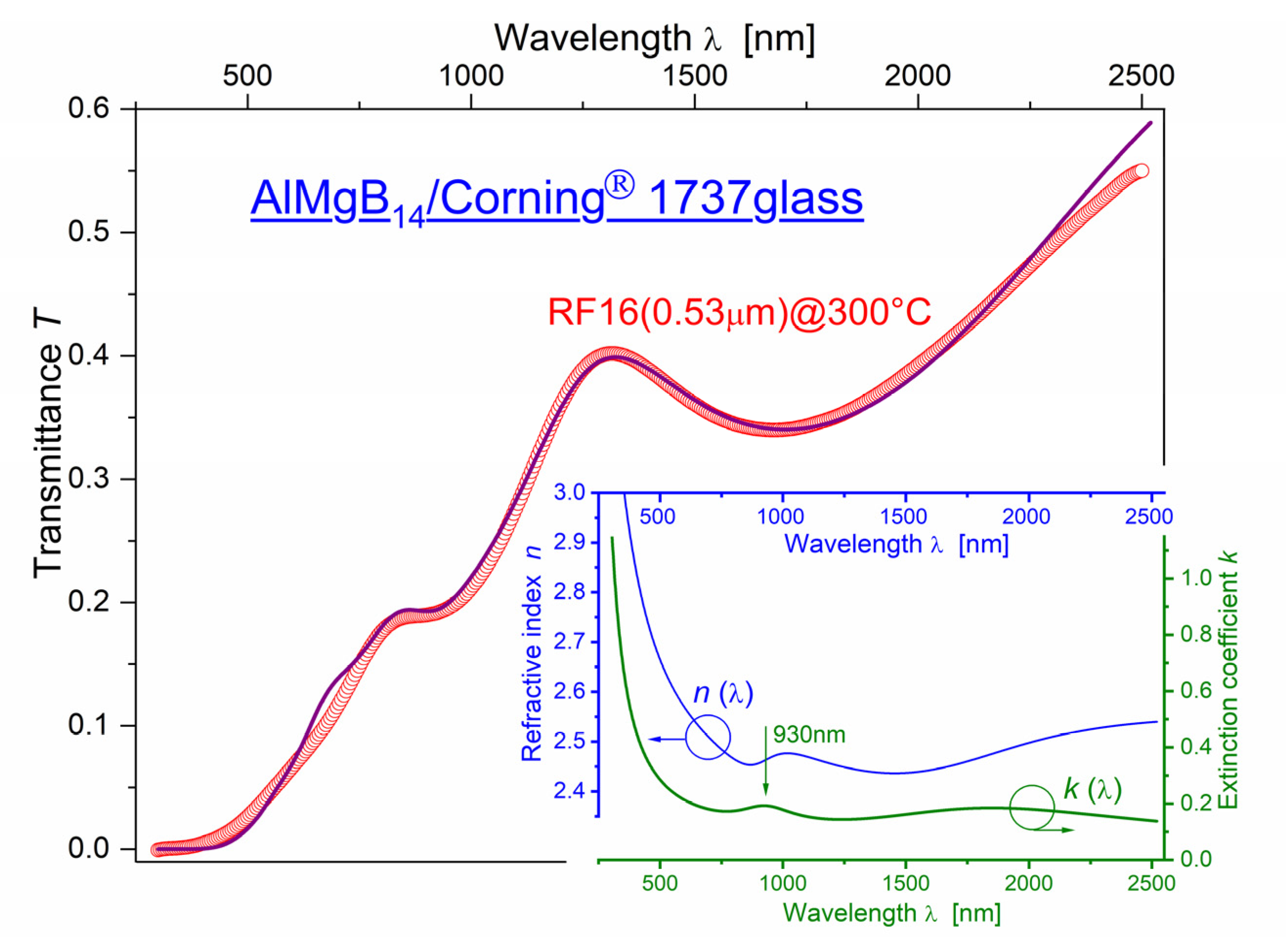
Circular symbols in Figure 2 display optical transmission spectrum of 0.53-μm-thick film onto transparent Corning® 1737 glass substrate. It has a semiconductor-type character. The absorption edge lies around 310 nm (bandgap is 4 eV) and specific resistivity .
Observed spectrum features we modeled with a commonly used Swanepoel [9] formula (follows afterward in Appendix A). Theoretical solid line in Figure 2 firmly fits to the experimental spectrum. A good agreement with the experimental results was achieved presenting complex refractive index with three Sellmeier-type electric dipole resonances, Equation (1):
Inset to Figure 2 shows a wavelength dispersion of refractive index n(λ) and extinction coefficient k(λ) calculated with Equation (1). Within the explored 0.3–2.5 μm range, they distinctly reveal dipole resonance at 930 nm. It manifests itself as a hump in extinction coefficient k(λ) and as a derivative-type curve of the real part of refractive index n(λ) correspondent to Kramers–Kronig relations.
Figure 3 presents unpolarized backscattered micro-Raman spectra for two RF15-2(2.12 μm) and RF11(0.88 μm) BAM films prepared onto Si(100), respectively, at 250 °C and 300 °C. Red/magenta and green/cyan color symbols depict spectra obtained at 785 nm and 532 nm laser light pumping, correspondingly.
Since the structure of AlMgB14 films is completely amorphous, the Raman spectra do not contain any narrow lines. There are two broad bands with maxima at 1128 cm−1 and 1260 cm−1. Following Ref. [10] we attribute them, respectively, to intra-icosahedral B-B vibration Eg modes and to predominantly inter-icosahedral B-B vibration A1g modes. The shoulder around 840 cm−1 and the broad band ranging from 1030 up to 2000 cm−1 can rely upon Raman and IR active vibrations in the molecule of orthorhombic boric acid [11]. Molecular vibrations of boric acid together with Eg and A1g icosahedral B-B vibrational modes can be ascribed to the subtle optical resonance absorption at λ = 930 nm revealed in inset to Figure 2.
Three (OH)−1 groups surround B3+ atom and form a planar trigonal molecular configuration. Strong hydrogen bonds between hydroxyl groups build a stable layer of B(OH)3 molecules whereas only weak van der Waal’s forces link two adjacent layers to each other at the distance of 0.318 nm. Easily sheared multilayered B(OH)3 structure governs unique lubrication properties of crystalline boric acid [12]. These nanometer-thick B(OH)3 surface layers make BAM films slicker than Teflon TM [13]. Mechanical properties of AlMgB14 films are not affected by boric acid since its hardness and elastic modulus are as low as 1.2 GPa and 15 GPa, correspondingly [14]. Due to ultra-high hardness and slipperiness, BAM films have great potential for a wide range of diverse applications for MEMS devices, wear-resistant and low-friction transparent coatings, metal dies, measuring tools and gauges.
3.2. Nanoindentation
Nanoindentation tests of AlMgB14 films on Si(100) wafers were conducted applying a load to Berkovich diamond pyramid tip from 0.5 up to 40 mN. The measurements were carried out applying a multiple simple matrix 2×2 indentations to exclude spurious notches and collect reliable data sufficient for statistical averaging. A new diamond probe adjustment was performed every time for the next 2×2 indentations. To eliminate a role of Si substrate, penetration depth of the diamond indenter did not exceed 10–15% of films’ thickness. Typical loading L(h) (ascending) and unloading L↓(h) (descending) force curves are shown in Figure 4. The area between the loading and unloading curve represents the energy dissipated in BAM film due to plastic deformation whereas the area under the unloading curve defines recovered work of elastic forces.
Load-displacement curves are used to determine three main parameters that characterize hard AlMgB14 films: hardness H, effective Young’s modulus and elastic recovery ratio . H and are calculated as per the Oliver and Pharr method fitting L↓(h) = A(h − hres)m dependence to the experimental unloading force curve [15]. Elastic recovery ratio is defined as a ratio of areas under unloading L↓(h) and loading L↑(h) curves, Equation (2):
From ascertained values of H and , we calculate dimensionless elastic strain index and the ratio measured in GPa. It is commonly assumed that a material with high ratio like 0.1 possesses a better wear resistance than a material with a low ratio . Parameter controls the resistance of the coating to plastic deformation. Really, to initiate plastic deformation, loading force should exceed the critical value [16]. Therefore, plasticity is reduced in materials with higher hardness and lower modulus. The next paragraph presents all the above mentioned mechanical parameters measured in BAM films at different loading forces.
3.3. Hardness and Young’s Modulus
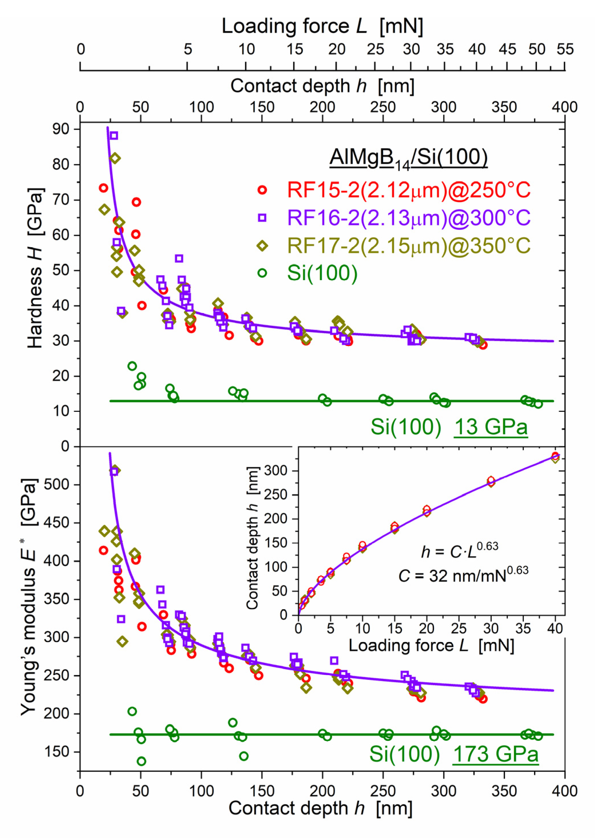
Symbols in Figure 5 present experimental data for hardness H and Young’s modulus collected for all the indentations made at different loading forces L in three AlMgB14 films fabricated within the optimal temperature range 250–350 °C.
Measurements performed at too shallow notches exhibit severe noise, seem much less reproducible and hence yield big scattering of H and data. To find reliable range of the loading force that guaranties authentic results, we have performed the nanohardness test of blank 300 μm thick Si(100) wafer used as a substrate for BAM films deposition (see results are also shown in Figure 5). At loading forces above 2 mN, both measured hardness 13 GPa and Young’s modulus 173 GPa are very close to the hardness H = 10.5–13 GPa and modulus = 130–185 GPa reported in the literature for different directions in Si single crystals [17,18,19]. Uncertain values of hardness δH = 10 GPa and modulus δE = ± 32 GPa obtained for Si serve as an estimate accuracy of indentation tests at weak loading forces. Despite big scattering of the data observed at shallow indentations, a strong indentation size effect (ISE) is readily seen in Figure 5. Both hardness H and modulus sharply increase at weak loads L ~ 0.5–2 mN (small h ~ 20–50 nm) reaching the peak values of 88 GPa and 517 GPa, correspondingly. At stronger loading forces 2–5 mN, H and data become less scattered and depth dependent. This “veritable” L interval starts from 2% and continues to 15% of the relative film thickness indenter’s penetration depth without any indication of Si substrate contribution to H and .
3.4. Plastic and Elastic Parts of the Indentation Work
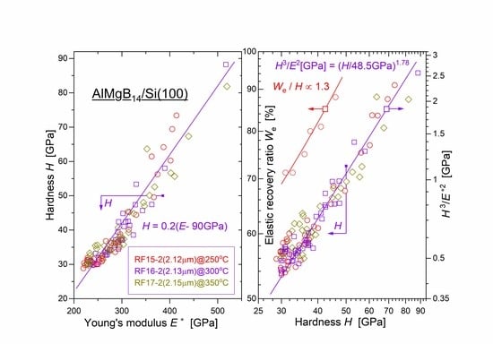
In Figure 6, we drew dependencies of the nanohardness H upon the elastic modulus , resistance to plastic deformation ratio and elastic recovery ratio vs. H obtained at different loading forces L. This plot composed of a complete set of the same, as in Figure 5, H and data.
For all three films grown at “favorable” 250–350 °C temperatures, hardness H vs. modulus data form the most dense track along the straight line for which the slope yields high a value of elastic strain index = 0.2. The dependence of resistance to plastic deformation ratio upon the nanohardness H follows the power law . High hardness is always accompanied with very high values of growing as to become higher than 90%.
When load weakens (L < 2 mN), scattering of H and data quickly grows. It happens because the energy dissipating through the plastic deformations suddenly decreases at shallow prints and the shape of load-displacement curves experiences severe distortions. Therefore, the most reliable results for elastic strain index and ratio are marked in Figure 6 with the straight lines pointed towards H < 50 GPa. Indentation size effect (ISE) manifests a strong reduction of the main mechanical parameters. It is readily seen in Figure 5 and Figure 6 when the penetration depth of a diamond probe h increasing from 28 to 330 nm. Namely: H becomes reduced by 66%, by 56%, resistance to plastic deformation ratio is diminished by 83%, and elastic recovery decreases from 90 ± 5% down to 71 ± 1%.
Strong ISE, wide spread of mechanical properties of BAM films and their correlation with hardness resemble results reported by J. Musil for nanocomposite titanium, zirconium and chromium nitride coatings sputtered at different deposition conditions [20,21]. Similar to AlMgB14, these films in an amorphous state exhibit superhardness , hardness and elastic modulus grow at weak loads whereas energy dissipating through the plastic deformations decreases ( increases up to about 85% for films with H ≈ 70 GPa), H(L) and values become constant at higher loads L demonstrating independence on substrate properties. In Figure 6, linear dependence and power law obtained for BAM films accord J. Musil’s conclusion on the general character of these relations for numerous oxides, carbides and nitrides prepared by magnetron sputtering under different deposition conditions [22].
Scratch tests performed with AlMgB14 films on Si(100) and Corning® 1737 glass substrates enable determination of the second critical loads Lc2 when side chips and peelings of coating appear inside the indenter’s track. Corresponding Lc2 values were used to obtain film-substrate interfacial adhesion strength equal to 18.4 J/m2 and 6.4 J/m2 for BAM film on Si(100) and glass substrate, correspondingly (see the details in Ref. [23] and [24]).
4. Conclusions
Optical properties of amorphous magnetron sputtered AlMgB14 films are characterized by constan in near IR values of refractive index n = 2.5 and extinction coefficient k = 0.2 as well as two bands of Raman-active intra- and inter-icosahedral boron–boron vibrations. Nanoindentation tests displayed a strong indentation size effect (ISE): exceptionally high values of hardness H and Young’s modulus at the tens-of-nm-scale of indenter penetration depth and a very steep decrease to almost constant parameters at depths which are only 2–3% of films’ thickness. Peak values of H and correspond to the maximum values of calculated resistance to plastic deformation ratio and elastic recovery ratio . We arrived at the conclusion that ISE is a natural attribute of anomalous low energy dissipated through the plastic deformations at shallow indenter’s prints.
5. Patents
Funding
This research was partially supported within the Ministry of Science and Higher Education of the Russian Federation special assignment (No. 0752-2020-0007/AAAA-A20-120070290151-6).
Conflicts of Interest
The funders had no role in the design of the study; in the collection, analyses, or interpretation of data; in the writing of the manuscript, or in the decision to publish the results.
Appendix A
To model experimentally recorded optical transmittance spectrum, in Figure 2 we employed a commonly used Swanepoel [9] formula, Equation (A1):
Equation (A2) represents the wavelength-dependent coefficients:
Here n(λ), k(λ), and t are refractive index, extinction coefficient and thickness of AlMgB14 film, correspondingly, s(λ) is a substrate refractive index. We built the interpolation formula for the refractive index s(λ) of the Corning® 1737 glass, Equation (A3):
For this purpose, we used data for nine wavelengths presented at the vendor website [27]. They indicate 4.6% optical dispersion of the glass refractive index in the concerned range from 300 to 2500 nm.
References
- Matkovich, V.I.; Economy, J. Structure of MgAlB14 and a brief critique of structural relationships in higher borides. Acta Crystallogr. B 1970, 26, 616–621. [Google Scholar] [CrossRef]
- Cook, B.A.; Harringa, J.L.; Lewis, T.L.; Russel, A.M. A new class of ultra-hard materials based on AlMgB14. Scrip. Mater. 2000, 42, 597–602. [Google Scholar]
- Higashi, I.; Kobayashi, M.; Okada, S.; Hamano, K.; Lundström, T. Boron-rich crystals in Al-M-B (M = Li, Be, Mg) systems grown from high-temperature aluminum solutions. J. Cryst. Growth 1993, 128, 1113–1119. [Google Scholar] [CrossRef]
- Tian, Y.; Bastawros, A.F.; Lo, C.C.H.; Constant, A.P.; Russell, A.M.; Cook, B.A. Superhard self-lubricating AlMgB14 films for microelectromechanical devices. Appl. Phys. Lett. 2003, 83, 2781–2783. [Google Scholar] [CrossRef] [Green Version]
- Grishin, A.M.; Khartsev, S.I.; Böhlmark, J.; Ahlgren, M. Ultra-hard AlMgB14 coatings fabricated by RF magnetron sputtering from a stoichiometric target. JETP Lett. 2014, 100, 680–687. [Google Scholar]
- Hunold, O.; Chen, Y.-T.; Music, D.; Persson, P.O.Å.; Primetzhofer, D.; Baben, M.; Achenbach, J.-O.; Keuter, P.; Schneider, J.M. Correlative theoretical and experimental investigation of the formation of AlYB14 and competing phases. J. Appl. Phys. 2016, 119, 085307. [Google Scholar] [CrossRef] [Green Version]
- Hunold, O.; Keuter, P.; Bliem, P.; Music, D.; Wittmers, F.; Ravensburg, A.L.; Primetzhofer, D.; Schneider, J.M. Elastic properties of amorphous T0.75Y0.75B14 (T = Sc, Ti, V, Y, Zr, Nb) and the effect of O incorporation on bonding, density and elasticity (T’ = Ti, Zr). J. Phys. Cond. Matter 2017, 29, 085404. [Google Scholar]
- Roberts, D.J.; Zhao, J.; Munir, Z.A. Mechanism of reactive sintering of MgAlB14 by pulse electric current. Int. J. Refract. Met. Hard Mater. 2009, 27, 556–563. [Google Scholar] [CrossRef]
- Swanepoel, R. Determination of the thickness and optical constants of amorphous silicon. J. Phys. E Sci. Instrum. 1983, 16, 1214–1222. [Google Scholar] [CrossRef]
- Werheit, H.; Filipov, V.; Kuhlmann, U.; Schwarz, U.; Armbrüster, M.; Leithe-Jasper, A.; Tanaka, T.; Higashi, I.; Lundström, T.; Gurin, V.N.; et al. Raman effect in icosahedral boron-rich solids. Sci. Technol. Adv. Mater. 2010, 11, 023001. [Google Scholar]
- Goubeau, J.; Hummel, D. Die Schwingungsspektren verschiedener Borsauerstoffverbindungen. Z. Physik. Chem. N. F. 1959, 20, 15–33. [Google Scholar] [CrossRef]
- Choudhary, R.B.; Pande, P.P. Lubrication potential of boron compounds: An overview. Lubr. Sci. 2002, 14, 211–222. [Google Scholar] [CrossRef]
- Kleiner, K. Material Slicker than Teflon Discovered by Accident. NewScientist, Technology, 21 November 2008. Available online: https://www.newscientist.com/article/dn16102-material-slicker-than-teflon-discovered-by-accident/ (accessed on 16 September 2020).
- Music, D.; Kreissig, U.; Chirita, V.; Schneider, J.M.; Helmersson, U. Elastic modulus of amorphous boron suboxide thin films studied by theoretical and experimental methods. J. Appl. Phys. 2003, 93, 940–944. [Google Scholar] [CrossRef]
- Oliver, W.C.; Pharr, G.M. An improved technique for determining hardness and elastic modulus using load and displacement sensing indentation experiments. J. Mater. Res. 1992, 7, 1564–1583. [Google Scholar] [CrossRef]
- Tsui, T.Y.; Pharr, G.M.; Oliver, W.C.; Bhatia, C.S.; White, R.L.; Anders, S.; Anders, A.; Brown, I.G. Nanoindentation and nanoscratching of hard carbon coatings for magnetic discs. Mater. Res. Soc. Symp. Proc. 1995, 383, 447–452. [Google Scholar] [CrossRef] [Green Version]
- Bhushan, B.; Li, X. Micromechanical and tribological characterization of doped single-crystal silicon and polysilicon films for microelectromechanical systems devices. J. Mater. Res. 1997, 12, 54–63. [Google Scholar] [CrossRef]
- Ueda, M.; Lepienski, C.M.; Rangel, E.C.; Cruz, N.C.; Dias, F.G. Nanohardness and contact angle of Si wafers implanted with N and C and Al alloy with N by plasma ion implantation. Surf. Coat. Technol. 2002, 156, 190–194. [Google Scholar] [CrossRef]
- Hopcroft, M.A.; Nix, W.D.; Kenny, T.W. What is the Young’s modulus of silicon? J. Microelectromech. Syst. 2010, 19, 229–238. [Google Scholar] [CrossRef] [Green Version]
- Musil, J. Hard and superhard nanocomposite coatings. Surf. Coat. Technol. 2000, 125, 322–330. [Google Scholar] [CrossRef]
- Musil, J.; Kunc, F.; Zeman, H.; Poláková, H. Relations between hardness, Young’s modulus and elastic recovery in hard nanocomposite coatings. Surf. Coat. Technology 2002, 154, 304–313. [Google Scholar] [CrossRef]
- Musil, J.; Jirout, M. Toughness of hard nanostructured ceramic thin films. Surf. Coat. Technol. 2007, 201, 5148–5152. [Google Scholar] [CrossRef]
- Grishin, A.M. Abrasion resistant low friction and ultra-hard magnetron sputtered AlMgB14 coatings. Mater. Res. Express 2016, 3, 046402. [Google Scholar] [CrossRef]
- Putrolaynen, V.V.; Grishin, A.M.; Rigoev, I.V. Anti-Scratch AlMgB14 Gorilla® Glass Coating. Tech. Phys. Lett. 2017, 43, 871–874. [Google Scholar] [CrossRef]
- Putrolaynen, V.V.; Grishin, A.M.; Rigoev, I.V. Method for Fabrication of Wear Resistant Aluminum Magnesium Boride Coating. Patent RU 2677810, 7 March 2017. [Google Scholar]
- Putrolaynen, V.V.; Grishin, A.M.; Rigoev, I.V. Method for Fabrication of Transparent Wear Resistant Aluminum Magnesium Boride Coating on the Surface of Transparent Glassy Wares. Patent RU 2680548, 28 December 2017. [Google Scholar]
- Corning® 1737 AMLCD Glass Substrates. Material Information. Available online: http://www.vinkarola.com/pdf/Corning%20Glass%201737%20Properties.pdf (accessed on 16 September 2020).
Figure 1.
Main frame radiation of 0.4-μm-thick AlMgB14 film magnetron sputtered onto Si(100) wafer at 550 °C. Insets–XRD Θ-2Θ scan in ts: a–SAED pattern and b–high resolution TEM image of RF15-2(2.12 μm) AlMgB14 film grown onto Si(100) at 250 °C. Electron microscopy images provided courtesy of Dr. Jun Lu.

Figure 2.
Circular red color symbols show experimental optical transmittance T(λ) in 0.53-μm-thick AlMgB14 film grown at 300 °C onto the Corning® 1737 glass substrate. Solid lines in the main frame and inset depict, respectively, theoretical T(λ), refractive index n(λ) and extinction coefficient k(λ) simulated with the Swanepoel formula (see Appendix A) and Equation (1) for complex refractive index accounting for three electric dipole resonances.

Figure 3.
Unpolarized backscattered Raman spectra of two RF15-2(2.12 μm) and RF11(0.88 μm) AlMgB14 films grown onto Si(100) wafers, respectively, at 250 °C and 300 °C. Excitations at 785 nm (1.58 eV) and 532 nm (2.33 eV) laser light pumping are shown with red/magenta and green/cyan colors, correspondingly. Two vertical arrows mark Raman intra-icosahedral B-B vibration Eg band at 1128 cm−1 and inter-icosahedral B-B vibration A1g modes at 1260 cm−1. Raman and IR active vibrations in the molecule of orthorhombic boric acid B(OH)3 build the shoulder around 840 cm−1 and a broad 1030–2000 cm−1 band.

Figure 4.
Load-displacement curves of the hard RF15-2(2.12 μm) AlMgB14 film grown onto Si(100) substrate at 250 °C. Solid lines fit loading L↑(h) (ascending) and unloading L↓(h) (descending) experimental data shown with symbols. Area between L↑(h) and L↓(h) curves corresponds to plastic deformations whereas the colored section depicts the area of elastic recovery.

Figure 5.
Hardness H and elastic Young’s modulus dependencies upon contact depth h and loading force L measured in three different AlMgB14 films fabricated within the “favorable” temperature range 250–350 °C. Hardness H = 13 GPa and modulus = 173 GPa for a blank single crystal Si(100) wafer are shown for comparison. In inset, solid line is a power law h = C·L0.63 with C = 32 nm/mN0.63 fits experimental data for contact depth vs. loading force dependence.

Figure 6.
Left frame–hardness H vs. elastic modulus measured at different loading forces. Right frame–resistance to plastic deformation ratio and elastic recovery ratio vs. hardness H in the log-log scale.
Figure 6.
Left frame–hardness H vs. elastic modulus measured at different loading forces. Right frame–resistance to plastic deformation ratio and elastic recovery ratio vs. hardness H in the log-log scale.

© 2020 by the author. Licensee MDPI, Basel, Switzerland. This article is an open access article distributed under the terms and conditions of the Creative Commons Attribution (CC BY) license (http://creativecommons.org/licenses/by/4.0/).
Share and Cite
MDPI and ACS Style
Grishin, A.M. Hardness, Young’s Modulus and Elastic Recovery in Magnetron Sputtered Amorphous AlMgB14 Films. Crystals 2020, 10, 823. https://doi.org/10.3390/cryst10090823
AMA Style
Grishin AM. Hardness, Young’s Modulus and Elastic Recovery in Magnetron Sputtered Amorphous AlMgB14 Films. Crystals. 2020; 10(9):823. https://doi.org/10.3390/cryst10090823
Chicago/Turabian StyleGrishin, Alexander M. 2020. "Hardness, Young’s Modulus and Elastic Recovery in Magnetron Sputtered Amorphous AlMgB14 Films" Crystals 10, no. 9: 823. https://doi.org/10.3390/cryst10090823
Note that from the first issue of 2016, this journal uses article numbers instead of page numbers. See further details here.