Article

Optical Characterization of GaN-Based Vertical Blue Light-Emitting Diodes on P-Type Silicon Substrate

1
Center for Photonics and Semiconductors, School of Power and Mechanical Engineering, Wuhan University, Wuhan 430072, China
2
The Institute of Technological Sciences, Wuhan University, Wuhan 430072, China
3
Xiamen Changelight Co., Ltd., Xiamen 361000, China
4
State Key Laboratory of Applied Optics, Changchun Institute of Optics, Fine Mechanics and Physics, Chinese Academy of Sciences, Changchun 130033, China
*
Author to whom correspondence should be addressed.
Crystals 2020, 10(7), 621; https://doi.org/10.3390/cryst10070621
Submission received: 15 June 2020 / Revised: 10 July 2020 / Accepted: 13 July 2020 / Published: 16 July 2020
(This article belongs to the Special Issue GaN-Based Optoelectronic Materials and Light Emitting Devices)

Abstract

:
Fabricating GaN-based light-emitting diodes (LEDs) on a silicon (Si) substrate, which is compatible with the widely employed complementary metal–oxide–semiconductor (CMOS) circuits, is extremely important for next-generation high-performance electroluminescence devices. We conducted a systematic investigation of the optical properties of vertical LEDs, to reveal the impacts of the manufacturing process on their optical characteristics. Here, we fabricated and characterized high-efficiency GaN-based LEDs with integrated surface textures including micro-scale periodic hemispherical dimples and nano-scale random hexagonal pyramids on a 4 inch p-type Si substrate. The highly reflective Ag/TiW metallization scheme was performed to decrease downward-absorbing light. We demonstrated the influence of transferring LED epilayers from a sapphire substrate onto the Si substrate on the emission characteristics of the vertical LEDs. The removal of the sapphire substrate reduced the adverse impacts of the quantum-confined Stark effect (QCSE). The influence of integrated surface textures on the light extraction efficiency (LEE) of the vertical LEDs was studied. With the injection current of 350 mA, vertical LEDs with integrated surface textures demonstrated an excellent light output power of 468.9 mW with an emission peak wavelength of 456 nm. This work contributes to the integration of GaN-based vertical LEDs into Si-based integrated circuits.

1. Introduction

GaN-based light-emitting diodes (LEDs) have been proven to have great potentials as next-generation solid-state lighting due to their high color-rendering index, high efficiency, long life, compact size, and so forth [1,2,3]. However, further enhancements in optical performance for high-power LEDs are extremely important to penetrate general lighting and automotive front lighting markets [4,5,6]. The silicon (Si) substrate is compatible with the widely employed complementary metal–oxide–semiconductor (CMOS) circuits. The combination of GaN-based LEDs with Si-based integrated circuits would expedite the wide application of GaN-based LEDs [7].
Generally, the reported GaN-based LEDs can be categorized as follows: (1) Conventional top-emitting LED. The top-emitting LED is grown on a sapphire substrate. It is well known that large compressive strain exists in the GaN film due to the large lattice and thermal mismatch between the GaN film and sapphire substrate. This compressive strain causes a piezoelectric field in the InGaN/GaN multiple quantum wells (MQWs) and, thus, results in adverse impacts including fewer band-to-band transitions, fewer overlaps of the electron–hole wave functions, a red-shifted peak emission wavelength, and weakened radiative recombination, which is known as the quantum-confined Stark effect (QCSE) [8,9,10,11,12,13,14]. Due to the insulation of the sapphire substrate, both n- and p-type electrodes of a top-emitting LED are on the same side of the sapphire substrate. Thus, the current crowding effect (CCE) around the electrodes emerges, degrading device performance [15]. Moreover, the top-emitting LED suffers from a loss of active region area for the formation of n-contacts and poor thermal dissipation [16]. (2) Flip-chip LED. In the flip-chip LED configuration, the chip is inverted compared to conventional top-emitting LEDs. Light emits through the transparent sapphire substrate and, therefore, there is no attenuation of light by the semi-transparent metal electrode. In addition, the flip-chip LED can dissipate the heat generated in the active region through the thick metallization contacts. However, the flip-chip LED suffers from severe CCE occurring around the n-type electrode [17,18,19,20,21]. (3) Vertical LED. A GaN-based vertical LED is fabricated by transferring the LED epitaxial structure from a sapphire substrate onto a conductive substrate (such as Cu and Si). Compared to the top-emitting LED, the vertical LED has a larger emitting area without loss in active emitting region area, and the substrate with superior heat conductivity can improve the heat dissipation performance [22,23]. Compared to the flip-chip LED, the vertical configuration can effectively alleviate current crowding. With a superior device architecture, the vertical LED is considered more applicable for high-power and high-efficiency electroluminescence devices.
In the past few decades, many methods have been reported to develop a high-performance vertical LED. Si is believed to be a suitable substrate for the vertical LED due to its low cost, large size, and excellent thermal and electrical conductivities. The Au-In eutectic bonding technique has been reported with some advantages, including low bonding temperature and high working temperature [24]. There are two major types of ways to remove the sapphire substrate: Chemical lift-off (CLO) and laser lift-off (LLO). The CLO requires incorporating a particular layer into the epitaxial structure, and large-area CLO processes are often complicated. The LLO, however, has been demonstrated to rapidly and effectively separate LED epilayers from the sapphire substrate [25,26,27,28]. Moreover, a myriad of techniques, such as the current blocking layer (CBL) [29], surface texture [30,31,32,33,34], photonic crystals [35], nanorods [36], and graded refractive index materials [37], have been studied to ameliorate the light extraction efficiency (LEE) of vertical LEDs [38]. Among these approaches, the surface texture on the top surface of a thick n-GaN layer has great potential for improving LEE. Despite these progresses, GaN-based vertical LEDs still need improvement, particularly on the optical performance.
In this work, we manifested the fabrication process of high-efficiency vertical LEDs with integrated surface textures including micro-scale periodic hemispherical dimples and nano-scale random hexagonal pyramids on a CMOS-compatible p-type Si substrate. We conducted a systematic investigation of the optical properties of vertical LEDs, to reveal the impacts of manufacturing process on their optical characteristics. The highly reflective Ag/TiW metallization scheme was performed to decrease downward-absorbing light. The Au-In bonding technique and LLO were used to transfer GaN epilayers from the sapphire substrate onto a 4 inch p-type Si substrate. After the LED epilayers were bonded to the p-Si substrate and the sapphire substrate was removed, the changes in stress state and emission characteristic of the InGaN/GaN MQWs were determined by Raman spectroscopy and photoluminescence (PL) measurement. Finally, the finite-difference time-domain (FDTD) method was employed to investigate the effect of integrated surface textures on the LEE of the vertical LED.

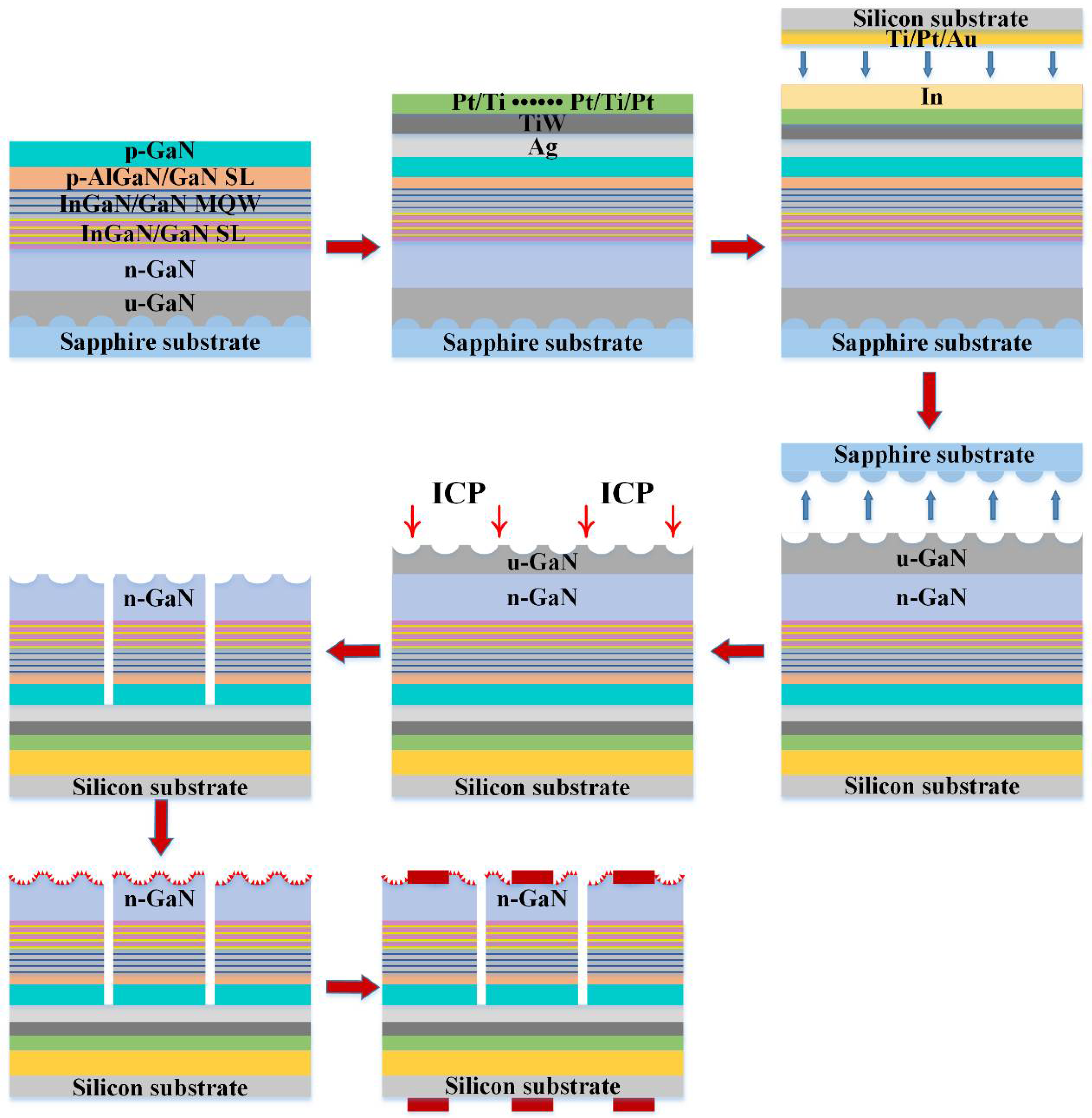
2. Materials and Methods

Figure 1 demonstrates a schematic illustration of the fabrication process for the vertical LEDs. A GaN-based LED epitaxial structure was grown on a 4 in. c-plane (0001)-patterned sapphire substrate (PSS) using metal–organic chemical vapor deposition (MOCVD). The LED epitaxial structure comprised a 25 nm-thick low-temperature GaN nucleation layer, 3.5 μm-thick undoped GaN buffer layer, a 2.5 μm-thick Si-doped n-GaN layer, a 3-period In0.05Ga0.95N (3 nm)/GaN (60 nm) superlattice I, a 5-period In0.05Ga0.95N (2 nm)/GaN (8 nm) superlattice II, 10-period In0.17Ga0.83N (3 nm)/GaN (10 nm) MQWs, a 40 nm-thick p-Al0.2Ga0.8N/GaN superlattice electron blocking layer, and a 120 nm-thick Mg-doped p-GaN layer. The GaN quantum barrier was grown at 870 °C, and then the temperature was adjusted to 780 °C to grow the InGaN quantum well. Finally, in order to activate Mg dopants in the p-GaN layer, the LED epilayers were annealed at 750 °C under N2 ambient.
After the epitaxial growth of the LED structure was completed, a 100 nm-thick Ag layer was deposited onto the p-GaN layer serving as a reflector by sputtering with a 5 × 10⁻⁵ Torr base pressure. In order to improve the thermal stability of Ag-based Ohmic contacts, an 80 nm-thick TiW alloy layer was deposited onto the Ag layer as a diffusion barrier by sputtering under a 5 × 10⁻⁵ Torr Ar pressure. Pt/Ti/Pt/Ti/Pt/Ti/Pt/Ti/Pt/Ti/Pt metallization layers were then deposited on the TiW alloy, followed by rapid thermal annealing at 600 °C to ameliorate the Ohmic contact between Ag and p-GaN. A 50 nm-thick Ti layer, 50 nm-thick Pt layer, and 1.2 μm-thick Au layer were deposited on the p-Si wafer, and a 2.5 μm-thick In layer was deposited on the LED wafer. Here, the Ti layer served as the Ohmic contact layer with the p-Si substrate, and the Pt layer served as the diffusion barrier. The Au and In were used as bonding metals. The LED wafer was then bonded to the p-Si substrate using thermal compression under 2000 kg pressure at 230 °C. The PSS was removed to expose the undoped GaN layer by LLO. In order to expose the surface of the n-GaN layer, the 3.5 μm-thick undoped GaN layer was etched using inductively coupled plasma (ICP) etching based on BCl3/Cl2 plasmas. The removal of the PSS and undoped GaN layer transferred the hemispherical dimples onto the surface of the n-GaN layer. ICP etching was performed to create channels in the GaN epilayers for die isolation (with an etching depth of about 3 μm), and a 1 mm × 1 mm square mesa-configuration was defined. To improve the LEE, integrated surface textures including micro-scale periodic hemispherical dimples and nano-scale random hexagonal pyramids were created on the surface of the n-GaN layer by potassium hydroxide (KOH) solution. Then, the SiO2 passivation layer was deposited using plasma-enhanced chemical vapor deposition (PECVD). Finally, Cr/Pt/Au multilayers for the n-electrode and Ti/Au multilayers for the p-electrode were deposited onto the backside of the p-Si wafer and the n-GaN surface, respectively.
Scanning electron microscopy (SEM) (Oxford Instruments, Oxford, UK) and transmission electron microscopy (TEM) (FEI, Hillsborough, OR, USA )combined with energy-dispersive X-ray (EDX) spectroscopy were used to analyze the surface morphology and structural features of the fabricated vertical LEDs. Raman measurement was performed using confocal Raman microscope (Renishaw, London, UK) to evaluate the stress state of InGaN/GaN MQWs using a confocal Raman microscope. PL measurement was employed at room temperature to characterize the emission property of InGaN/GaN MQWs using a 405 nm laser diode. Lumerical FDTD software was employed to investigate the LEE of the vertical LED with integrated surface textures. The light output power–current–voltage (L–I–V) characteristics of vertical LEDs with integrated surface textures were collected using an calibrated integrating sphere and a semiconductor parameter analyzer (Keysight B2901A) (Keysight, Santa Rosa, CA, USA).

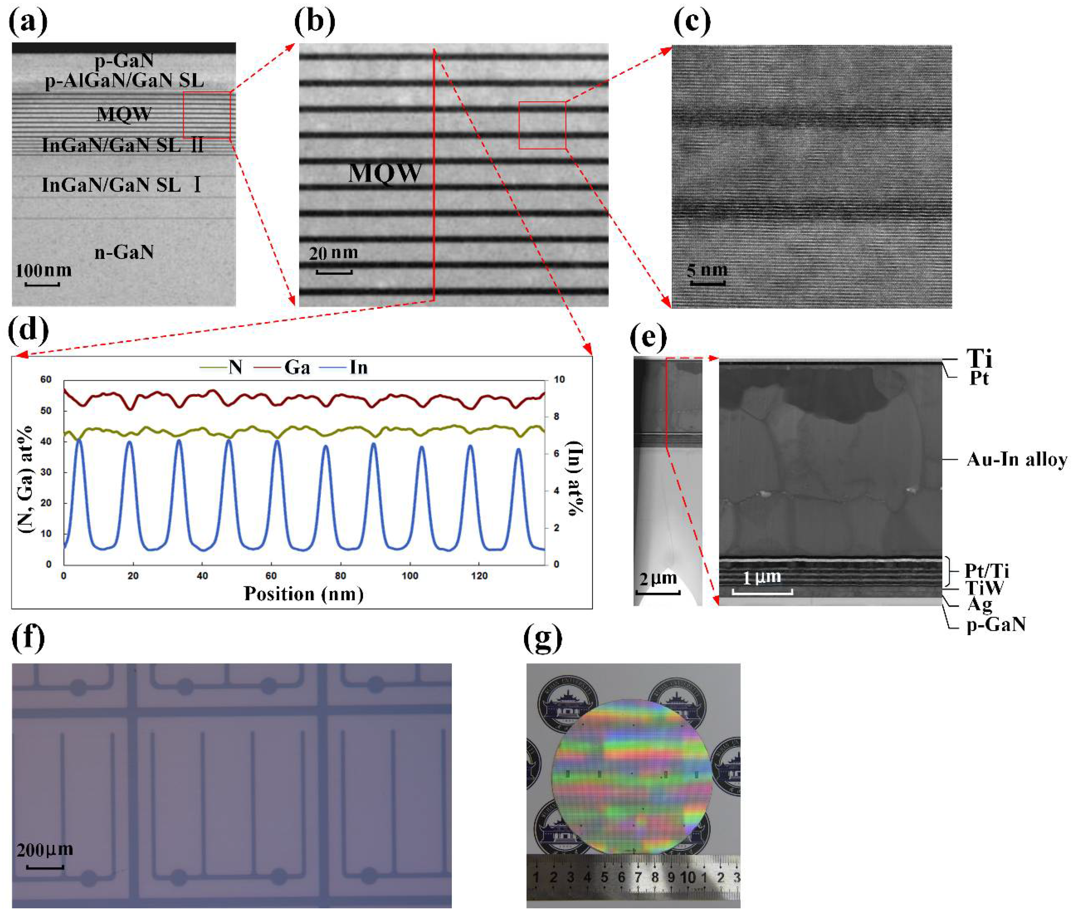
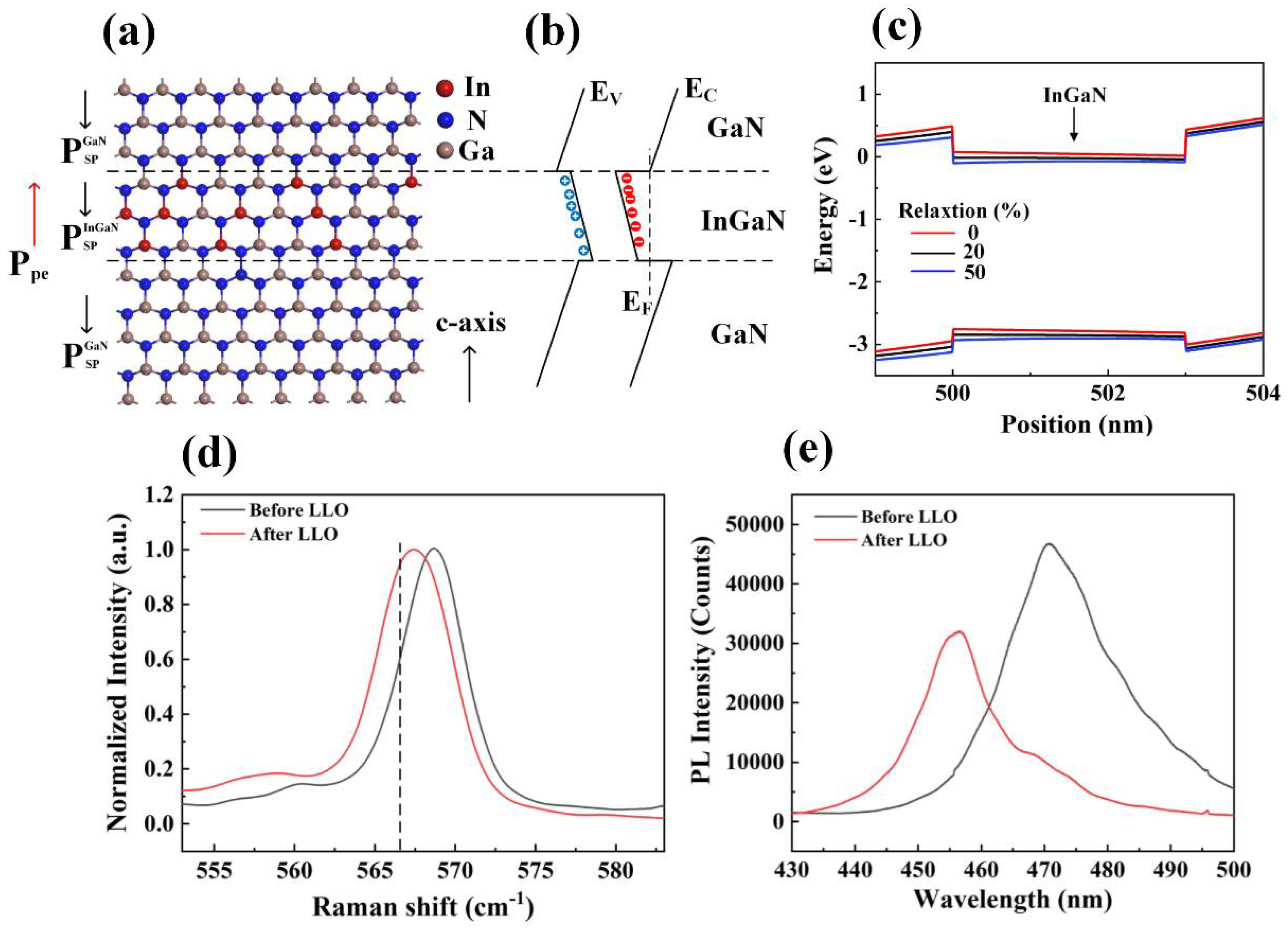
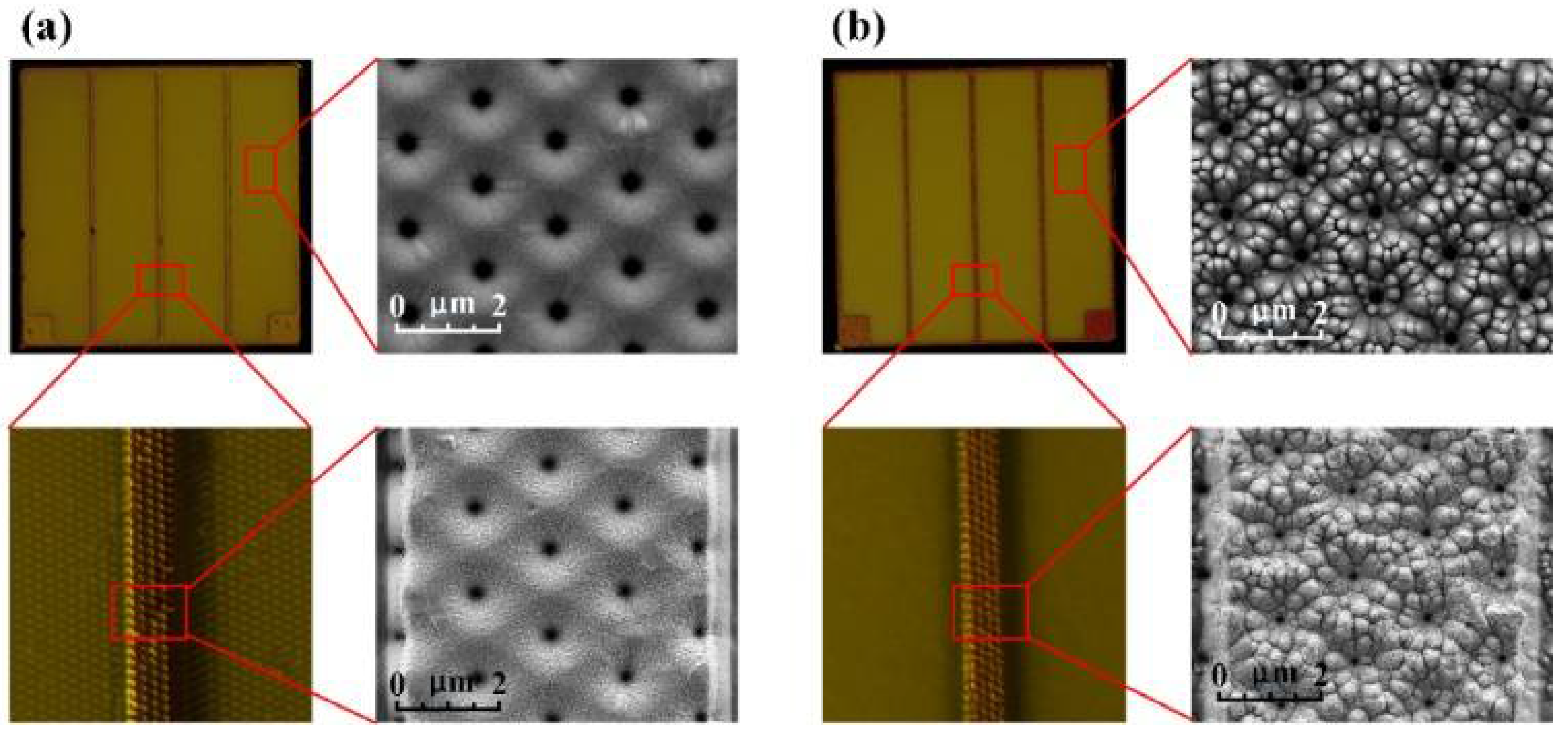
3. Results and Discussion

Figure 2a shows a cross-sectional TEM image of the LED epitaxial structure. In Figure 2a, the LED structure, including a n-GaN layer, 3-period In0.05Ga0.95N (3 nm)/GaN (60 nm) superlattice I, 5-period In0.05Ga0.95N (2 nm)/GaN (8 nm) superlattice II, 10-period In0.17Ga0.83N (3 nm)/GaN (10 nm) MQWs, p-Al0.2Ga0.8N/GaN superlattice, and a p-GaN capping layer, can be clearly observed. The InGaN/GaN superlattice I served mainly as a pre-strain layer for the reduction of the strain in the overlying active regions, while the InGaN/GaN superlattice II was an electron-injection layer, which can promote injected electrons tunneling and thermionic emission from the InGaN/GaN superlattice into the MQWs. The cross-sectional TEM image of the InGaN/GaN MQWs structure is demonstrated in Figure 2b. Clear stripes with a high contrast in the TEM image indicate abrupt heterointerfaces. Figure 2c shows a high-resolution cross-sectional TEM image of the InGaN/GaN MQW. Regular lattice arrays can be observed, suggesting a high-quality InGaN/GaN MQW structure. EDX analysis was performed to reveal the compositional variation along the InGaN/GaN MQW active regions vertically (the red line in Figure 2b). In Figure 2d, the result clearly confirms the spatial distributions of elemental Ga, In, and N in the different regions along the growth direction of the InGaN/GaN MQW structure. Figure 2e illustrates cross-sectional TEM images of Au-In bonding layers and the metallization scheme. The Ag film on the p-GaN is a metal reflector and the TiW acts as a diffusion barrier. The high-reflectivity Ag film decreased downward-absorbing light and improved the emission from the top facet and the side facets. The Pt/Ti films deposited on the Ag/TiW films protected them from environmental humidity. Au-In intermixing is observed during the wafer bonding process. The Ti/Pt layers on both sides of the bonding area prevented Au and In from further diffusing. Figure 2f,g show the optical microscope image and photograph of fabricated vertical LEDs on the Si substrate, respectively. The colorful patterns in Figure 2g are attributed to the thin-film interference effect.
Transferring the LED epilayers from the sapphire substrate onto the Si substrate can relieve the QCSE and further influence the emission property. Figure 3a shows the atomic structure model of the GaN/InGaN/GaN quantum well. Figure 3b shows the corresponding schematic illustration of the energy band structure. Due to its non-central symmetric crystal structure, there are two different types of polarizations existing in the GaN/InGaN/GaN quantum well: (i) The spontaneous polarization PspGaN and PspInGaN in GaN and InGaN layers, respectively; (ii) piezoelectric polarization in the InGaN layer (Ppe). The piezoelectric polarization results from the compressive stress in the InGaN layer owing to the large lattice mismatch between the (1) GaN epi-layer and sapphire substrate, as well as the (2) GaN barrier layer and InGaN active layer. The polarizations result in band tilting in the GaN layer and InGaN layer and the formation of a triangle-shaped potential well in the InGaN quantum well [39,40]. Thus, the electron and hole wave functions are separated. The adverse impacts red-shift the peak wavelength, decrease the spatial overlap between electron and hole wave functions, and reduce the localized carrier recombination efficiency. This phenomenon is known as the QCSE. The energy band structures of the GaN/InGaN/GaN single-quantum-well (SQW) structure under different compressive stress states are calculated using the SimuLED simulation software. The calculation is based on the 8 × 8 k · p method, universally referred to as the Kane model. The k · p method is a semiempirical method for solving the Schrödinger equation to obtain the band structure. Accompanied by the envelope function approximation, it provides a powerful tool for approximate calculation of the electron energies in low-dimensional structures such as quantum wells. The splitting of the heavy, light, and split-off branches of the valence bands in the center of the Brillouin zone is presumed to be unconnected to the built-in electric field. On this assumption, the profiles of the valence subbands are equal to each other and can be obtained from the solution of the coupled Poisson and transport equations. The conduction band can be further calculated by the effective mass approximation method [41,42,43,44]. Figure 3c shows the calculated energy band diagram of the SQW structure for different relaxation cases without applied bias voltage. Increasing the degree of relaxation, which means decreasing the compressive stress, flattens out the energy bands in the InGaN quantum well due to the reduction in piezoelectric polarization. With the degree of relaxation increasing, the calculated peak emission wavelength of the SQW structure blue-shifted. It is indicated that the relaxation of compressive stress can relieve the QCSE.
Removing the sapphire substrate using LLO can relax the compressive stress in the InGaN/GaN MQW caused by the lattice mismatch between the GaN epi-layer and the sapphire substrate. We use Raman spectroscopy to discover the stress states of the LED before and after LLO. Figure 3d shows normalized Raman spectra of the E2 (high) mode for the LED before and after LLO. The vertical dotted line shows the E2 (high) peak position for stress-free bulk GaN with the wavenumber of 566.65 cm–1. The Raman peaks before and after LLO are located at 568.5 and 567.4 cm–1, respectively. The Raman frequency will shift to the higher-frequency side of the stress-free position (blue shifts) because of the presence of residual compressive stress [45]. The stress in the GaN film can be calculated as follows:
σ = ω k
where ∆ω is the relative E2 (high) Raman peak shift, k is the Raman stress coefficient (4.2 cm−1/GPa) for the E2 (high) mode of GaN, and σ is the stress. From (1), the compressive stress of the LED before and after LLO is determined to be 458 and 182 MPa, respectively. Furthermore, the relaxation of compressive stress weakens the piezoelectric field. Thus, the band restores toward flat conditions and the overlap area of the electron and hole wave functions increases, alleviating the adverse impacts of QCSE. Hence, the peak emission wavelength blue-shifts and the localized carrier recombination efficiency increases after removing the sapphire substrate. The blue-shift in peak emission wavelength is verified by PL measurement. Figure 3e shows PL spectra (T = 300 K) of the LEDs before and after LLO measured using a 405 nm laser diode. As expected, due to the decrease in the compressive stress from 458 to 182 MPa, there is a shift in peak emission wavelength from 471 to 456 nm after LLO. However, the LED epilayers before LLO showed a higher PL intensity. The reasons were that the sapphire substrate could provide a gradual change in refractive index and contribute to LEE before LLO. Hence, the LED epilayers after LLO showed lower PL intensity although the QCSE was relieved. Thus, it was demonstrated that transferring LED epilayers from the sapphire substrate onto the Si substrate reduced the adverse impacts of the QCSE and blue-shifted the peak wavelength of the fabricated vertical LEDs.
After the PSS was lifted-off, hemispherical dimples were formed on the surface of the u-GaN layer [46]. The hemispherical dimples were transferred onto the surface of the n-GaN layer after removal of u-GaN because the etching depth was the same at different locations during the ICP etching process. After the LED wafer was dipped into the KOH solution to generate nano-scale random hexagonal pyramids on the corrugated n-GaN surface [47], integrated surface textures including micro-scale periodic hemispherical dimples and nano-scale random hexagonal pyramids were completed on the surface of the n-GaN layer. Figure 4a shows optical microscope images and SEM images of surface morphology of the n-GaN layer without KOH etching. We observed in Figure 4a that the patterned arrays of hemispherical dimples have been successfully transferred onto the surface of the n-GaN layer. Moreover, the surface does not have sub-micrometer-scale structures and is quite smooth. However, black areas in the middle of these semispherical dimples can be seen. The reason is that the center areas of these semispherical dimples are so deep that the real structural features in these areas cannot be clearly observed in the SEM. The corresponding optical microscope images and SEM images of surface morphology of the n-GaN layer with KOH etching are shown in Figure 4b. It is evident that numerous nano-scale cones are irregularly distributed on the whole surface after KOH etching. The integrated surface textures combined advantages of reducing the incident angles using the inclined surface of hemispherical dimples and scattering light using nano-scale structures.
We employed FDTD to investigate the light extraction ability of vertical LEDs with integrated surface textures. Figure 5a–c show schematic illustrations of the top surface morphologies of vertical LEDs with a flat surface, single micro-scale surface texture, and integrated surface textures, respectively. The simplified simulation models consisted of a 150 nm-thick p-GaN layer, 150 nm-thick MQWs, and 5 μm-thick u-GaN layer. In these simulation models, the N-polar surface was covered with pits, which were left by laser lift-off processing. The depth and top diameter of the pits in the simulation model were 1.7 and 2.7 μm. After etching by KOH solution, hexagonal pyramids generated on the N-polar surface. In these simulations, these hexagonal pyramids were replaced by cones with a height of 0.4 μm. The chip area used in these simulations was 20 × 20 μm2. The refractive index of p-GaN, MQWs, and n-GaN was set to 2.4, 2.5, and 2.4, respectively. These simulations of LEDs were embedded into a cuboid simulation domain with a perfectly matched layer (PML). Dipoles with a wavelength of 460 nm were arranged at intervals of 500 nm in the middle plane of the InGaN quantum-well. The monitors were stationed at a distance of 500 nm away from the simulation model to collect electric field components. Figure 5d–f show the normalized light-induced electric field intensity distributions on the top surface of the n-GaN layer for vertical LEDs with a flat surface, single micro-scale surface texture, and integrated surface textures, respectively. It is evident that a vertical LED with integrated surface textures has the largest electric field intensity on the top surface of the n-GaN layer, which means the strongest luminous intensity. The electric field intensity of LEDs without a surface texture is tinier than that of LEDs with a single micro-scale surface texture and integrated surface textures. The single micro-scale surface texture can reduce the incident angles using an inclined surface of hemispherical dimples. Hence, compared to that of a vertical LED with a flat surface, the LEE of a vertical LED with a single micro-scale surface texture increases by 116%. The integrated surface textures can further improve the LEE due to scattering light using nano-scale structures. The LEE of a vertical LED with integrated surface textures increased by 10.9% in a vertical LED compared to that of a vertical LED with a single micro-scale surface texture.
Figure 6 provides more evidence of the influence of integrated surface textures on the optical and electrical performance in a vertical LED. The current versus voltage and light output power versus current characteristics of the vertical LED with a single micro-scale surface texture and integrated surface textures are presented in Figure 6a,b, respectively. The vertical LED with integrated surface textures had higher light output power and lower forward voltage than the vertical LED with a single micro-scale surface texture at the same injection current. Under 350 mA injection current, the light output powers for the vertical LEDs with a single micro-scale surface texture and integrated surface textures were approximately 420.1 and 468.9 mW, respectively, accompanied by forward voltages of 2.90 and 2.88 V. One of the reasons for the slightly lower forward voltage of the vertical LED with integrated surface textures was probably better Ohmic contact between the n-GaN and the n-electrode. A standard KOH etching involves the oxidation of GaN and the subsequent dissolution of gallium oxide. Hence, surface gallium oxides can be removed and the preferential etching of Ga atoms may induce gallium vacancies at the surface in the etching process, which increased the surface barrier height by about 0.3 eV according to a previous report [48]. On the other hand, after KOH etching, integrated surface textures including micro-scale periodic hemispherical dimples and nano-scale random hexagonal pyramids were made on the n-GaN layer. The n-contact area was enlarged in the vertical LEDs with KOH etching (see Figure 4), which finally resulted in the reduced n-contact resistance [49]. The enhancement factor of the light output power was 11.4%, which is in agreement with the simulated LEE improvement provided equal internal quantum efficiency for both kinds of vertical LEDs. Figure 6c,d show the far-field radiation profiles of both kinds of vertical LEDs measured under a 350 mA injection current. Compared to vertical LEDs with a single micro-scale surface texture, vertical LEDs with integrated surface textures exhibited a more convergent emission pattern. Due to scattering light by nano-scale structures on the surface of the n-GaN layer, LEDs with integrated surface textures exhibited equal emission from the side facets and significantly enhanced emission from the top facet. Thus, vertical LEDs with integrated surface textures showed enhanced LEE.

4. Conclusions

In summary, we investigated the manufacturing process that contributed to optimizing the emission property for vertical LEDs on the p-type silicon substrate to understand the impacts of the manufacturing process on the optical performance. We revealed the effect of transferring LED epilayers from the sapphire substrate onto the Si substrate on the stress state and emission characteristics of the vertical LED. Moreover, we carried out an optical simulation to investigate the LEE of vertical LEDs with integrated surface textures. We found that, compared to the single micro-scale surface texture, integrated surface textures improved the LEE in a vertical LED due to the combined advantages of reducing the incident angles using the inclined surface of hemispherical dimples and scattering light using nano-scale structures. The simulation results show that the LEE of the vertical LED with integrated surface textures increases by 10.9% compared to that of the vertical LED with a single micro-scale surface texture. The experimental result showed good agreement with the numerical simulation. With the injection current of 350 mA, vertical LEDs with integrated surface textures manifested an excellent light output power of 468.9 mW. We conducted a systematic investigation of the optical properties of vertical LEDs, to reveal the impacts of the manufacturing process on their optical characteristics. We believe that this study can provide a deep understanding to design high-efficiency vertical LEDs on the p-Si substrate. What is more, the wafer bonding with the Si substrate, and the LLO and KOH etching techniques are applicable to vertical mini- and micro-LEDs. Our finding will also contribute to the pursuing of highly integrated optoelectronics on Si substrates.

Author Contributions

S.Z. originally conceived the idea. Y.L. (Yu Lei), B.T. and Z.W. wrote the manuscript. H.W., S.L. and J.M. carried out the simulations. S.Z. and Y.L. (Yingce Liu) carried out the fabrication and measurements. All authors have read and agreed to the published version of the manuscript.

Funding

This research was funded by the National Natural Science Foundation of China (Grant Nos. 51775387, 51675386) and Natural Science Foundation of Hubei Province (No. 2018CFA091).

Conflicts of Interest

The authors declare no conflict of interest.

References

  1. Tsao, J.Y.; Crawford, M.H.; Coltrin, M.E.; Fischer, A.J.; Koleske, D.D.; Subramania, G.S.; Wang, G.T.; Wierer, J.J.; Karlicek, R.F., Jr. Toward smart and ultra-efficient solid-state lighting. Adv. Opt. Mater. 2014, 2, 809–836. [Google Scholar] [CrossRef]
  2. Pust, P.; Schmidt, P.J.; Schnick, W. A revolution in lighting. Nat. Mater. 2015, 14, 454–458. [Google Scholar] [CrossRef]
  3. Lee, J.H.; Woo, K.Y.; Kim, K.H.; Kim, H.D.; Kim, T.G. ITO/Ag/ITO multilayer-based transparent conductive electrodes for ultraviolet light-emitting diodes. Opt. Lett. 2013, 38, 5055–5058. [Google Scholar] [CrossRef] [PubMed]
  4. Weisbuch, C.; Piccardo, M.; Martinelli, L.; Iveland, J.; Peretti, J.; Speck, J.S. The efficiency challenge of nitride light-emitting diodes for lighting. Phys. Status Solidi A Appl. Mat. 2015, 212, 899–913. [Google Scholar] [CrossRef]
  5. Chen, C.Y.; Liu, W.C. Light extraction enhancement of GaN-based light-emitting diodes with textured sidewalls and ICP-transferred nanohemispherical backside reflector. IEEE Trans. Electron Devices 2017, 64, 3672–3677. [Google Scholar] [CrossRef]
  6. Hu, H.; Tang, B.; Wan, H.; Sun, H.; Zhou, S.; Dai, J.; Chen, C.; Liu, S.; Guo, L.J. Boosted ultraviolet electroluminescence of InGaN/AlGaN quantum structures grown on high-index contrast patterned sapphire with silica array. Nano Energy 2020, 69, 104427. [Google Scholar] [CrossRef]
  7. Feng, Y.; Yang, X.; Zhang, Z.; Kang, D.; Zhang, J.; Liu, K.; Li, X.; Shen, J.; Liu, F.; Wang, T.; et al. Epitaxy of single-crystalline GaN film on CMOS-compatible Si (100) substrate buffered by graphene. Adv. Funct. Mater. 2019, 29, 1905056. [Google Scholar] [CrossRef]
  8. Ryou, J.; Yoder, P.D.; Liu, J.; Lochner, Z.; Kim, H.; Choi, S.; Kim, H.J.; Dupuis, R.D. Control of quantum-confined stark effect in InGaN-based quantum wells. IEEE J. Sel. Top. Quant. 2009, 15, 1080–1091. [Google Scholar] [CrossRef]
  9. Hu, H.; Zhou, S.; Wan, H.; Liu, X.; Li, N.; Xu, H. Effect of strain relaxation on performance of InGaN/GaN green LEDs grown on 4-inch sapphire substrate with sputtered AlN nucleation layer. Sci. Rep. 2019, 9, 3447. [Google Scholar] [CrossRef] [Green Version]
  10. Hu, H.; Zhou, S.; Liu, X.; Gao, Y.; Gui, C.; Gui, S. Effects of GaN/AlGaN/Sputtered AlN nucleation layers on performance of GaN-based ultraviolet light-emitting diodes. Sci. Rep. 2017, 7, 44627. [Google Scholar] [CrossRef]
  11. Liu, T.; Li, D.; Hu, H.; Huang, X.; Zhao, Z.; Sha, W.; Jiang, C.; Du, C.; Liu, M.; Pu, X.; et al. Piezo-phototronic effect in InGaN/GaN semi-floating micro-disk LED arrays. Nano Energy 2020, 67, 104218. [Google Scholar] [CrossRef]
  12. Tsai, S.C.; Lu, C.H.; Liu, C.P. Piezoelectric effect on compensation of the quantum-confined Stark effect in InGaN/GaN multiple quantum wells based green light-emitting diodes. Nano Energy 2016, 28, 373–379. [Google Scholar] [CrossRef]
  13. Jiang, J.; Wang, Q.; Wang, B.; Dong, J.; Li, Z.; Li, X.; Zi, Y.; Li, S.; Wang, X. Direct lift-off and the piezo-phototronic study of InGaN/GaN heterostructure membrane. Nano Energy 2019, 59, 545–552. [Google Scholar] [CrossRef]
  14. Liu, H.F.; Seng, H.L.; Teng, J.H.; Chua, S.J.; Chi, D.Z. Effects of lift-off and strain relaxation on optical properties of InGaN/GaN blue LED grown on 150mm diameter Si(111) substrate. J. Cryst. Growth 2014, 402, 155–160. [Google Scholar] [CrossRef]
  15. Guo, X.; Schubert, E.F. Current crowding in GaN/InGaN light emitting diodes on insulating substrates. J. Appl. Phys. 2001, 90, 4191–4195. [Google Scholar] [CrossRef]
  16. Horng, R.; Hsiao, H.; Chiang, C.; Wuu, D.; Tsai, Y.; Lin, H. Novel device design for high-power InGaN/sapphire LEDs using copper heat spreader with reflector. IEEE J. Sel. Top. Quant. 2009, 15, 1281–1286. [Google Scholar] [CrossRef]
  17. Zhou, S.; Liu, X.; Yan, H.; Chen, Z.; Liu, Y.; Liu, S. Highly efficient GaN-based high-power flip-chip light-emitting diodes. Opt. Express 2019, 27, A669–A692. [Google Scholar] [CrossRef] [PubMed]
  18. Yonkee, B.P.; Young, E.C.; DenBaars, S.P.; Nakamura, S.; Speck, J.S. Silver free III-nitride flip chip light-emitting-diode with wall plug efficiency over 70% utilizing a GaN tunnel junction. Appl. Phys. Lett. 2016, 109, 191104. [Google Scholar] [CrossRef]
  19. Tang, B.; Miao, J.; Liu, Y.; Wan, H.; Li, N.; Zhou, S.; Gui, C. Enhanced light extraction of flip-chip mini-LEDs with prism-structured sidewall. Nanomaterials 2019, 9, 319. [Google Scholar] [CrossRef] [PubMed] [Green Version]
  20. Lee, Y.L.; Cha, Y.J.; Oh, S.K.; Kim, T.K.; Hong, I.Y.; Kim, Y.S.; Kwak, J.S. Improvement of thermal stability of Ag-based reflector in GaN-based flip chip LEDs by electron-beam irradiation. Phys. Status Solidi A 2017, 214, 1600799. [Google Scholar] [CrossRef]
  21. Lee, G.J.; Hong, I.Y.; Kim, T.K.; Park, H.J.; Oh, S.K.; Cha, Y.J.; Park, M.J.; Choi, K.J.; Kwak, J.S. Design of ITO/SiO2/TiO2 distributed Bragg reflectors as a p-type electrode in GaN-based flip-chip light emitting diodes. Appl. Surf. Sci. 2019, 477, 220–225. [Google Scholar] [CrossRef]
  22. Kim, H.; Kim, K.; Choi, K.; Kim, H.; Song, J.; Cho, J.; Baik, K.H.; Sone, C.; Park, Y.; Seong, T. Design of high-efficiency GaN-based light emitting diodes with vertical injection geometry. Appl. Phys. Lett. 2007, 91, 023510. [Google Scholar] [CrossRef]
  23. Li, Y.; Wang, W.; Huang, L.; Zheng, Y.; Li, X.; Tang, X.; Xie, W.; Chen, X.; Li, G. High-performance vertical GaN-based near-ultraviolet light-emitting diodes on Si substrates. J. Mater. Chem. C 2018, 6, 11255–11260. [Google Scholar] [CrossRef]
  24. Zhou, S.; Xu, H.; Tang, B.; Liu, Y.; Wan, H.; Miao, J. High-power and reliable GaN-based vertical light-emitting diodes on 4-inch silicon substrate. Opt. Express 2019, 27, A1506–A1516. [Google Scholar] [CrossRef] [PubMed]
  25. Wong, W.S.; Sands, T. Damage-free separation of GaN thin films from sapphire substrates. Appl. Phys. Lett. 1998, 72, 599–601. [Google Scholar] [CrossRef]
  26. Kelly, M.K.; Vaudo, R.P.; Phanse, V.M.; Görgens, L.; Ambacher, O.; Stutzmann, M. Large free-standing GaN substrates by hydride vapor phase epitaxy and laser-induced liftoff. Jpn. J. Appl. Phys. 1999, 72, L217. [Google Scholar] [CrossRef]
  27. Tan, B.S.; Yuan, S.; Kang, X.J. Performance enhancement of InGaN light-emitting diodes by laser lift-off and transfer from sapphire to copper substrate. Appl. Phys. Lett. 2004, 84, 2757–2759. [Google Scholar] [CrossRef]
  28. Zhu, H.; Xi, J.; Liu, J.G. Fabrication and packaging of a vertical-structured UV LED device by laser lift-off of Sapphire. In Proceedings of the China International Forum on Solid State Lighting, Shenzhen, China, 21 December 2015. [Google Scholar]
  29. Cui, H.; Kim, W.J.; Park, S. Analysis for optimal size of current blocking layer in InGaN-based vertical LEDs. Semicond. Sci. Tech. 2019, 34, 105003. [Google Scholar] [CrossRef]
  30. Kang, J.H.; Ryu, J.H.; Kim, H.K.; Kim, H.Y.; Han, N.; Park, Y.J.; Uthirakumar, P.; Hong, C. Comparison of various surface textured layer in InGaN LEDs for high light extraction efficiency. Opt. Express 2011, 19, 3637–3646. [Google Scholar] [CrossRef]
  31. Kao, C.; Kuo, H.C.; Yeh, K.F.; Chu, J.T.; Peng, W.L.; Huang, H.W.; Lu, T.C.; Wang, S.C. Light–output enhancement of nano-roughened GaN laser lift-off light-emitting diodes formed by ICP dry etching. IEEE Photonics Technol. Lett. 2007, 19, 849–851. [Google Scholar] [CrossRef]
  32. Li, Z.; Cao, K.; Li, J.; Tang, Y.; Xu, L.; Ding, X.; Yu, B. Investigation of light-extraction mechanisms of multiscale patterned arrays with rough morphology for GaN-based thin-film LEDs. IEEE Access 2019, 7, 73890–73898. [Google Scholar] [CrossRef]
  33. Fujii, T.; Gao, Y.; Sharma, R.; Hu, E.L.; Denbaars, S.P.; Nakamura, S. Increase in the extraction efficiency of GaN based light-emitting diodes via surface roughening. Appl. Phys. Lett. 2004, 84, 855–857. [Google Scholar] [CrossRef]
  34. Zhao, P.; Zhao, H. Analysis of light extraction efficiency enhancement for thin-film-flip-chip InGaN quantum wells light-emitting diodes with GaN micro-domes. Opt. Express 2012, 20, A765–A776. [Google Scholar] [CrossRef] [PubMed]
  35. Jewell, J.; Simeonov, D.; Huang, S.C.; Hu, Y.L.; Nakamura, S.; Speck, J.; Weisbuch, C. Double embedded photonic crystals for extraction of guided light in light-emitting diodes. Appl. Phys. Lett. 2012, 100, 171105. [Google Scholar] [CrossRef]
  36. Ye, B.U.; Kim, B.J.; Song, Y.H.; Son, J.H.; Yu, H.K.; Kim, M.H.; Lee, J.L.; Baik, J.M. Enhancing light emission of nanostructured vertical light-emitting diodes by minimizing total internal reflection. Adv. Funct. Mater. 2012, 22, 632–639. [Google Scholar] [CrossRef]
  37. Xi, J.; Schubert, M.F.; Kim, J.K.; Schubert, E.F.; Chen, M.; Lin, S.; Liu, W.; Smart, J.A. Optical thin-film materials with low refractive index for broadband elimination of Fresnel reflection. Nat. Photonics 2007, 1, 176–179. [Google Scholar] [CrossRef]
  38. Oh, J.T.; Moon, Y.T.; Kang, D.S.; Park, C.K.; Han, J.W.; Jung, M.H.; Sung, Y.J.; Jeong, H.H.; Song, J.O.; Seong, T.Y. High efficiency ultraviolet GaN-based vertical light emitting diodes on 6-inch sapphire substrate using ex-situ sputtered AlN nucleation layer. Opt. Express 2018, 26, 5111–5117. [Google Scholar] [CrossRef]
  39. Jiang, C.; Jing, L.; Huang, X.; Liu, M.; Du, C.; Liu, T.; Pu, X.; Hu, W.; Wang, Z.L. Enhanced solar cell conversion efficiency of InGaN/GaN multiple quantum wells by piezo-phototronic effect. ACS Nano 2017, 11, 9405–9412. [Google Scholar] [CrossRef] [PubMed]
  40. Zhou, S.; Xu, H.; Hu, H.; Gui, C.; Liu, S. High quality GaN buffer layer by isoelectronic doping and its application to 365 nm InGaN/AlGaN ultraviolet light-emitting diodes. Appl. Surf. Sci. 2019, 471, 231–238. [Google Scholar] [CrossRef]
  41. Kane, E.O. Band structure of indium antimonide. J. Phys. Chem. Solids 1957, 1, 249–261. [Google Scholar] [CrossRef]
  42. Chuang, S.L.; Chang, C.S. k· p method for strained wurtzite semiconductors. Phys. Rev. B 1996, 54, 2491. [Google Scholar] [CrossRef] [PubMed]
  43. Wu, Y.; Lin, Y.; Huang, H.; Singh, J. Electronic and optical properties of InGaN quantum dot based light emitters for solid state lighting. J. Appl. Phys. 2009, 105, 013117. [Google Scholar] [CrossRef] [Green Version]
  44. Vinas, F.; Xu, H.Q.; Leijnse, M. Extracting band structure characteristics of GaSb/InAs core-shell nanowires from thermoelectric properties. Phys. Rev. B 2017, 95, 115420. [Google Scholar] [CrossRef] [Green Version]
  45. Park, B.; Kumar, R.S.; Moon, M.; Kim, M.; Kang, T.; Yang, W.; Kim, S. Comparison of stress states in GaN films grown on different substrates: Langasite, sapphire and silicon. J. Cryst. Growth 2015, 425, 149–153. [Google Scholar] [CrossRef]
  46. Chang, T.; Fang, H.; Liao, C.; Hsu, W.; Wu, Y.S. Laser lift-off mechanisms of GaN epi-Layer grown on pattern sapphire substrate. ECS J. Solid State Sci. 2014, 4, R20–R22. [Google Scholar] [CrossRef] [Green Version]
  47. Gao, Y.; Fujii, T.; Sharma, R.; Fujito, K.; Denbaars, S.P.; Nakamura, S.; Hu, E.L. Roughening hexagonal surface morphology on laser lift-off (LLO) N-face GaN with simple photo-enhanced chemical wet etching. Jpn. J. Appl. Phys. 2004, 43, L637. [Google Scholar] [CrossRef]
  48. Rickert, K.A.; Ellis, A.B.; Himpsel, F.J.; Sun, J.; Kuech, T.F. n-GaN surface treatments for metal contacts studied via x-ray photoemission spectroscopy. Appl. Phys. Lett. 2002, 80, 204–206. [Google Scholar] [CrossRef] [Green Version]
  49. Reddy, M.S.P.; Lee, J.H.; Jang, J.S. Electrical characteristics of TMAH-surface treated Ni/Au/Al2O3/GaN MIS schottky structures. Electron. Mater. Lett. 2014, 10, 411–416. [Google Scholar] [CrossRef]
Figure 1. Schematic illustration of the fabrication process of vertical LEDs.
Crystals 10 00621 g001
Figure 2. Cross-sectional TEM images of (a) the LED epitaxial structure and (b) the InGaN/GaN multiple quantum well (MQW). (c) High-resolution cross-sectional TEM images of the InGaN/GaN MQW. (d) Elemental concentration profile obtained from EDX line scanning along the red line. (e) Cross-sectional TEM image of the bonding layers. (f) Optical microscope image and (g) photograph of fabricated vertical LEDs on 4 inch Si wafer.
Crystals 10 00621 g002
Figure 3. (a) Cross-sectional TEM, (b) atomic structure model, and (c) schematic energy band structure of the GaN/InGaN/GaN quantum well. (d) Normalized Raman spectra of the E2 (high) mode for the LED epilayers before and after laser lift-off (LLO). (e) PL spectra (T = 300 K) of the LED epilayers before and after LLO.
Crystals 10 00621 g003
Figure 4. Optical microscope images and SEM images of surface morphology on n-GaN layer (a) without KOH etching and (b) with KOH etching.
Crystals 10 00621 g004
Figure 5. Schematic of the top surface morphologies of fabricated vertical LEDs with (a) flat surface, (b) single micro-scale surface texture, and (c) integrated surface textures. Normalized light-induced electric field intensity distributions on the top surface of n-GaN layer for vertical LEDs with (d) flat surface, (e) single micro-scale surface texture, and (f) integrated surface textures.
Crystals 10 00621 g005
Figure 6. (a) L–I and (b) I–V characteristics of the fabricated vertical LEDs with single micro-scale surface texture and integrated surface textures. Far-field radiation profiles of the fabricated vertical LEDs with (c) integrated surface textures and (d) single micro-scale surface texture.
Crystals 10 00621 g006

