Efficient Design Method for Plasmonic Filter for Tuning Spectral Selectivity


School of Electronics Engineering, College of IT engineering, Kyungpook National University, Daegu 41566, Korea
Crystals 2020, 10(6), 531; https://doi.org/10.3390/cryst10060531
Submission received: 12 May 2020
/
Revised: 14 June 2020
/
Accepted: 17 June 2020
/
Published: 23 June 2020
(This article belongs to the Special Issue Plasmonic Nanostructures)
Abstract
:Nano-structure-based color technologies have been reported as alternatives for conventional pigment- or dye-based color filters due to their simple design methods and durable characteristics. Since structure-based optical resonances accompany multiple resonance modes, spectral selectivity could be degraded. In this work, a simple and effective design of a plasmonic color filter that combines the plasmonic filter with one-dimensional photonic crystals. The introduced photonic crystal provides a photonic band gap, and it helps in suppressing the undesirable transmission peaks of the plasmonic color filter that originates from higher order resonance modes. Finally, the proposed design achieves high color purity. In addition, the simplicity of the design makes it both suitable for large-area fabrication and cost effective. This work is expected to provide a practical alternative to traditional color filters.
1. Introduction
With the rapid progress in nanofabrication, various phenomena occurring in sub-micron structures are being researched and reported, leading to advances in the application of nanostructures in various devices [1,2,3,4,5]. When nanostructures are formed in a metallic material, the collective oscillation of electrons at the metal–dielectric interface results in the generation of an electromagnetic (EM) wave. The power intensity of this EM field falls exponentially with increasing distance from the interface, and the wave propagates in a tangential direction to the surface. Therefore, this unique EM wave is referred to as the surface plasmon (SP). Generally, the SP appears in the spectral range from ultraviolet to infrared light with noble metals that have high conductivities. The SPs strongly interact with ambient EM resources within minuscule volumes. For example, the lights at the spectral range of resonance are trapped in the plasmonic structures. Consequently, the SPs are used by themselves or enhance other optical mechanisms such as absorption, scattering, emission, etc., which occur in the surroundings. From these points of view, plasmonic applications have been frequently explored for optical or photonic devices [6,7,8,9]. When SP resonance occurs in the visible range, plasmonic devices can be used as chromatic devices with selective spectral characteristics [10,11,12].
When light enters a thin metal film perforated by nanoholes, SPs are coupled with incident lights, resulting in considerable enhancement of light transmission through the aperture [13,14]. The transmittance exceeds the aperture ratio of the holes, and hence, this phenomenon is termed “extraordinary optical transmission” (EOT). The surface plasmon resonance (SPR) and EOT phenomena are affected by the refractive indices of the interface materials and by geometrical factors such as the thickness of the layers, the size and shape of the holes, and the periodicity. In particular, the periodicity of the pattern directly affects the EOT spectral range, which is related to the reciprocal of the dimension of the repeated arrangement.
With simple design factors by structural dimensions, nanohole arrays in metal films have been demonstrated for use in bandpass filters that show high transmission in a selective spectral range of EOT. In this regard, plasmonic color filters (PCFs) consisting of periodic metal hole arrays have been reported [15,16,17,18,19,20]. Most studies so far have been focused on the color-filtering functions with various structures. However, some issues have to be resolved to realize more practical applications of plasmonic filters. For example, the fabrication technologies should be suitable for mass production, and any imperfections in fabrication results in degraded spectral selectivity due to the broadening bandwidth. [15] Furthermore, multiple resonance modes originating from the periodic domain inevitably lead to multiple EOT peaks. Multiple transmission peaks and a broad bandwidth result in less saturated color, i.e., the color purity of the filter is reduced. Thus, the PCFs based on the metallic hole arrays are disadvantageous when seeking to use the metallic hole array structure as a color filter component in imaging devices.
In order to overcome the limitations of PCFs, a novel PCF combined with a one-dimensional photonic crystal (1DPhC) is proposed here. The repetition of the optical constant on the sub-micrometer scale results in a photonic band gap (PBG) where light modes cannot exist within the photonic crystal (PhC) structure. Based on this proposal, an optical design was realized to suppress undesired transmittance peaks in the PCF spectra by introducing a PBG. In the proposed structure, the integrated PBG suppressed undesirable transmission peaks and helped tune the bandwidth. Consequently, the color representability of the PCFs was improved.
2. Methods
In order to design transmittance curves with better color selectivity, a three-dimensional finite different time domain (FDTD) simulation (Lumerical Inc., Vancouver, Canada) was performed. The optical constants of each material are given in the experimental data. [21] Since the PCF has the periodicity of the hole arrays, the numerical calculation was performed with the unit cell. The symmetry and anti-symmetry boundary conditions were set in the x and y directions, respectively. A plane-wave light source with wavelength ranging from 200 nm to 1500 nm was used. The calculation was performed by using 401 values of wavelength to obtain the spectral response with the same frequency division (not the same wavelength division). The light source propagated along the z axis, and the perfect matching layer was set for the boundary condition in this direction.
3. Results and Discussion
3.1. Basic Design of the Red Plasmonic Filter
In a metallic hole array, the spectral position of transmittance peaks (λmax) corresponds to the SP resonance orders, following [13,22]
where P is the period of the array and εm and εd are the permittivity values of the metal and dielectric material, respectively. Optical resonance originates from the periodicity. The smallest periodic unit generates the fundamental resonance mode, and more modes appear corresponding to the periodic dimensions. The periodicity is calculated using (i,j) numbers in Equation (1) corresponding to the reciprocal vectors of the array. Among the multiple transmittance peaks, the highest transmittance occurs in the largest wavelength region corresponding to the first order of resonance [15]. If the pass band is to be positioned in red light, i.e., λmax(1,0) or λmax(0,1) lies between 600 nm and 700 nm, the second order peak (λmax(1,1)) appears within the range 420–500 nm, as expected from Equation (1). Therefore, the hole arrays for a red PCF inevitably introduce additional disturbances in the form of undesirable transmission peaks in the lower wavelength region. This leads to the deterioration of the color purity performance.
In this paper, a design method is proposed to suppress undesirable transmittance by combining PhCs with the conventional PCF structure. As atoms are periodically repeated in a solid crystal, PhCs consist of a structure in which optically different material compositions are regularly repeated. Such periodic structures make it possible to control the dispersion and velocity of light. One of the most interesting properties of PhCs is the PBG, which is a specific wavelength range in which the existence of optical modes is inhibited, similar to the electron energy band gap of crystal lattices. Based on the photonic band theory [23,24], the development of various device applications with PBGs is being actively researched [25,26]. If different dielectric constants are repeated in a certain direction, light is scattered at the interfaces of layers, resulting in destructive interference in the direction of the repeated change of dielectric constants. Therefore, light of specific energy levels cannot propagate in that direction.
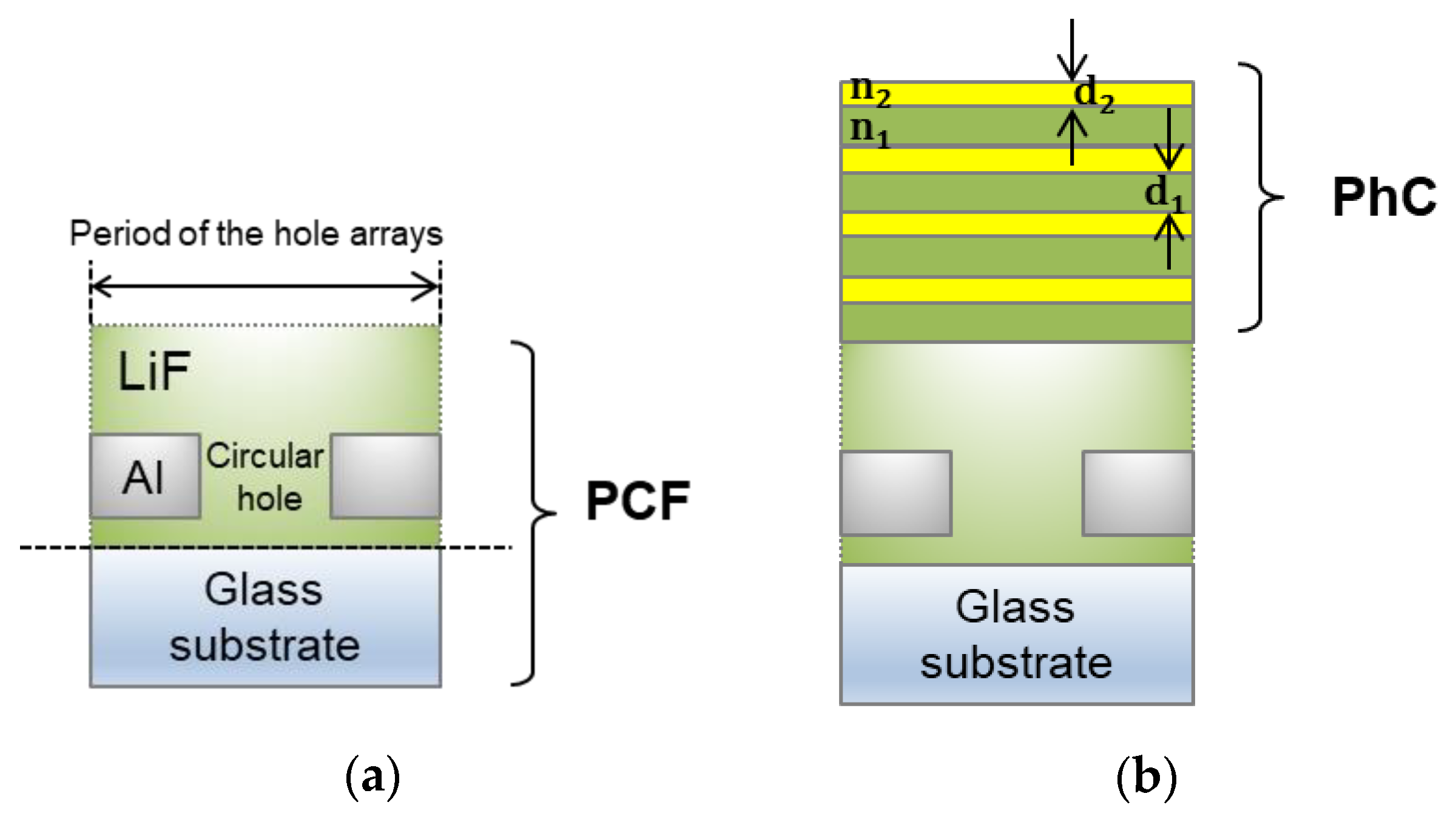
In the proposed structure, the spectral range of the PBG is adjusted at the wavelength of the second order peak of a red PCF. Figure 1 shows the schematic diagram of the PCF structure for filtering red light. The reference PCF structure shown in Figure 1a has hole arrays in a 150-nm-thick aluminum (Al) film on a glass substrate. The diameter of the holes is 240 nm, and the period of the square array is 370 nm. Lithium fluoride (LiF) layers cover the top and bottom of the Al film; the thickness of the top and bottom LiF layers are 150 nm and 50 nm, respectively. These thicknesses are selected to obtain effectively the same SP modes [27].
The proposed filter is shown in Figure 1b. One-dimensional (1D) periodicity is the simplest structure adopted to form a PBG; it allows us to simplify the modified structure in terms of both design and fabrication. Two different dielectric materials are stacked alternatively on the top of the reference PCF, forming a 1DPhC structure. The periodic interval in the direction orthogonal to the surface of the structure generates a PBG during normal transmission. In a previous experimental study, the reference structure exhibited optimized transmittance with the quasi-plane surface [15]. Thus, the surface of each layer of 1DPhC can be assumed to be flat.
3.2. Design Photonic Bandgap in the Stop Band of the Plasmonic Filter
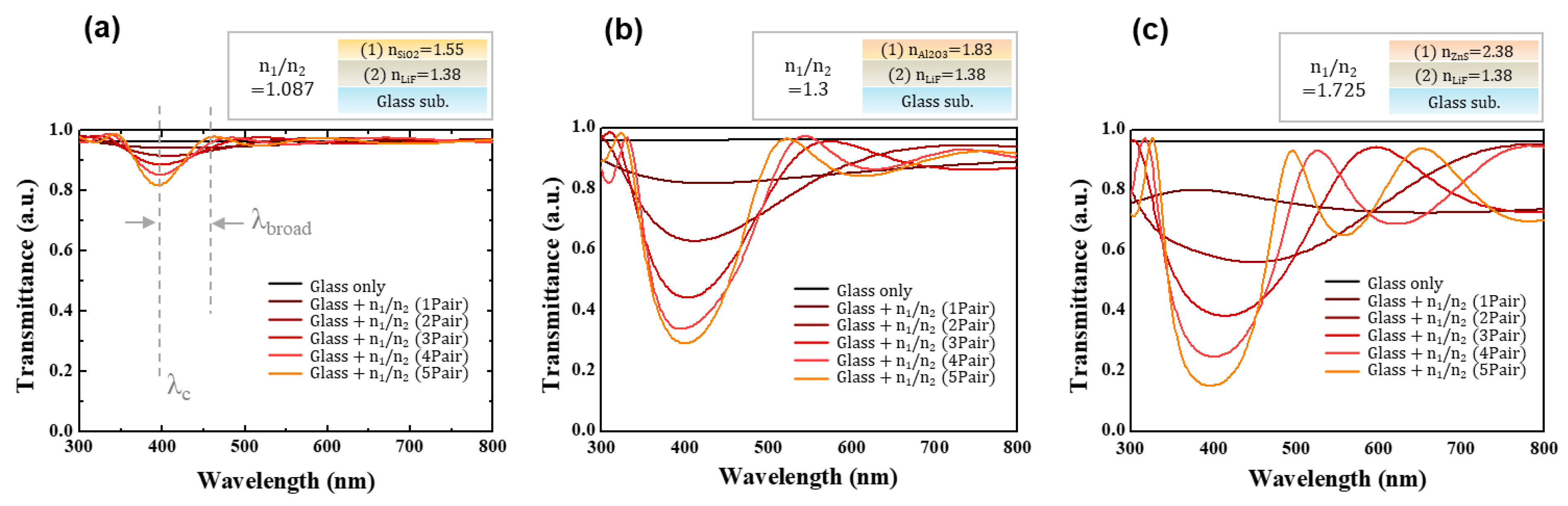
First, the spectral characteristics of 1DPhCs with a finite number of multilayers were examined. The optical properties of 1DPhCs were engineered to provide high reflection and low transmission at PBG with the central wavelength of 400 nm. Since infinite repetition is not practically possible, the constructed PBG is expected to have a low quality factor (Q-factor). Thus, the transmittance curve of the PhC may result in a wide and shallow valley. In addition, the finite number of interfaces within the multilayers is the main cause of the ripples beyond the PBG range in the transmission spectrum. These ripples originate from the constructive and destructive interferences between various reflection modes. Smaller numbers of interfaces result in larger amplitude and wider shape of the ripples. The transmittance spectrum of the optimized PhC to be integrated on a red PCF should have a valley in the cutoff band (approximately 400–600 nm) and a peak only in the red wavelength range. In addition, the shape of the spectral valley should not be symmetrical about the center wavelength of PBG and should be wider on the longer wavelength side. Considering these requirements, the designed PhCs have a PBG with a central wavelength of 400 nm, which is less than the range of λmax(1,1) of the red PCF.
The transmission spectra of 1DPhCs were calculated for various combinations of dielectric materials according to the number of stacked pairs. For all cases, two different dielectric materials were laid in sequence on the glass substrate, and the PhCs contain LiF along with the following three dielectric materials: (a) silicon dioxide (SiO2); (b) aluminium oxide (Al2O3); and (c) zinc sulfide (ZnS). The thickness of each material in the PhC is designed according to the following equation [28]:
where d and nd are the thickness and refractive index of each material, respectively, and λPBG is the central wavelength of the PBG (400 nm in this study). The refractive index values are not constant in the spectral range of interest. For defining d, the real value of nd at 400 nm was used. The refractive index value and thickness of each material layer were as follows: (i) nLiF = 1.38, dLiF = 72.5 nm; (ii) nSiO2 = 1.55, dSiO2 = 64.5 nm; (iii) nAl2O3 = 1.83, dAl2O3 = 54.6 nm; and (iv) nZnS = 2.38, dZnS = 42.0 nm.
Figure 2 shows the transmittance spectra of each 1DPhC laid on the glass substrate. Since a finite set of two materials were stacked in each 1DPhC, a perfect bandgap at 400 nm could not be realized. The strength of the PBG effect resulted in either a transmission or reflection spectrum around 400 nm. Since the PBG was used to restrict the second order peak (λmax(1,1)) of the red PCF, the effects of PBG were interpreted by reducing the transmittance at λPBG. As shown in Figure 2, as the number of layers increased, the disallowed band developed more readily. In all cases, at least two pairs of materials were required to form a distinct valley around 400 nm. The valley deepened as the number of layers increased. In addition, as the number of layers increased, the valley became narrower, and the central wavelength of the valley showed a blue-shift.
For the LiF/SiO2 composition shown in Figure 2a, the minimum transmittance of two pairs was 0.914 at 406.7 nm. The transmittance of the spectral valley reduced by 0.097 (~10.6%) and reached 0.817 at 394.5 nm, showing a spectral shift of 12.2 nm to the shorter range. The valley is not exactly symmetric with respect to the minimum transmittance position. Further, the filtering performance is measurable only in the visible range. Hence, in order to examine the broadness of the transmittance valley, the spectral distance (λbroad) was confirmed from the wavelength of minimum transmittance near 400 nm to the first maximum transmittance on the right side. In the case of the LiF/SiO2 structure, the use of five pairs resulted in a narrower transmittance valley with 67.2 nm λbroad, while for the structure with two pairs, λbroad was 193.5 nm.
The larger the contrast ratio of the refractive indexes between two materials of the PhC (n1/n2), the more distinct the PBG; consequently, lower transmittance was observed around 400 nm. In contrast, in the case with five pairs, the minimum transmittance was 0.817 for the smallest contrast ratio (1.087 in Figure 2a) and 0.152 for the case with the largest contrast ratio (1.725 in Figure 2c). In addition, when the contrast ratio of the index values was large, the valley became narrower and deeper and more distinct corresponding to the use of more layers. In Figure 2b, for LiF/Al2O3 with n1/n2 of 1.3, the minimum transmittance of the two pair structure was 0.62 (412.2 nm), and it reduced to 0.292 (at 401.4 nm) for five pairs. For the LiF/ZnS structure shown in Figure 2c, the minimum transmittance showed a reduction in 72.9%, decreasing from 0.561 to 0.152 when the number of stacked layers increased from two pairs to five pairs. In addition, the valley became narrower, resulting in a change in λbroad from 120.6 nm to 97.8 nm under identical conditions.
Meanwhile, ripples were observed in the longer wavelength range. The ripples become clearer and their amplitude increases as the ratio n1/n2 increases or as more layers are stacked. The ripples are the result of the interferences of the reflected light modes from various interfaces. In other words, in the dielectric layer that forms the interfaces with the other materials (of different optical constants), multiple reflections occur between the two interfaces. These light modes have a regular optical path difference, resulting in constructive and destructive interference, and finally showing repeating maxima and minima in the spectral range. This phenomenon is well known and forms the basis of the Fabry–Perot interferometer (FPI). The PhC structure has multiple interfaces, and hence, various reflected modes generate complex interference effects.
On the other hand, the entire PhC can be considered as an FPI that has the interfaces with the glass substrate at the bottom and with the air on the other side. The spectral distance between multiple transmittance peaks (λFSR: free spectral range) is affected by the thickness of the FPI structure. It is calculated as [29]
where λ0 is the central wavelength of the transmittance peak; n, the average refractive index value; and d, the thickness of the FPI. The greater the number of stacks in PhC, the thicker the FPI, the smaller is the value of λFSR, and thus, more ripples are created within the wavelength range of interest. A larger average refractive index of FPI yields similar results. Therefore, the case of the structure with five pairs of LiF/ZnS layers resulted in the most distinct and frequently positioned ripples. Thus, the transmittance curves could be designed. In order to improve the spectral selectivity of the filter by using the PhC, the transmittance of the PhC should be high in the pass band and low in the other wavelength bands. For example, three or five pairs of LiF/ZnS layers is acceptable over the four-pair structure, which has a weak transmittance valley in the red wavelength range.
Next, let us consider the optimized design of the red PCF combined with a PhC (PhC-PCF). As shown in Figure 2, the use of more layers resulted in low transmittance, close to zero, at the PBG. However, infinite repetition of layers is not practically possible. Further, multiple additionally deposited layers are inefficient in terms of mass production, even though a one-dimensionally repeated stack is very simple and can be achieved without any complex pattering techniques. In this regard, the proposed PhC-PCF was designed to reduce the number of the layers of PhC.
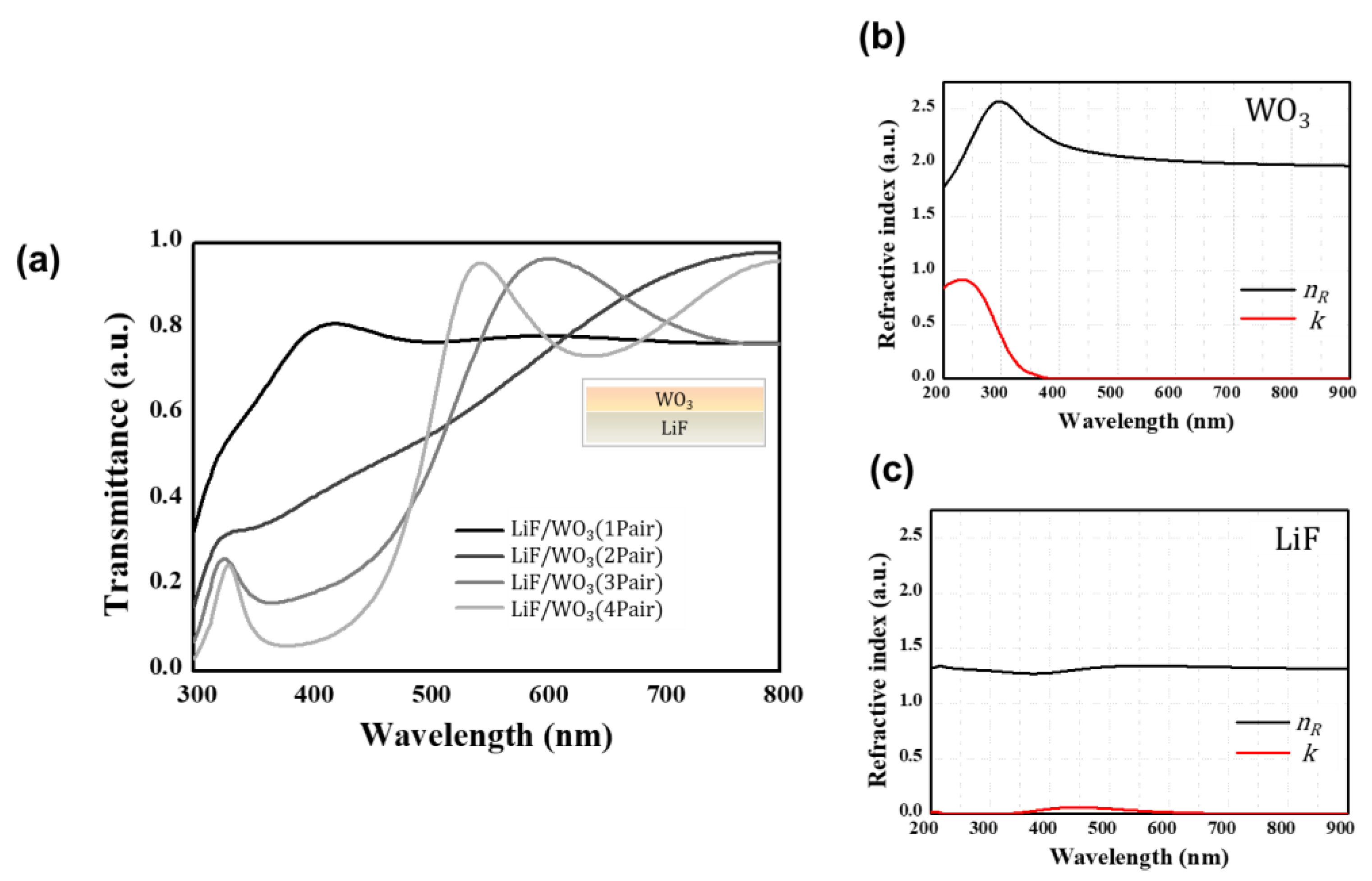
Previously, the fabrication process of the reference PCFs in Figure 1a has been reported, which adopted the laser interference lithography (LIL) method [15]. First, the coherent laser lights produce periodic patterns. Then, the photoresistive thin film is exposed by the interference patterns, and the following steps are the same as conventional photolithography, which is widely used in the industry. Compared to the conventional nano-patterning technologies such as electron-beam lithography and focused ion beam methods, the process revealed the possibility of the PCF fabrication in large area within short time. For comprising the proposed PhC-PCF in Figure 1b, the PhC consisted of LiF and tungsten trioxide (WO3) layers. Both materials can be deposited by thermal evaporation in the same chamber. The in situ process is also advantageous for large-area fabrication and cost effectiveness. The refractive indices were experimentally obtained from the thermally evaporated thin film. The LiF and WO3 layers were 72.5 nm and 45 nm thick, respectively, when calculated using (2) to achieve λPBG = 400 nm. The contrast ratio of the refractive indices of these two materials is 1.61, which is quite similar to that in the case shown in Figure 2c.
Figure 3a shows the transmission spectra of pairs of LiF and WO3 thin layers in free space. The glass substrate shows low loss in light transmission and does not have any spectral dependency. Therefore, the spectral responses of the multilayer stacks regardless of the presence or absence of the glass substrate are quite similar. The transmittance curves of the multi-layered stack were calculated to interpret only the effects of PhC by excluding the PCF in the final structure shown in Figure 1b. Similar to the results shown in Figure 2, more pairs of LiF/WO3 layers resulted in a more distinct valley, and thus showed low transmittance around 400 nm. Here, the structures composed of at least three pairs of LiF/WO3 layers revealed a distinct valley in the 400 nm wavelength band and ripples in the longer wavelength range. The transmittance at 400 nm was 0.181 for the three-pair structure, and it was reduced to 0.066 for the four-pair structure.
The refractive indices of LiF and WO3 are shown in Figure 3b,c, respectively. The measured optical constant of the WO3 thin film showed resonance characteristics near 230 nm. The maximum value of the imaginary part of the refractive index (k) was 0.918 at 233 nm. It reduced gradually, and k became zero at wavelengths greater than 390 nm. The imaginary part contributes to optical absorption, and the absorption resonance can be interpreted by the Lorentz oscillation model. The real part of the susceptibility, centered on the resonance frequency, oscillates between the positive and negative values, resulting in the curvature of the real part of the refractive index (nR), as shown in Figure 3b. At wavelengths longer than the resonance wavelength, the maximum value of nR for WO3 was 2.57 at 298 nm. This value is much larger than that in the wavelength range from 400 nm (2.18) to 700 nm (1.99).
The observed resonance characteristics resulted in high transmission loss in the 300 nm wavelength range and consequently led to the formation of an asymmetrical valley at λPBG. The broadness of the valley (λbroad) was defined as that from the target PBG band (λPBG, 400 nm) to the first peak position on the right side. The values of λbroad were 202.0 nm and 143.5 nm for the three-pair and four-pair structures, respectively. As the number of the stacked layers increased, the transmittance curve of the 4-pair structure showed ripples, and a shallow valley appeared between 500 nm and 700 nm. The minimum transmittance in this wavelength range was 0.736 at 641 nm. For LiF/WO3, the three-pair structure, with the smallest number of layers, was the most suitable for enhancing the spectral selectivity of the PCF.
3.3. Adjusting Spectral Response of PCF Using 1D-Phcs
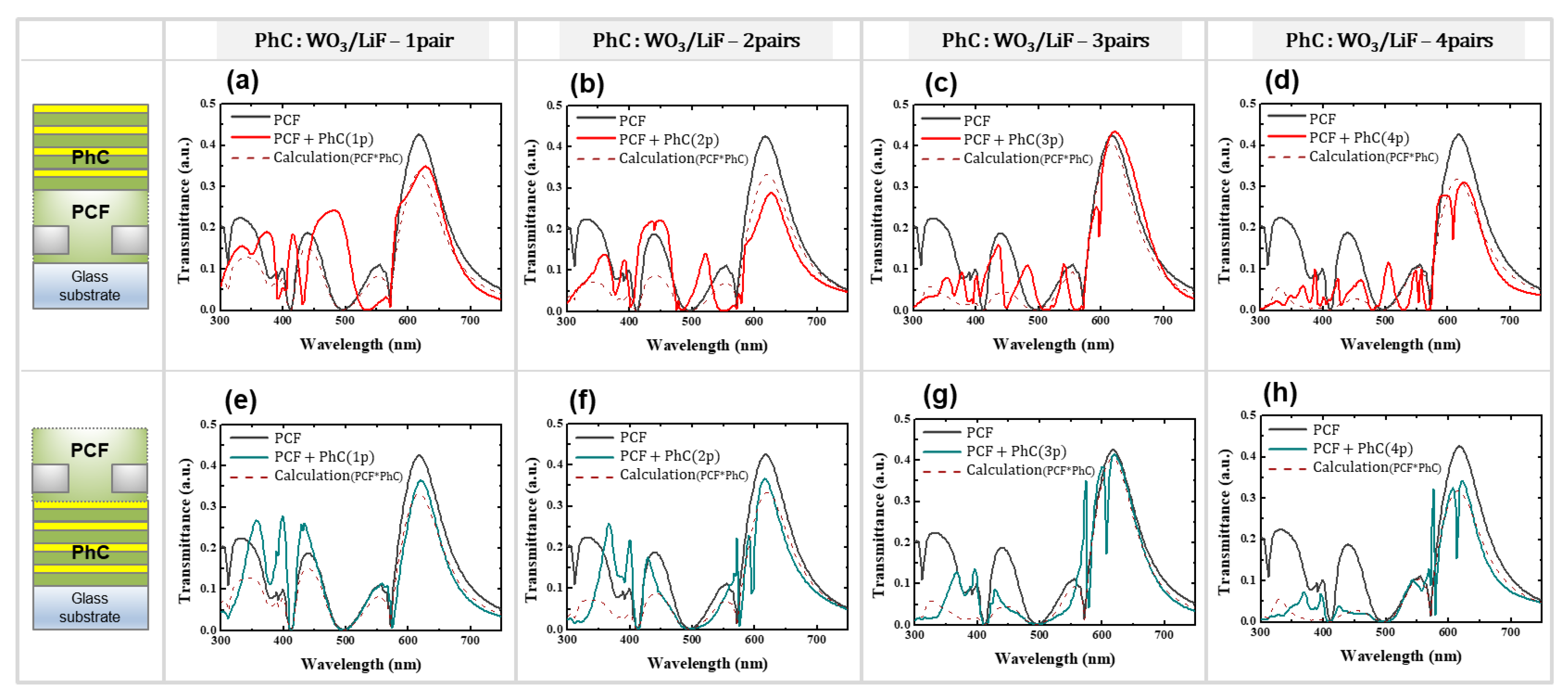
To investigate the effect of PBG on the whole structure, the transmittance spectra of the PhC-PCFs were simulated. The simulation was performed to determine the most efficient way to handle PhC. The proposed structures have different orders of the position of the PhC: (i) glass/PCF/PhD and (ii) glass/PhC/PCF. Figure 4 summarizes the change in the spectral response when the PhC was used in the reference PCF structure. Figure 4a–d shows the results for glass/PCF/PhC structures, and Figure 4e–h shows the transmission spectra for structures containing PhC, i.e., for glass/PhC/PCF structures. The transmittance curves of the PhC-PCFs were compared to the optical response of the reference PCF (Figure 2a). In all graphs, dashed lines show the transmission calculated as a simple product of the transmittance of PhC in Figure 3a and that of the reference PCF.
As expected, the use of three pairs of LiF/WO3 layers helps suppress the transmission in the spectral range from 400 nm to 600 nm while maintaining transmission in the range of λ1 of the PCF. These trends can be observed in Figure 4c,g. The spectra of the PhC-PCF structure resulted in a transmittance peak at λ1 similar to that of the PCF. Although transmittance in the wavelength range below 600 nm decreased, more peaks appeared randomly. For all cases shown in Figure 4, the spectral shapes at λ1 well corresponded to that of the calculated shapes. However, for two curves in the shorter wavelength range, the difference between the calculation and the simulated data was quite large.
In the first case, (i), the peak value of the PhC-PCF structure at λ1 was smaller than that of the calculated value for structures with two pairs or four pairs of PhC (Figure 4b,d). On the other hand, the peak value is larger than the calculated value in Figure 4a,c. The most similar case between the calculated and simulated results is shown in Figure 4c—the case of three pairs of layers, which results in a peak shift of 7 nm and a difference of 6.6% in peak transmittance (0.407 at 616 nm for the simulation and 0.434 at 623 nm for the calculation). In the short wavelength range below 600 nm, the simulation results show additional sharp peaks. These ripples affect the peak at λ1 when the PhC is composed of more than three pairs of layers.
In case (ii), in which PhC is inserted between the glass substrate and the metallic hole arrays, the transmittance peak of the PhC-PCF at λ1 is larger than the calculated value. In this case, the additional ripples appeared even in the peak at λ1 with more than two pairs of PhC layers. The greatest similarity between the simulation and calculation is shown in Figure 4e, i.e., for the one-pair structure. The peak transmittance was 0.332 at 618 nm in the simulation and 0.365 at 620 nm as per the calculation. The difference between the simulated and calculated values is smaller than that in case (i).
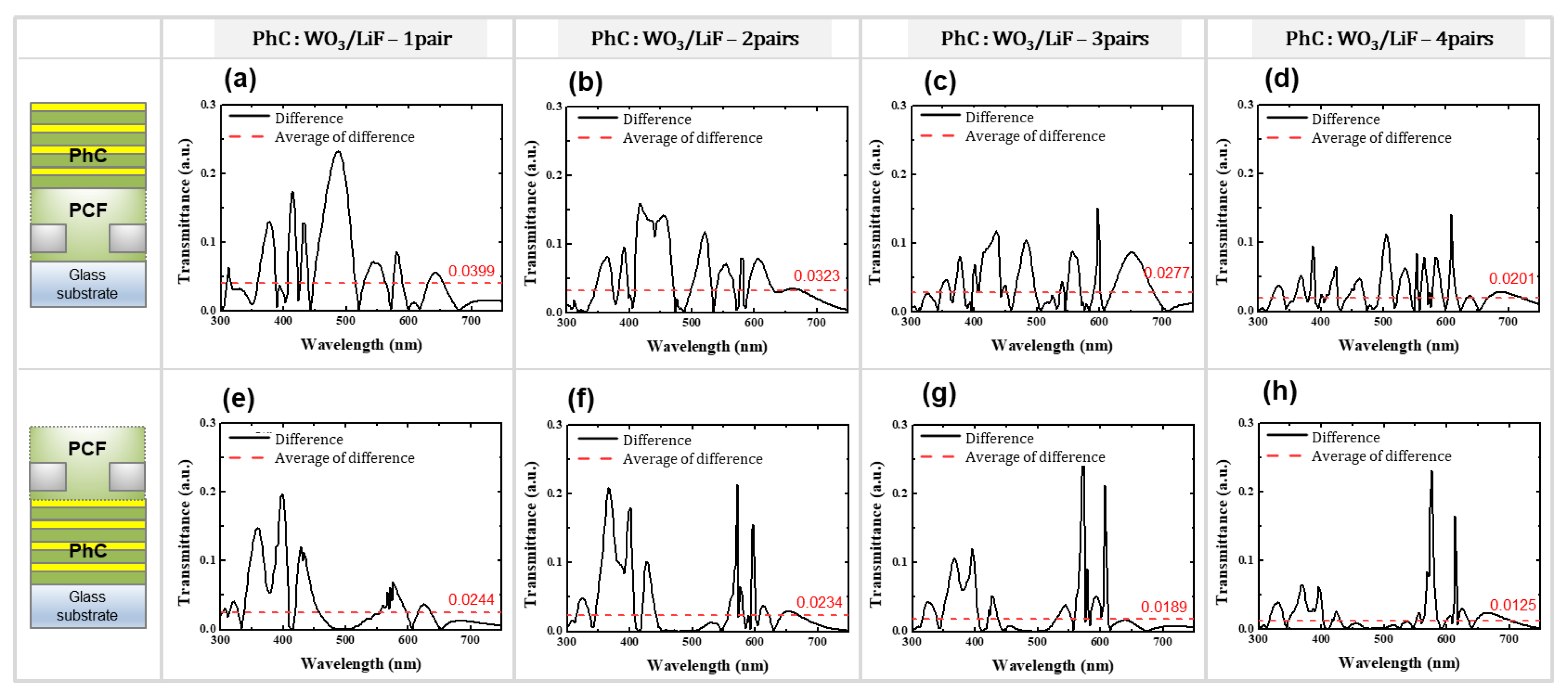
In order to analyze the effect of PhC quantitatively, the difference between the simulated and calculated values according to the wavelength (Figure 5) were considered. The results for glass/PCF/PhC structures are shown in Figure 5a–d, and those for glass/PhC/PCF structures are shown in Figure 5e–h, according to the numbers of PhCs. The numbers in each graph represent the average values of the differences in the spectral range from 300 nm to 800 nm. The difference between the calculated and simulated results decreased as the number of layers of the PhC increased. Additionally, a comparison of the structures with the same PhC composition (for example, Figure 5b,f or Figure 5d,h) showed that additional PhC layers between the substrate and the PCF led to a reduction in the difference between the calculated and simulated results. The smallest average difference was 0.0201 in case (i) and 0.0125 in case (ii); the value for case (ii) is 1.6 times smaller than that for case (i).
The calculated spectra indicate a situation in which the optical functions of the PCF and the PhC are separated. The effect of the additional dielectric layers on enhancing SPR and other possible optical effects through the multiple interfaces were not considered. In this regard, the smaller average difference between the calculations and the simulated results implies that the two components work more independently. In addition, the effect of PhC is more dominant than that of the complex optical interactions between the light modes generated from the additionally introduced interfaces. A comparison of the calculated and simulated results shows that the PhC inserted in the medium of the PCF provides more PBG-like effects.
Meanwhile, in terms of PBG formation with a finite numbers of layers, case (ii), i.e., glass/PhC/PCF structures, may be more effective. In these structures, light first undergoes PBG and then encounters the metallic surface of the PCF before passing through the PCF. Although the metal film enhances SP modes and scattering at the holes, the dominantly film-like shape results in high reflection. Thus, the round trip between the glass substrate and the metal film results in a larger number of effective layers for PhCs. In this regard, PhCs can be used for adjusting the transmission spectra of the reference PCF. The handling of PhCs in types of case (ii) is a more efficient way to control the spectra of the PCF with less layers. Compared to case (i), the optical response of case (ii) was closer to the expected value by considering only the PCF and PhCs and not any complex phenomena. In this work, the spectral response of the three pairs of LiF/WO3 layer was suitable to adjust the main transmittance peak as well as to suppress the minor transmittance peaks of the red PCF.
Although the reflective type of color filters is widely applicable in e-paper and various sensor devices, most imaging devices such as displays and CMOS image sensors adapt the transmissive type of color filters. These industrial devices demonstrate the full color image by the combination of red, green, and blue sub-pixels. From this perspective, the main goal of this study is to design a transmissive color filter as simple as possible. Since PBG from PhCs also provide the spectral selectivity, it can be also possible to form color filters by utilize PhC by itself. PBG works as an obstacle for light passing through the PhC structure; thus, it provides the band stop range in the spectra in terms of transmission. Referring the spectral selectivity of PBG in Figure 2, it could be possible to realize cyan, yellow, and magenta as primary colors for the transmissive type of color filter. It can also be inferred that high reflectivity with spectral selectivity is obtained by PBG (a reflective type of color filter) and, in this case, realize red, green, and blue primary color. Photonic crystals can also be used to make transmissive filters with a high wavelength selectivity. In this case, two-dimensional or three-dimensional photonic crystals are often used [30,31].
In addition, the plasmonic filters could expand the use of color filter device due to active controllability [32,33]. The SP resonance condition is affected by both the refractive index values of materials and the dimensions of the structure. By reversing the refractive index change from dielectric materials such as phase change materials (from thermal energy), liquid crystals with electrical, and optical anisotropy, there is a polymerization state in the conducting polymers. Especially, the plasmonic structure consists of a novel metal with high conductivity, and the SP structure provides active spectral controllability without any additional component when using the electrical tuning method. In these regards, the simple guideline to design the transmissive plasmonic color filter with high selectivity will help to enlarge the use of nano-optic phenomena in practical applications.
4. Conclusions
In this work, a novel plasmonic color filter that works in conjunction with a 1D PhC structure was proposed. In the finitely stacked multilayer, which does not form a complete PBG, the spectral valley is observed in the PBG band (central wavelength: 400 nm), and ripples are observed around the spectral range from 500 nm to 700 nm. The PBG band suppresses the undesirable transmittance peaks of the PCF. In addition, the shallow ripples resulting from the PBG band help adjust the spectral shape of the PCF in the pass-band range. Thus, the proposed structure provides a method to tune and optimize the transmittance curves of PCFs. When the PhC structure was positioned between the SP-enhanced hole arrays and a glass substrate, the light traveled twice the length of the PhC structure because of the highly reflective metallic boundary. Therefore, the glass/PhC/PCF structure resulted in PBG more effectively with fewer layers compared to the glass/PCF/PhC structure. Further, the complexity of the structure design was also less in the case of the glass/PhC/PCF structure. Thus, the proposed structure achieves good color purity and has the potential to serve as an alternative for pigment- or dye-based conventional color filters.
Funding
This research was supported by the Kyungpook National University Research Fund, 2017.
Conflicts of Interest
The author declares no conflict of interest.
References
- Lal, S.; Link, S.; Halas, N.J. Nano-optics from sensing to waveguiding. Nat. Photoniscs 2007, 1, 641–648. [Google Scholar] [CrossRef]
- Ozbay, E. Plasmonics: Merging photonics and electronics at nanoscale dimensions. Science 2006, 311, 189–193. [Google Scholar] [CrossRef] [PubMed]
- Moon, Y.G.; Do, Y.S.; Lee, M.H.; Hwang, B.Y.; Jeong, D.J.; Ju, B.K.; Choi, K.C. Plasmonic chromatic electrode with low resistivity. Sci. Rep. 2017, 7, 15206. [Google Scholar] [CrossRef] [PubMed]
- Han, J.H.; Kim, D.; Lee, T.W.; Jeon, Y.; Lee, H.S.; Choi, K.C. Color purifying optical nanothin film for three primary colors in optoelectronics. ACS Photonics 2018, 5, 3322–3330. [Google Scholar] [CrossRef]
- Kim, J.Y.; Lee, S.; Do, Y.S. Optimized Structure for a Moisture-Sensitive Colorimetric Sensor Utilizing Photonic Crystals Based on a Metal–Organic Framework. IEEE Access 2019, 7, 85483–85491. [Google Scholar] [CrossRef]
- Tan, S.J.; Zhang, L.; Zhu, D.; Goh, X.M.; Wang, Y.M.; Kumar, K.; Qiu, C.W.; Yang, J.K.W. Plasmonic color palettes for photorealistic printing with aluminum nanostructures. Nano Lett. 2014, 14, 4023–4029. [Google Scholar] [CrossRef]
- Do, Y.S.; Choi, K.C. Poly-periodic hole arrays for angle-invariant plasmonic filters. Opt. Lett. 2015, 40, 3873–3876. [Google Scholar] [CrossRef]
- Mansuripur, M.; Zakharian, A.R.; Lesuffleur, A.; Oh, S.H.; Jones, R.J.; Lindquist, N.C.; Im, H.; Kobyakov, A.; Moloney, J.V. Plasmonic Nano-Structures for Optical Data Storage. Opt. Express 2009, 17, 14001–14014. [Google Scholar] [CrossRef]
- Pang, L.; Hwang, G.M.; Slutsky, B.; Fainman, Y. Spectral Sensitivity of Two-Dimensional Nanohole Array Surface Plasmon Polariton Resonance Sensor. Appl. Phys. Lett. 2007, 91, 123112. [Google Scholar] [CrossRef]
- Song, M.; Wang, D.; Peana, S.; Choudhury, S.; Nyga, P.; Kudyshev, Z.A.; Yu, H.; Boltasseva, A.; Shalaev, V.M.; Kildishev, A.V. Colors with plasmonic nanostructures: A full-spectrum review. Appl. Phys. Rev. 2019, 6, 041308. [Google Scholar] [CrossRef] [Green Version]
- Fleischman, D.; Fountaine, K.T.; Bukowsky, C.R.; Tagliabue, G.; Sweatlock, L.A.; Atwater, H.A. High Spectral Resolution Plasmonic Color Filters with Subwavelength Dimensions. ACS Photonics 2019, 6, 332–338. [Google Scholar] [CrossRef] [Green Version]
- Miyamichi, A.; Ono, A.; Kamehama, H.; Kagawa, K.; Yasutomi, K.; Kawahito, S. Multi-band plasmonic color filters for visible-to-near-infrared image sensors. Opt. Express 2018, 26, 25178–25187. [Google Scholar] [CrossRef]
- Ebbesen, T.W.; Lezec, H.J.; Ghaemi, H.F.; Thio, T.; Wolff, P.A. Extraordinary Optical Transmission through Sub-Wavelength Hole Arrays. Nature 1998, 391, 667–669. [Google Scholar] [CrossRef]
- Ghaemi, H.F.; Thio, T.; Grupp, D.E.; Ebbesen, T.W.; Lezec, H.J. Surface plasmons enhance optical transmission through subwavelength holes. Phys Rev. B 1998, 58, 6779–6782. [Google Scholar] [CrossRef] [Green Version]
- Do, Y.S.; Park, J.H.; Hwang, B.Y.; Lee, S.M.; Ju, B.K.; Choi, K.C. Plasmonic color filter and its fabrication method for large area applications. Adv. Opt. Mater. 2013, 1, 133–138. [Google Scholar] [CrossRef]
- Do, Y.S.; Choi, K.C. Matching surface plasmon modes in symmetry-broken structures for nanohole-based plasmonic color filter. IEEE Photonics Technol. Lett. 2013, 25, 2454–2457. [Google Scholar] [CrossRef]
- Yokogawa, S.; Burgos, S.P.; Atwater, H.A. Plasmonic color filters for CMOS image sensor applications. Nano Lett. 2012, 12, 4349–4354. [Google Scholar] [CrossRef]
- Do, Y.S. A highly reproducible fabrication process for large-area plasmonic filters for optical applications. IEEE Access 2018, 6, 68961–68967. [Google Scholar] [CrossRef]
- Cho, H.J.; Do, Y.S. Plasmonic Color Filter with Robustness against Cross Talk for Compact Imaging Applications. Curr. Opt. Photonics 2020, 4, 16–22. [Google Scholar]
- Chen, Q.; Cumming, D.R.S. High transmission and low color cross-talk plasmonic color filters using triangular-lattice hole arrays in aluminum films. Opt. Express 2010, 18, 14056–14062. [Google Scholar] [CrossRef]
- Palik, E.D. Handbook of Optical Constants of Solids; Academic Press: San Diego, CA, USA, 1998. [Google Scholar]
- Genet, C.; Van Exter, M.P.; Woerdman, J.P. Fano-type interpretation of red shifts and red tails in hole array transmission spectra. Opt. Commun. 2003, 225, 331–336. [Google Scholar] [CrossRef] [Green Version]
- Yablonovitch, E. Inhibited Spontaneous Emission in Solid-State Physics and Electronics. Phys. Rev. Lett. 1987, 58, 2059–2062. [Google Scholar] [CrossRef] [PubMed] [Green Version]
- Ohtaka, K. Energy-Band of Photons and Low-Energy Photon Diffraction. Phys. Rev. B 1979, 19, 5057–5067. [Google Scholar] [CrossRef]
- Bowden, C.M.; Dowling, J.P.; Everitt, H.O. Development and Applications of Materials Exhibiting Photonic Band Gaps Introduction. J. Opt. Soc. Am. B-Opt. Phys. 1993, 10, 280–282. [Google Scholar] [CrossRef]
- Scherer, A.; Doll, T.; Yablonovitch, E.; Everitt, H.O.; Higgins, J.A. Guest Editorial: Electromagnetic Crystal Structures, Design, Synthesis, and Applications. J. Lightwave Technol 1999, 17, 1928–1930. [Google Scholar] [CrossRef] [Green Version]
- Do, Y.C.; Choi, K.C. Quantitative analysis of enhancing extraordinary optical transmission affected by dielectric environment. J. Opt. 2014, 16, 065005. [Google Scholar] [CrossRef]
- Bendickson, J.M.; Dowling, J.P.; Scalora, M. Analytic expressions for the electromagnetic mode density infinite, one-dimensional, photonic band-gap structures. Phys. Rev. E 1996, 53, 4107–4121. [Google Scholar] [CrossRef] [PubMed]
- Hecht, E. Optics, 3rd ed.; Addison-Wesley: New York, MA, USA, 1998. [Google Scholar]
- Choi, H.J.; Choi, S.; Yoo, Y.E.; Jeon, E.C.; Yi, Y.; Park, S.; Choi, D.S.; Kim, H. Transmission-type photonic crystal structures for color filters. Opt. Express 2013, 21, 18317–18324. [Google Scholar] [CrossRef]
- Singh, B.R.; Sawal, S.; Sinha, R.K. Photonic crystal-based RGB primary colour optical filter. J. Mod. Opt. 2016, 63, 1391–1396. [Google Scholar] [CrossRef]
- Xiong, K.; Tordera, D.; Jonsson, M.P.; Dahlin, A.B. Active control of plasmonic colors: Emerging display technologies. Rep. Prog. Phys. 2019, 82, 024501. [Google Scholar] [CrossRef] [Green Version]
- Gugole, M.; Olsson, O.; Xiong, K.; Blake, J.C.; Montero Amenedo, J.; Bayrak Pehlivan, I.; Niklasson, G.A.; Dahlin, A. High-Contrast Switching of Plasmonic Structural Colors: Inorganic vs. Organic Electrochromism. ACS Photonics 2020. [Google Scholar] [CrossRef]
Figure 1.
Schematics of the structure of plasmonic color filters (PCFs). (a) The reference PCF, (b) the proposed PCF in which a one-dimensional photonic crystal (PhC) is integrated onto the top of the reference PCF.
Figure 1.
Schematics of the structure of plasmonic color filters (PCFs). (a) The reference PCF, (b) the proposed PCF in which a one-dimensional photonic crystal (PhC) is integrated onto the top of the reference PCF.

Figure 2.
Effect of dielectric one-dimensional photonic crystals (1DPhCs). Transmission spectra of 1DPhCs formed on the glass substrate and containing different dielectric materials: (a) LiF and silicon oxide (SiO2); (b) LiF and aluminum oxide (Al2O3); and (c) LiF and zinc sulfide (ZnS). All graphs show the spectral changes according to the numbers of layers.

Figure 3.
(a) Transmission spectra of multiple layers composed of Lithium fluoride (LiF) and tungsten trioxide (WO3) in free space. The measured refractive indices of the thermally evaporated thin films—(b) WO3 and (c) LiF.
Figure 3.
(a) Transmission spectra of multiple layers composed of Lithium fluoride (LiF) and tungsten trioxide (WO3) in free space. The measured refractive indices of the thermally evaporated thin films—(b) WO3 and (c) LiF.

Figure 4.
Transmission spectra of PCFs combined with 1D-PhCs (WO3 and LiF). (a–d) show the results for glass/PCF/PhC structures, and (e–h) show the results for glass/PhC/PCF structures. In all graphs, the dashed lines represent the product of PhC effects (in Figure 3) and the transmittance of the reference PCF.

Figure 5.
Difference between the calculated and simulated spectra of the PhC-PCF in Figure 4. (a–d) show the results for glass/PCF/PhC structures, and (e–h) show the results for glass/PhC/PCF structures. The dashed line represents the average values of the differences in each case.
Figure 5.
Difference between the calculated and simulated spectra of the PhC-PCF in Figure 4. (a–d) show the results for glass/PCF/PhC structures, and (e–h) show the results for glass/PhC/PCF structures. The dashed line represents the average values of the differences in each case.

© 2020 by the author. Licensee MDPI, Basel, Switzerland. This article is an open access article distributed under the terms and conditions of the Creative Commons Attribution (CC BY) license (http://creativecommons.org/licenses/by/4.0/).
Share and Cite
MDPI and ACS Style
Do, Y.S. Efficient Design Method for Plasmonic Filter for Tuning Spectral Selectivity. Crystals 2020, 10, 531. https://doi.org/10.3390/cryst10060531
AMA Style
Do YS. Efficient Design Method for Plasmonic Filter for Tuning Spectral Selectivity. Crystals. 2020; 10(6):531. https://doi.org/10.3390/cryst10060531
Chicago/Turabian StyleDo, Yun Seon. 2020. "Efficient Design Method for Plasmonic Filter for Tuning Spectral Selectivity" Crystals 10, no. 6: 531. https://doi.org/10.3390/cryst10060531
Note that from the first issue of 2016, this journal uses article numbers instead of page numbers. See further details here.