Low Gate Lag Normally-Off p-GaN/AlGaN/GaN High Electron Mobility Transistor with Zirconium Gate Metal

 ,
, 
Abstract
:1. Introduction
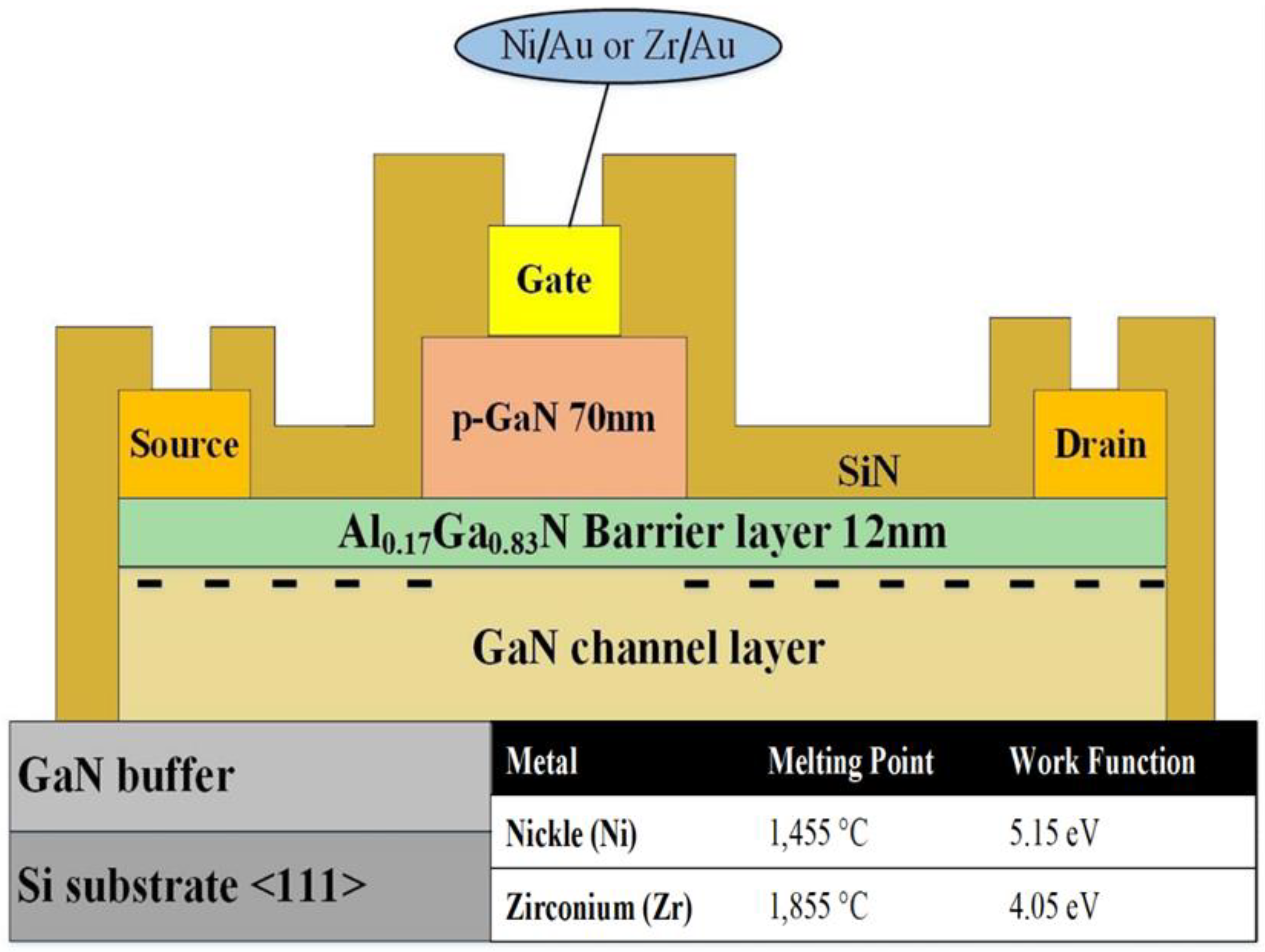
2. Device Structure
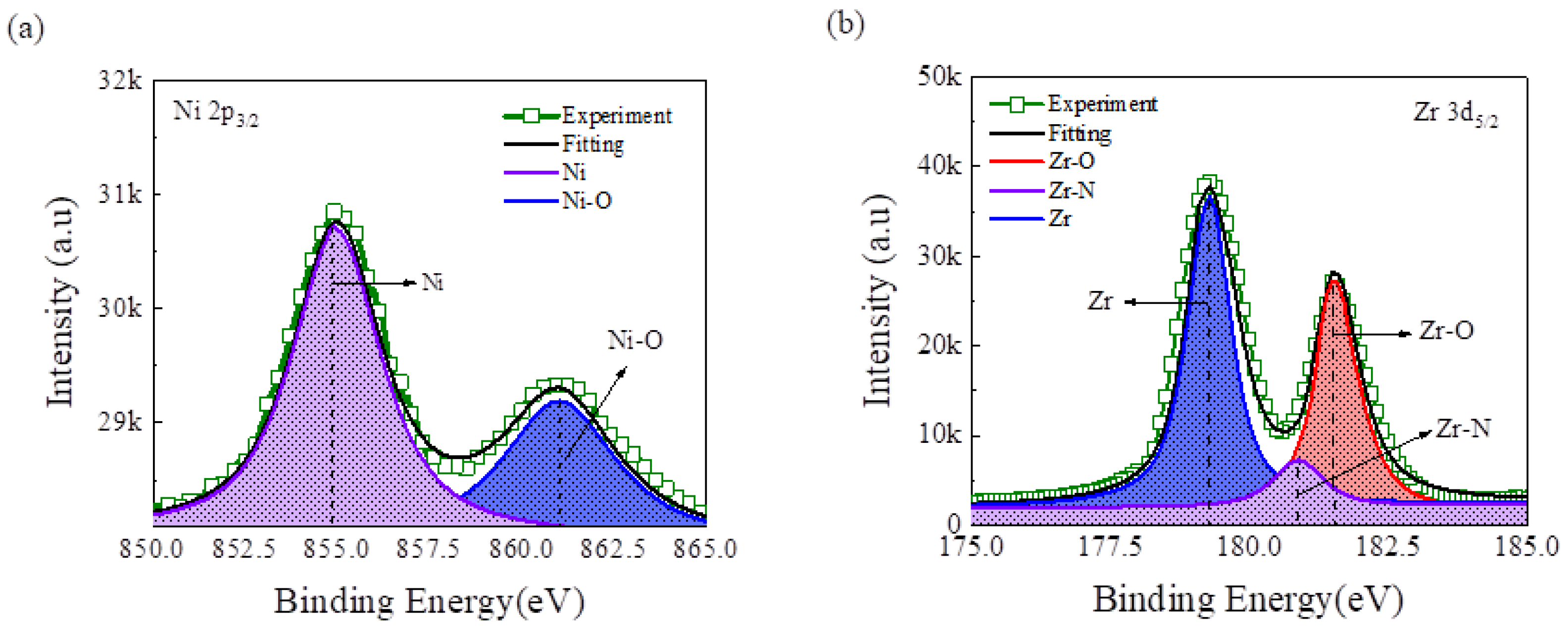
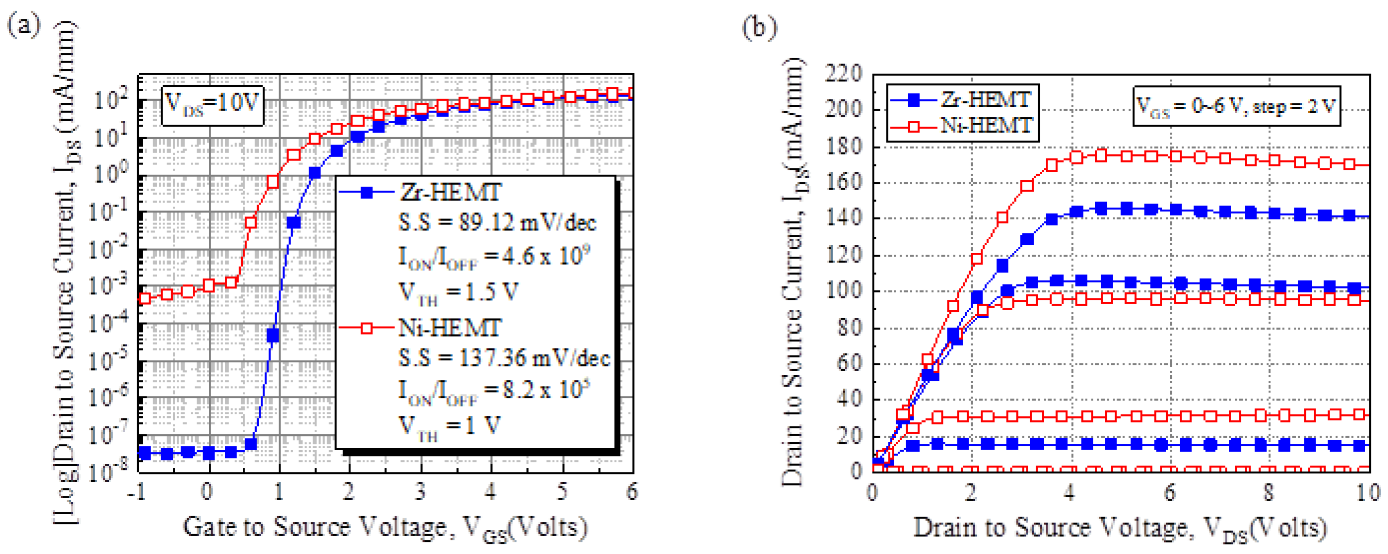
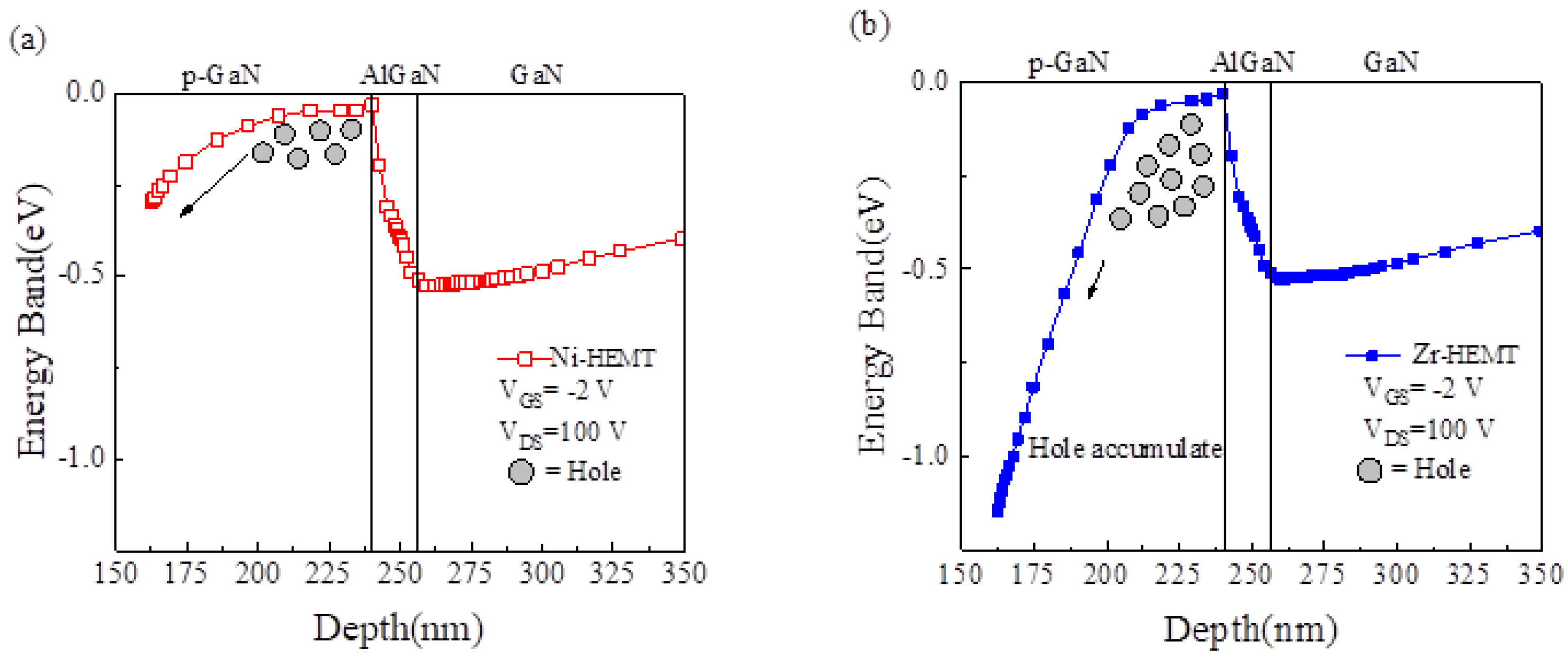
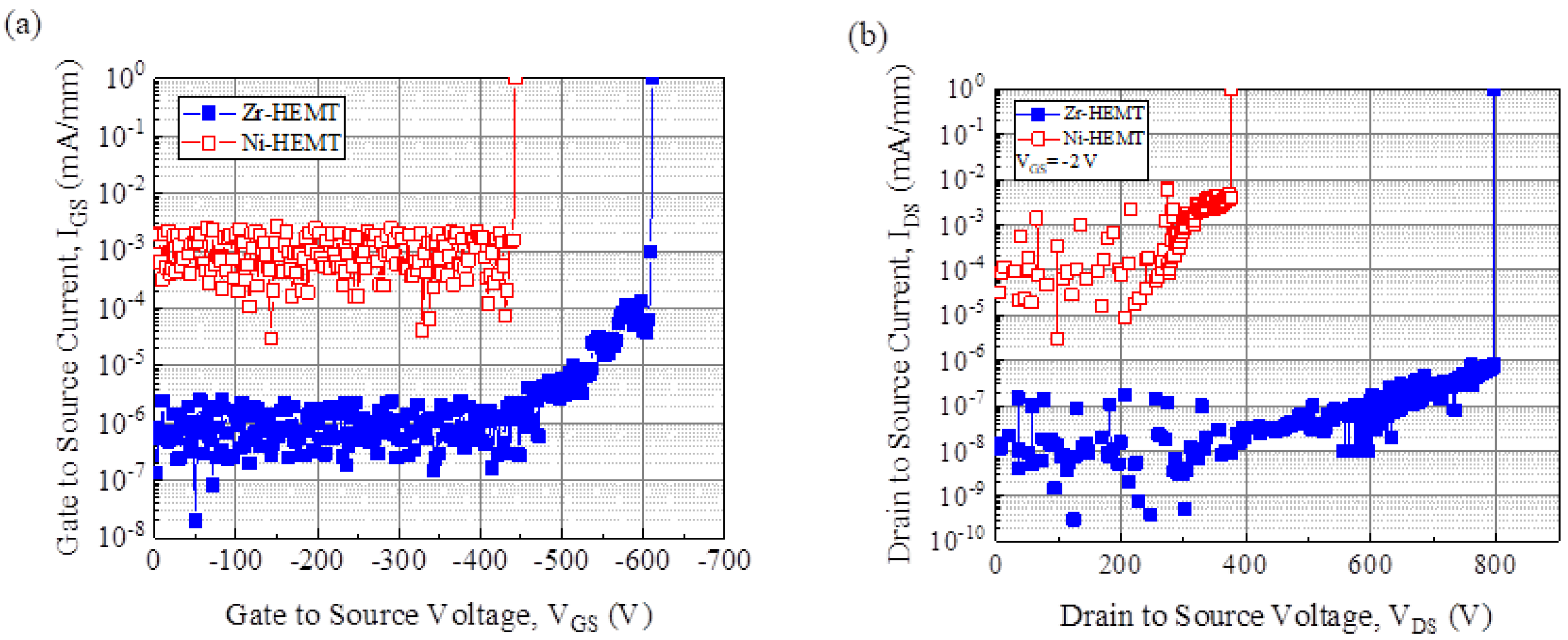
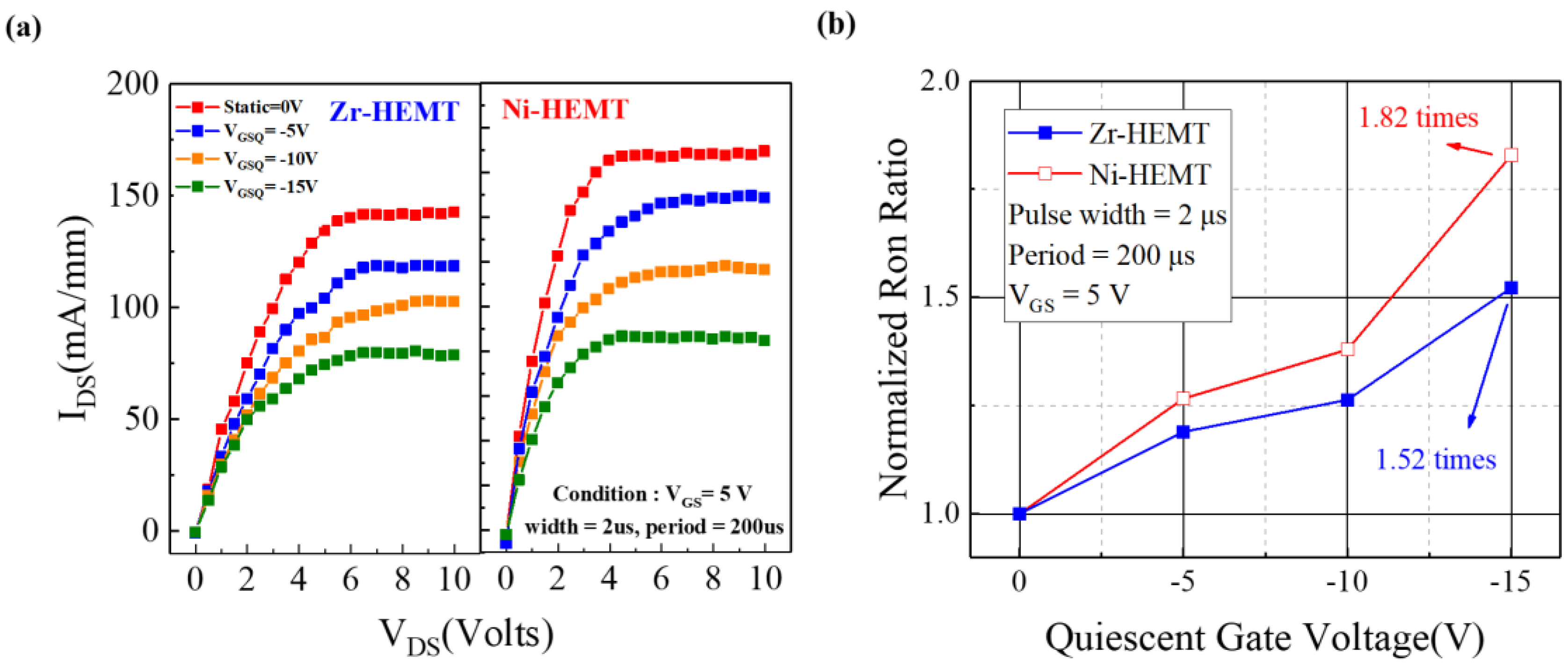
3. Experimental Result and Discussion
4. Conclusions
Author Contributions
Funding
Conflicts of Interest
References
- Uemoto, Y.; Hikita, M.; Ueno, H.; Matsuo, H.; Ishida, H.; Yanagihara, M.; Ueda, T.; Tanaka, T.; Ueda, D. Gate injection transistor (GIT) normally-off AlGaN/GaN power transistor using conductivity modulation. IEEE Trans. Electron Devices 2007, 54, 3393–3399. [Google Scholar] [CrossRef]
- Saito, W.; Takada, Y.; Kuraguchi, M.; Tsuda, K.; Omura, I.; Ogura, T.; Ohashi, H. High breakdown voltage AlGaN–GaN power-HEMT design and high current density switching behavior. IEEE Trans. Electron Devices 2003, 50, 2528–2531. [Google Scholar] [CrossRef]
- Cai, Y.; Zhou, Y.; Chen, K.J.; Lau, K.M. High-performance enhancement-mode AlGaN/GaN HEMTs using fluoride-based plasma treatment. IEEE Electron Device Lett. 2005, 26, 435–437. [Google Scholar] [CrossRef]
- Tang, Z.; Jiang, Q.; Lu, Y.; Huang, S.; Yang, S.; Tang, X.; Chen, K.J. 600-V normally off SiNx /AlGaN/GaN MIS-HEMT with large gate swing and low current collapse. IEEE Electron Device Lett. 2013, 34, 1373–1375. [Google Scholar] [CrossRef]
- Hu, X.; Simin, G.; Yang, J.; Khan, M.A.; Gaska, R.; Shur, M.S. Enhancement mode AlGaN/GaN HFET with selectively grown pn junction gate. Electron. Lett. 2000, 36, 753–754. [Google Scholar] [CrossRef]
- Hilt, O.; Knauer, A.; Brunner, F.; Bahat-Treidel, E.; Würfl, J. Normally-off AlGaN/GaN HFET with p-type Ga gate and AlGaN buffer. In Proceedings of the 24th International Symposium on Power Semiconductor Devices & ICs, Hiroshima, Japan, 6–10 June 2010; pp. 347–350. [Google Scholar]
- Wu, T.-L.; Marcon, D.; You, S.; Posthuma, N.; Bakeroot, B.; Stoffels, S.; Hove, M.V.; Groeseneken, G.; Decoutere, S. Forward bias gate breakdown mechanism in enhancement-mode p-GaN gate AlGaN/GaN high-electron mobility transistors. IEEE Electron Device Lett. 2015, 36, 1001–1003. [Google Scholar] [CrossRef]
- Hwang, I.; Choi, H.; Lee, J.; Choi, H.S.; Kim, J.; Ha, J.; Um, C.-Y.; Hwang, S.-K.; Oh, J.; Kim, J.-Y.; et al. 1.6 kV, 2.9 mohm.cm2 normally-off p-GaN HEMT device. In Proceedings of the 24th International Symposium on Power Semiconductor Devices & ICs, Bruges, Belgium, 3–7 June 2012; pp. 41–44. [Google Scholar] [CrossRef]
- Saito, W.; Takada, Y.; Kuraguchi, M.; Tsuda, K.; Omura, I. Recessed gate structure approach toward normally off high-voltage AlGaN/GaN HEMT for power electronics applications. IEEE Trans. Electron Devices 2006, 53, 356–362. [Google Scholar] [CrossRef]
- Li, W.; Zhang, Z.; Fu, K.; Yu, G.; Zhang, X.; Sun, S.; Song, L.; Hao, R.; Fan, Y.; Cai, Y.; et al. Design and simulation of a novel E-mode GaN MISHEMT based on a cascode connection for suppression of electric field under gate and improvement of reliability. J. Semicond. 2017, 38, 074001. [Google Scholar] [CrossRef]
- Roccaforte, F.; Vivona, M.; Nigro, R.L.; Giannazzo, F.; di Franco, S.; Bongiorno, C. Ti/Al-based contacts to p-type SiC and GaN for power device applications. Phys. Status Solid A 2017, 214, 1600357. [Google Scholar] [CrossRef]
- Hwang, I.; Kim, J.; Choi, H.S.; Choi, H.; Lee, J.; Kim, K.Y.; Park, J.-B.; Lee, J.C.; Ha, J.; Oh, J.; et al. p-GaN Gate HEMTs with Tungsten Gate Metal for High Threshold Voltage and Low Gate Current. IEEE Electron Device Lett. 2013, 34, 202–204. [Google Scholar] [CrossRef]
- Noda, N.; Tsurumaki, R.; Horio, K. Analysis of lags and current collapse in field-plate AlGaN/GaN HEMTs with deep acceptors in a buffer layer. Phys. Status Solidi C 2016, 13, 341. [Google Scholar] [CrossRef]
- Chiu, H.-C.; Chang, Y.-S.; Li, B.-H.; Wang, H.-C.; Kao, H.-L. High-Performance Normally Off p-GaN Gate HEMT with Composite AlN/Al0.17Ga0.83N/Al0.3Ga0.7N Barrier Layers Design. J. Electron Device Soc. 2018, 6, 201–206. [Google Scholar] [CrossRef]
- Wang, H.; Wei, J.; Xie, R.; Liu, C.; Tang, G.; Chen, K.J. Maximizing the Performance of 650-V p-GaN Gate HEMTs: Dynamic RON Characterization and Circuit Design Considerations. IEEE Trans. Power Electron. 2017, 32, 5539–5549. [Google Scholar] [CrossRef]


© 2020 by the authors. Licensee MDPI, Basel, Switzerland. This article is an open access article distributed under the terms and conditions of the Creative Commons Attribution (CC BY) license (http://creativecommons.org/licenses/by/4.0/).
Share and Cite
Liu, C.-H.; Chiu, H.-C.; Huang, C.-R.; Chang, K.-J.; Chen, C.-T.; Hsueh, K.-P. Low Gate Lag Normally-Off p-GaN/AlGaN/GaN High Electron Mobility Transistor with Zirconium Gate Metal. Crystals 2020, 10, 25. https://doi.org/10.3390/cryst10010025
Liu C-H, Chiu H-C, Huang C-R, Chang K-J, Chen C-T, Hsueh K-P. Low Gate Lag Normally-Off p-GaN/AlGaN/GaN High Electron Mobility Transistor with Zirconium Gate Metal. Crystals. 2020; 10(1):25. https://doi.org/10.3390/cryst10010025
Chicago/Turabian StyleLiu, Chia-Hao, Hsien-Chin Chiu, Chong-Rong Huang, Kuo-Jen Chang, Chih-Tien Chen, and Kuang-Po Hsueh. 2020. "Low Gate Lag Normally-Off p-GaN/AlGaN/GaN High Electron Mobility Transistor with Zirconium Gate Metal" Crystals 10, no. 1: 25. https://doi.org/10.3390/cryst10010025