1. Introduction
Different metal-oxide thin films are increasingly applied for a wide range of optical and microelectronic applications. In those materials, the most stable form of niobium oxides is Nb
2O
5 and it is very attractive for electronic and optical applications. Nb
2O
5, along with other oxides of metals from the Vth group, have also been investigated as possible candidates for thin film catalysts and corrosion barrier coatings [
1,
2]. In the case of optical applications, Nb
2O
5-based thin films are often used as high index and low loss materials; for example, they can be used as optical waveguides [
3,
4], interference filters, antireflective or antireflection (AR) coatings or electroluminescent devices [
5,
6,
7]. An AR coating is a type of optical coating applied to the surface of lenses and other optical elements to reduce reflection. For example, bare silicon–based solar cells have a high surface reflection of over 30%. AR coatings are applied to reduce surface reflection and maximize the devices’ efficiency for the solar cells manufactured on glass and silicon substrates [
8]. The simplest interference antireflection (AR) coating can be achieved by using a single quarter-wave layer of oxide thin films whose refractive index is chosen as the square root of the substrate’s refractive index. The single-layer AR coating consists of a dielectric thin film. As the thin films have a specially chosen thickness, the interference effects in the AR coating will cause the wave to be reflected from the top surface of the coating layers to be out of phase with the wave reflected from the surfaces of the semiconductor [
9]. For that, the thin films can have an effect of zero reflectance at the center light wavelength which can decrease reflectance for light wavelengths in a broad band around the center. As the multi-layer AR coating thin films are used, the alternating layers of a low-index material (such as SiO
2) and a higher-index material (such as ZrO
2) are possible to obtain reflectivity as low as 0.1% at a special or single wavelength [
10,
11].
Nb
2O
5 is one of the useful optical thin-film materials because of its desirable properties, including stability in air and water and resistance to acids and bases. Also, the Nb
2O
5 thin films have the properties of high refractive index, low extinction coefficient, and high transparent ratio in the UV-vis-NIR (ultraviolet-visible near-infrared) region [
12,
13]. The properties of Nb
2O
5 thin films closely rely on the sputtered materials, deposition techniques, deposition parameters, and the thicknesses of thin films. For that, many different methods are investigated to deposit Nb
2O
5 thin films. For example, Nb
2O
5 thin films can be deposited on variety of substrates using the sol-gel dip coating technique [
14], and the deposited Nb
2O
5 thin films revealed an amorphous phase [
1,
15,
16]. Agarwal and Reddy found that after annealing Nb
2O
5 thin films under controlled ambience at 600 °C for 5 h, the thin films deposited on NaCl substrates crystallized into a stable monoclinic phase and those deposited on single-crystal Si substrates crystallized into a hexagonal phase [
13]. The optical band gap of Nb
2O
5 thin films increased from 4.35 eV when the films were in an amorphous state to 4.87 eV on crystallization [
13]. Lazarova et al. obtained Nb
2O
5 thin films by mixing NbCl
5 with ethanol to form the spin-coating precursor. The mixing material was spin-coated on glass and silicon substrates and then they were annealed at different temperatures to obtain the Nb
2O
5 thin films [
17]. Nb
2O
5 thin films could also be formed by annealing the sputter-deposited Nb thin films under a pure Ar flow plasma and annealing them in a quartz tube at 850 °C. Jose et al. observed vibrational modes including longitudinal optical, transverse optical, and triply degenerate modes, and found the direct optical band gap to be ~3.49 eV [
18].
Sputtering is a simple method to deposit Nb
2O
5 thin films with a controllable thickness [
19]. In the sputtering method, the properties of the Nb
2O
5 thin films depend on the deposition parameters, such as the deposition temperature [
20], reactive gas flow or pressure. In this paper, Nb
2O
5 thin films were deposited on glass substrates by using the sputtering method. The effects of the deposition temperature and oxygen concentration (10% and 20%) in the deposition atmosphere on the properties of Nb
2O
5 thin films were investigated by X-ray diffraction (XRD) patterns and field emission scanning electron microscopy (FESEM), respectively. In this paper we found two important novelties. The first novelty in this paper is that the Nb
2O
5 thin films deposited in pure argon atmosphere revealing an un-transparent result. The second novelty is that the O
2 flow rate has a large effect on the properties of Nb
2O
5 thin films; only a few studies focused on the effect of the O
2 flow rate on that topic. In the past, the Nb
2O
5 thin films had been investigated by different methods, for example by the microwave-assisted reactive magnetron sputtering process [
6], by the glancing angle deposition process [
12], by the sol-gel dip coating technique [
13], by the sol-gel and evaporation-induced self-assembly method [
14], by radio frequency (RF) magnetron sputtering [
16], and by a low frequency reactive magnetron sputtering system [
19], respectively. In the past, as the physical plasma method was used to deposit the Nb
2O
5 thin films, no reports were focused on the effect of the O
2 flow rate in the (O
2 + Ar) mixing atmosphere on the properties’ extinction coefficient, optical band gap (
Eg) values, and refractive index. Coskuna et al. used the RF magnetron sputtering method to deposit the Nb
2O
5 thin films [
16], and they investigated the effect of the deposition temperature but they did not investigate the effect of the O
2 flow rate on the properties of Nb
2O
5 thin films. Mazur et al. used the microwave-assisted reactive magnetron sputtering process [
6] and Lai et al. used the low frequency reactive magnetron sputtering system [
19] to deposit the Nb
2O
5 thin films by using a metallic Nb target in the O
2 + Ar mixing atmosphere, and they also did not investigate the effect of the O
2 flow rate on the properties of Nb
2O
5 thin films.
RF magnetron sputtering is a well-established high-rate vacuum coating method for the deposition of industrial thin film materials and the thickness of deposited thin films can be well controlled by controlling the deposition parameters. For that, we used RF magnetron sputtering and the Nb2O5 ceramic target to deposit the Nb2O5 thin films. We found that the O2 flow rate had a large effect on the transmittance and reflectance of Nb2O5 thin films. Additionally, optical properties of Nb2O5 thin films, such as transmittance, reflectance, and reactance, were determined by using a spectrophotometer and elliposmeter. The second novelty is that we discussed different O2 flow rates in the (O2 + Ar) mixing atmosphere to investigate its effect on the properties of Nb2O5 thin films, especially on the extinction coefficient, optical band gap (Eg) values, and refractive index. For example, the refractive index of Nb2O5 thin films increased with the increase of the O2 flow rate in the (O2 + Ar) mixing atmosphere. The results in this study show that the Nb2O5 antireflective layer with protective properties can be proposed for possible use in silicon solar cells.
3. Results and Discussion
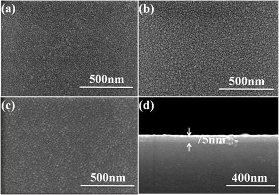
Figure 1 shows the surface and cross-section observations of Nb
2O
5 thin films with various deposition temperatures and the O
2 ratio was 10%. As the results in
Figure 1 show, high resolution SEM reveals that when the deposition temperature was RT, there was a densified surface morphology, consisting of nanocrystalline particles growing in a random orientation. Further increasing the deposition temperature to 300 and 400 °C caused the Nb
2O
5 thin films to have larger nanocrystalline grains. Even when the O
2 ratio was changed to 20%, the variations in the surface morphology of the Nb
2O
5 thin films had similar results, and the sizes of the nanocrystalline grains increased (not shown here). The root mean square (RMS) surface roughness of the Nb
2O
5 thin films was measured to be 0.30 nm by AFM. When the deposition temperature was RT, 200, 300 and 400 °C, the measured values were 2.56, 3.46, 4.39 and 5.25 nm when the O
2 ratio was 10% and the measured values were 2.44, 3.32, 4.24 and 5.08 nm when the O
2 ratio was 20%, respectively. Apparently, the roughness increased as the deposition temperature was raised. Apparently, the results show that the roughness of the Nb
2O
5 thin films increased with the increasing deposition temperature. The results in
Figure 1 have also revealed an important result: that the nanocrystalline grains had uniform particle sizes. The average crystallite sizes of Nb
2O
5 thin films can be calculated using the following equation:
where
G is the number of grains per unit area at a particular magnification,
N is the number of grains/mm
2. The average crystallite sizes were about 12.3, 16.5, 22.7 and 34.5 nm when the deposition temperatures were RT (
Figure 1a), 200 °C (not shown here), 300 °C (
Figure 1b), and 400 °C (
Figure 1c), respectively. When the O
2 ratio was 20%, the average crystallite sizes were about 11.2, 15.1, 21.4 and 32.5 nm when the deposition temperatures were RT, 200 °C, 300 °C, and 400 °C, respectively (not shown here).
The average crystallite sizes and the deviation of the crystallite sizes of Nb
2O
5 thin films are shown in
Table 1. We believe that the higher deposition temperature will cause the Nb
2O
5 molecules to have a large activation energy and then the Nb
2O
5 thin films have a larger particle size and larger roughness. The thickness of Nb
2O
5 thin films is also observed and the result is shown in
Figure 1d. The thickness was around 75 nm when the deposition temperature was 200 °C and the O
2 ratio was 10%, respectively. We found that as the deposition temperature was changed from RT to 400 °C and the O
2 ratio was 10% and 20%, the average thicknesses of Nb
2O
5 thin films were in the range of 72.7–77.7 nm and 46.4–47.9 nm, respectively. The average thicknesses and the deviation of the thicknesses of Nb
2O
5 thin films are also shown in
Table 1. Those results suggest that in this study, the O
2 ratio has no effect but the deposition temperature has apparent effect on the surface morphology, and the O
2 ratio has an effect but the deposition temperature has no apparent effect on the thickness, respectively.
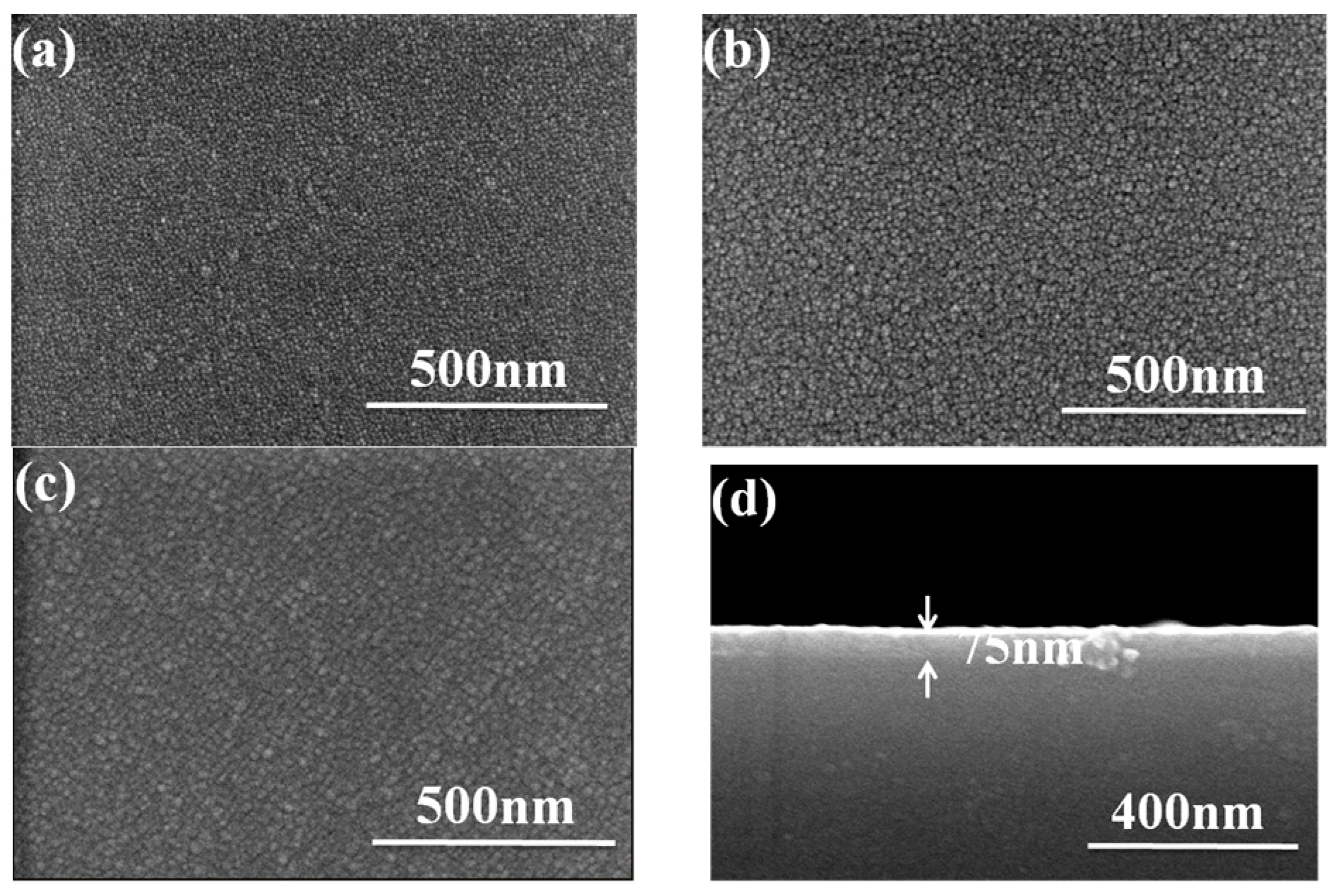
The XRD patterns of Nb
2O
5 thin films developed as a function of deposition temperatures are shown in
Figure 2a, where the oxygen concentration was 10%. As the different sintering temperatures were used, the differently crystalline phases would be formed in the Nb
2O
5 ceramic targets, and the multi-crystal phases were only observed in the Nb
2O
5 ceramic targets. Nb
2O
5 thin films deposited by the sputtering method in the O
2/Ar mixed atmosphere would reveal the amorphous phase rather than the polycrystal phase since no characteristic peaks were observed in the XRD patterns. The amorphous nature of the deposited thin films can result from the low temperature of the sputtering process. Even when the Nb
2O
5 thin films were deposited at 400 °C, the deposition temperature was not high enough to crystallize the Nb
2O
5 thin films.
Figure 2b shows that when the oxygen concentration was 20% and the deposition temperature was 400 °C, the XRD patterns of Nb
2O
5 thin films also revealed the amorphous phase.
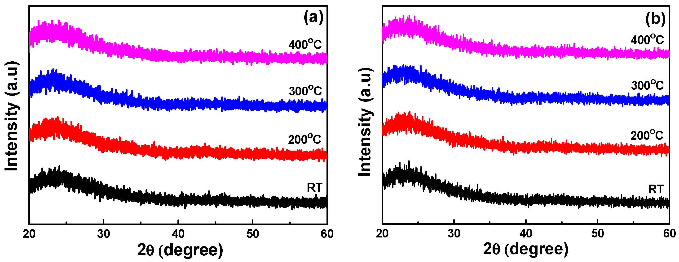
The transmittance of Nb
2O
5 thin films under various deposition temperatures and O
2 ratios is depicted in
Figure 3. When the O
2 ratio was 10%, the average total transmittance of the RT-deposited Nb
2O
5 thin films was 74.42%, whereas the Nb
2O
5 thin films showed that the average total transmittance was almost unchanged with the increasing deposition temperature in the visible-light wavelength (400–800 nm) region. The average total transmittances of 74.15%, 73.87%, and 75.17% were shown as the deposition temperature was 200, 300 and 400 °C, respectively. The maximum transmittance ratio was 85.73% at 361 nm, 90.78% at 382 nm, 91.06% at 387 nm, and 91.54% at 402 nm, respectively. However, when the O
2 ratio was 20%, the average total transmittances of the Nb
2O
5 thin films had different results. When the deposition temperature was RT, 200, 300 and 400 °C, the average total transmittance was 73.82%, 69.90%, 68.42%, and 64.72%, respectively. Apparently, the average total transmittances of the Nb
2O
5 thin films decreased with the increasing deposition temperature in the visible-light wavelength region. The results in
Figure 3b also show that the transmittance of the Nb
2O
5 thin films increased with the increasing measuring frequency. The red-shift of the maximum transmittance in Nb
2O
5 thin films was also apparently observed as the deposition temperature increased. When the same deposition temperature was used, in the transmission spectra of the 20% O
2-deposited Nb
2O
5 thin films, the optical band edge was also shifted to a shorter light wavelength. The optical transmittance properties of Nb
2O
5 thin films are listed in
Table 2.
When the oxygen ratio was 10% and the deposition temperature increased from RT to 400 °C, the optical band edges in the transmission spectra of the Nb
2O
5 thin films were shifted to a longer light wavelength and a greater sharpness was noticeable in the curves of the absorption edges. Those results mean that as the deposition temperature increases, the absorption edge of the Nb
2O
5 thin films is red-shifted. In the past, the determination of the optical band gap (
Eg) was often necessary to develop the electronic band structure of a thin film material. Typically, a Tauc plot shows the quantity
hν (the photon energy) on the abscissa and the quantity (α
hν)
r on the ordinate, where α is the optical absorption coefficient,
c is the constant for direct transition,
h is Planck’s constant,
ν is the frequency of the incident photon, and the exponent
r denotes the nature of the transition [
21]. When using the Tauc plot method, the
Eg values of thin films can be determined from the absorption edge for the direct interband transition, which can be calculated using the relation in Equation (1) [
21]:
where α is the optical absorption coefficient,
c is the constant for direct transition,
h is Planck’s constant, and
ν is the frequency of the incident photon [
21].
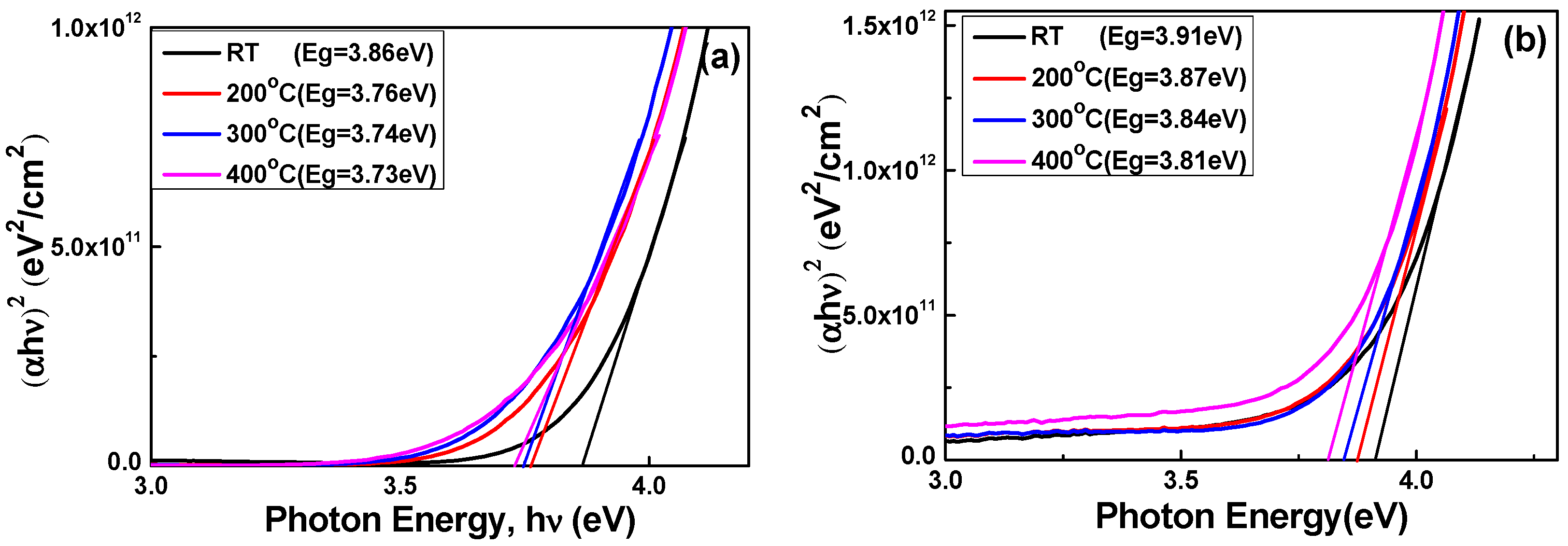
Figure 4 shows the energy band gap of the plasma-treated Nb
2O
5 thin films plotted against light wavelengths in the region of 300–1000 nm. The linear dependence of (α
hv)
2 on
hν indicates that Nb
2O
5 thin films are a direct transition material [
21]. The experimental band-gap width of Nb
2O
5 is generally measured in the order of 3.3 to 3.9 eV [
22,
23]. In accordance with Equation (1), the calculated optical band gap of the Nb
2O
5 thin films decreased from 3.86 to 3.73 eV when the O
2 ratio was 10% and decreased from 3.91 to 3.81 eV when the O
2 ratio was 20%. As the results in
Figure 4a,b were compared, we found that as the same deposition temperature was used to deposit Nb
2O
5 thin films, the
Eg value for using the O
2 ratio of 20% was higher than that for using the O
2 ratio of 10%.
The optical band gap of amorphous materials depends on their structure and components; thus, it is closely related to the deposition techniques. For a transparent material or thin film, when the light wavelength is equal to 300 nm, the visible light absorbed by the thin films is due to a quantum phenomenon called band edge absorption [
24]. In this study, the thicknesses of Nb
2O
5 thin films are about 75 nm when the O
2 ratio is 10% and about 47 nm when the O
2 ratio is 20%. Because the thicknesses of Nb
2O
5 thin films are smaller than 300 nm, the band edge absorption effect will not happen. We believed that the decrease in the band gap with the increased deposition temperature could be attributed to a shift in either the conduction or valence bands leading to narrower energy band gaps. In the past, the red-shift effect could be explained by the Burstein-Moss shift, a shift of the Fermi level into the conduction band, which enhances the optical band gap by the energy, as follows [
25,
26]:
where
kF stands for the Fermi wave vector,
me is the effective mass of electrons in the conduction band, and
mh is the effective mass of holes in the valence band. The Nb
2O
5 thin films are an insulating material as the oxygen is introduced during the deposition process. For that, the Burstein-Moss shift is not the reason that causes the increase in the value of the optical band gap. The formal Nb-oxidation state of Nb
2O
5 is +5 and the corresponding electronic configuration of the Nb atoms is [Kr]4d
0, i.e., all of the d-electrons have been transferred to the O
2p band and the Nb
4d band is empty [
23]. Moreover, Brayner et al. experimentally observed that the energy of the absorption edge is influenced not only by the number of interconnected polyhedrals (size effect) but also by the local coordination as the particle sizes decrease from about 40 to 4.5 nm. They also found that the transmission spectrum shows a significant blue shift of the absorption edge and an increase of the optical band gap from 3.4 to 4.2 eV as the size of the Nb
2O
5 particles decreases from about 40 to 4.5 nm. They ascribed this modification to a quantum-size effect [
27].
Figure 1 shows that particle sizes of the Nb
2O
5 thin films increased with the increasing deposition temperature and
Figure 4 shows that the values of the optical band gap decreased with the increasing deposition temperature. We believe that as the deposition temperature increases, the quantum-size effect is the reason that causes the decrease in the optical band gap values of Nb
2O
5 thin films.
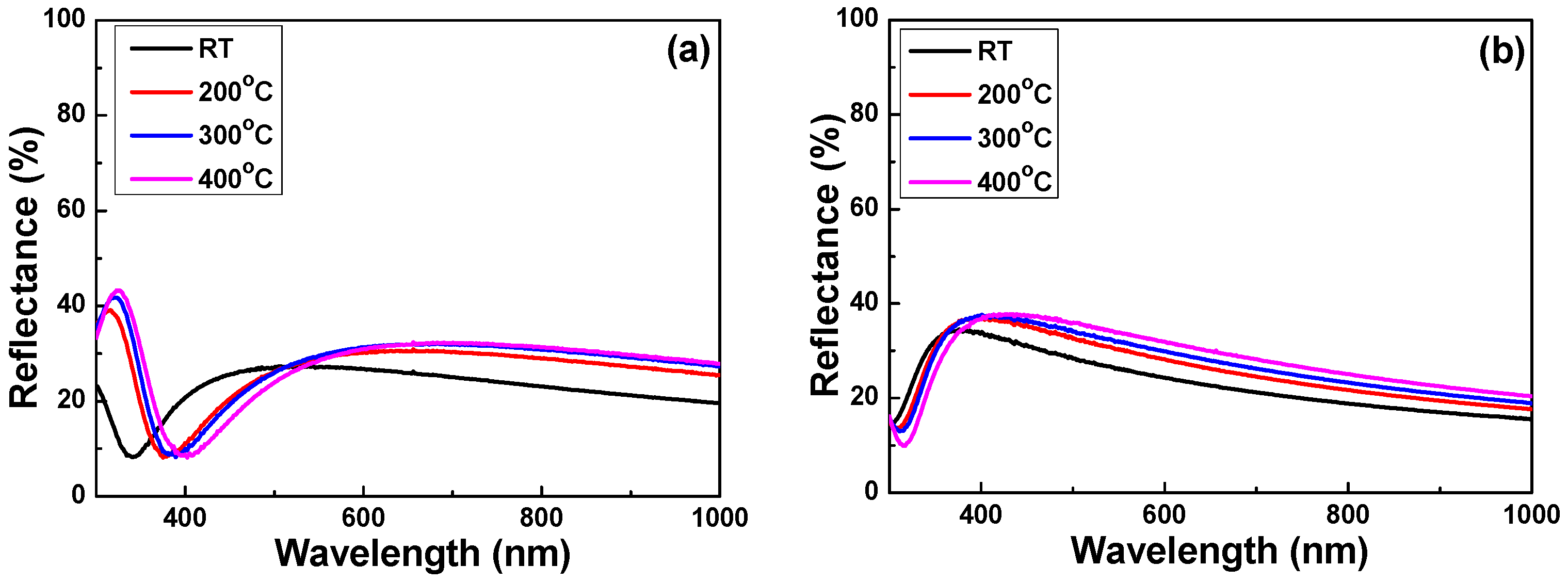
Reflectance is a ratio of the intensity of the incident optical light or other electromagnetic radiation on the surface of a material or a thin film. As usual, the reflectance spectrum can be plotted as a function of the light wavelength.
Figure 5 shows the measured reflectance of Nb
2O
5 thin films as a function of the deposition temperature and the O
2 ratio in the light wavelength range of 350–1000 nm. As we know, reflectivity can be defined as the square of the magnitude of the Fresnel reflection coefficient [
28], which is the ratio of the reflected electric field to incident on a material or a thin film. If the reflection occurs from a thin layer of materials and the thicker the sample that is used, the effects of the internal reflection can cause the measured reflectance to change as the surface thickness and reflectivity are the limit values of reflectance. As the spectrum in
Figure 5a shows, as the O
2 ratio was 10%, the average reflectances of 26.0%, 26.3%, 26.6%, and 25.3% were shown as the deposition temperature was RT, 200, 300 and 400 °C.
The reflectance first increased as the light wavelength increased and reached a maximum at around 325 nm (except the RT-deposited thin films), then it decreased and reached a minimum at around 400 nm. The minimum reflectance was 8.13% in the 400 °C–deposited Nb
2O
5 thin films. As the spectrum in
Figure 5b shows, when the O
2 ratio was 20%, the average reflectances of 26.7%, 30.6%, 32.0%, and 33.7% were shown as the deposition temperature was RT, 200, 300 and 400 °C, respectively. The reflectance first increased as the light wavelength increased and the reflectance reached a maximum when the light wavelength was around 400 nm. When the light wavelength increased from 400 to 1000 nm, the reflectance linearly decreased. The results shown in
Figure 3 and
Figure 5 suggest that the O
2 ratio is an important factor that affects the optical properties of Nb
2O
5 thin films. The red-shift of the minimum reflectance in the Nb
2O
5 thin films was also apparently observed as the deposition temperature increased. The optical reflectance properties of Nb
2O
5 thin films are listed in
Table 3.
In optics, the refractive index or index of refraction
n of an optical medium is a dimensionless number that describes how light, or any other radiation, propagates through that medium. It is defined as:
where
c is the speed of light in a vacuum and
v is the phase velocity of light in the medium. The refractive index is not a stable value and it will vary with the light wavelength. That is called dispersion and it causes the splitting of white light into its constituent colors into rainbows and chromatic aberration in lenses. However, the light propagation in absorbing materials is very complicated and can be described using a complex-valued refractive index. We can measured the refractive index by using n&k Analyzer 1280 and
Figure 6 shows the measured refractive index of Nb
2O
5 thin films as a function of the deposition temperature and O
2 ratio.
No matter whether the O
2 ratio was 10% or 20%, the refractive index of the Nb
2O
5 thin films decreased with the increasing light wavelength. For example, as
Figure 6a shows for when O
2 ratio was 10%, the refractive index decreased from 3.14 to around 2.3 when light wavelength was longer than 450 nm and then the refractive index had a stable value when the light wavelength was longer.
Figure 6b (when O
2 ratio was 20%) also shows that the refractive index at the same light wavelength increased as the deposition temperature was increased from RT to 200 °C and slightly increased as the deposition temperature was further increased. As
Figure 6b shows, the variation in the refractive index of Nb
2O
5 thin films was similar to that of Nb
2O
5 thin films with an O
2 ratio of 10%. As the results in
Figure 6 are compared, we have found that as the same deposition temperature was used, the refractive index of the Nb
2O
5 thin films deposited with the O
2 ratio of 20% was higher than that deposited with the O
2 ratio of 10%. Those results suggest again that the deposition temperature and O
2 ratio are two important factors that will affect the properties of Nb
2O
5 thin films. Those results suggest that as a higher substrate temperature is used to deposit Nb
2O
5 thin films, the probability of collisions between atoms is high and this results in the sputtered atoms having higher energies, so they can easily diffuse and the thin films’ structure is more compact. Thus, the refractive index is relatively high. On the contrary, when a lower substrate temperature is used to deposit the Nb
2O
5 thin films, the structure becomes less densified and the refractive index would be expected to be lower; therefore, the results of the experiments are as expected. The refractive index values of the Nb
2O
5 thin films investigated increased from 2.14 to 2.34 when the O
2 ratio was 10% and increased from 2.18 to 2.44 when the O
2 ratio was 20%. When the deposition temperature was RT and 200 °C, the refractive index values of the Nb
2O
5 thin films were lower than the values revealed in Reference [
19], which changed from 2.23 to 2.28. In the past, there was no research using both the deposition temperature and O
2 ratio (or they only used the O
2 ratio) as the deposition parameters. We believe that the high refractive index values in this study are caused by the use of O
2 during the deposition process, and this will compensate for the oxygen defects in the Nb
2O
5 thin films.
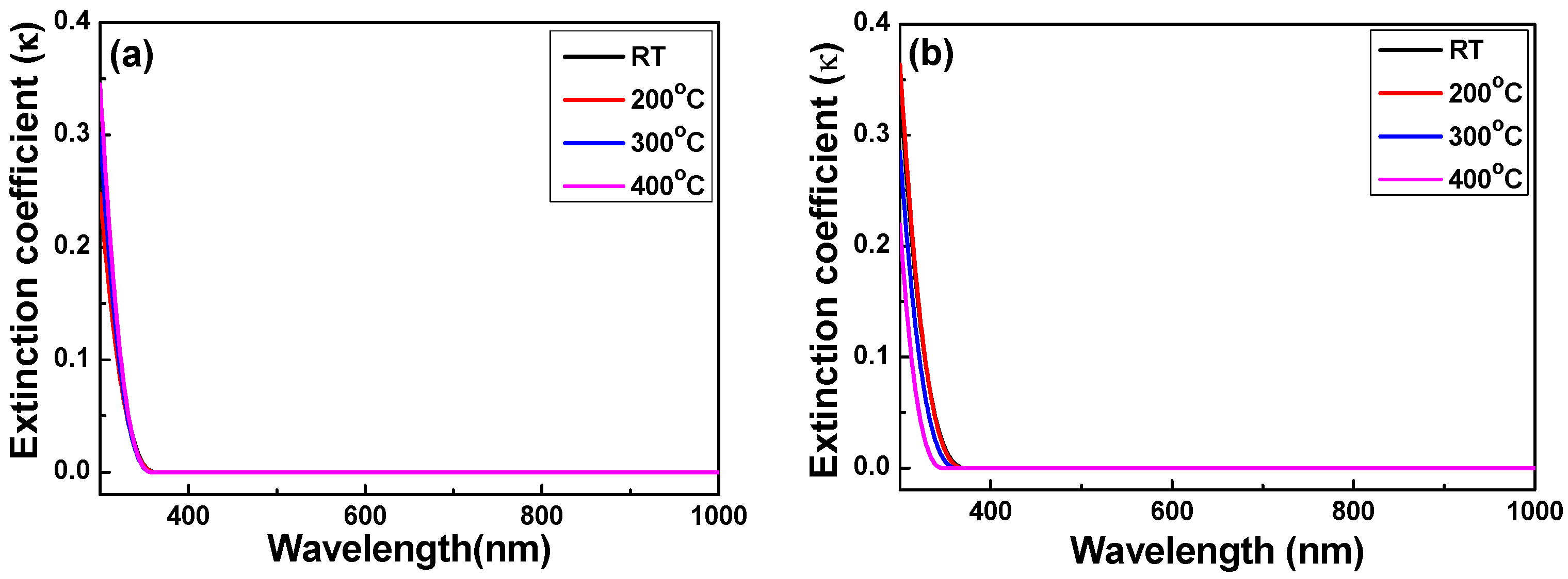
Forouhi and Bloomer deduced dispersion equations for the refractive index,
n, and the extinction coefficient,
k [
7,
29]. The refractive index (
n) and extinction coefficient (
k) are related to the interaction between a material and incident light, and are associated with refraction and absorption. Those descriptions suggest again that the properties of the extinction coefficient of Nb
2O
5 thin films are very complicated.
Figure 7 shows the extinction coefficient of Nb
2O
5 thin films as a function of the deposition temperature and the O
2 ratio in a spectrum range of 350–1000 nm. As the light wavelength changed, the extinction coefficient linearly decreased from ~0.35 when the light wavelength was 350 nm to smaller than 10
−4 when light wavelength was longer than the 361 nm. When the O
2 ratio was 10% and the deposition temperature was RT, 200, 300 and 400 °C, the extinction coefficient was 4.05 × 10
−5, 9.40 × 10
−5, 4.82 × 10
−5, and 2.75 × 10
−5 when the light wavelength was 361, 360, 358 and 357 nm, and the extinction coefficient was zero when the light wavelength was longer than 362, 361, 358 and 357 nm; when the O
2 ratio was 20% and the deposition temperature was RT, 200 °C, 300 °C, and 400 °C, the extinction coefficient was 2.75 × 10
−5, 9.81 × 10
−5, 1.68 × 10
−5 and 6.89 × 10
−5 when the light wavelength was 370, 367, 361 and 345 nm, and the extinction coefficient was zero when the light wavelength was longer than 370, 368, 361 and 346 nm, respectively. The extinction coefficient apparently decreases as the deposition temperature increases and it has no apparent trend as the O
2 ratio is changed. The results in
Figure 5 suggest that Nb
2O
5 thin films are stable dielectric films with a low extinction coefficient in the range of visible light.


