
21.69–24.36 GHz MEMS Tunable Band-Pass Filter

Abstract
:
1. Introduction
2. Filter Design
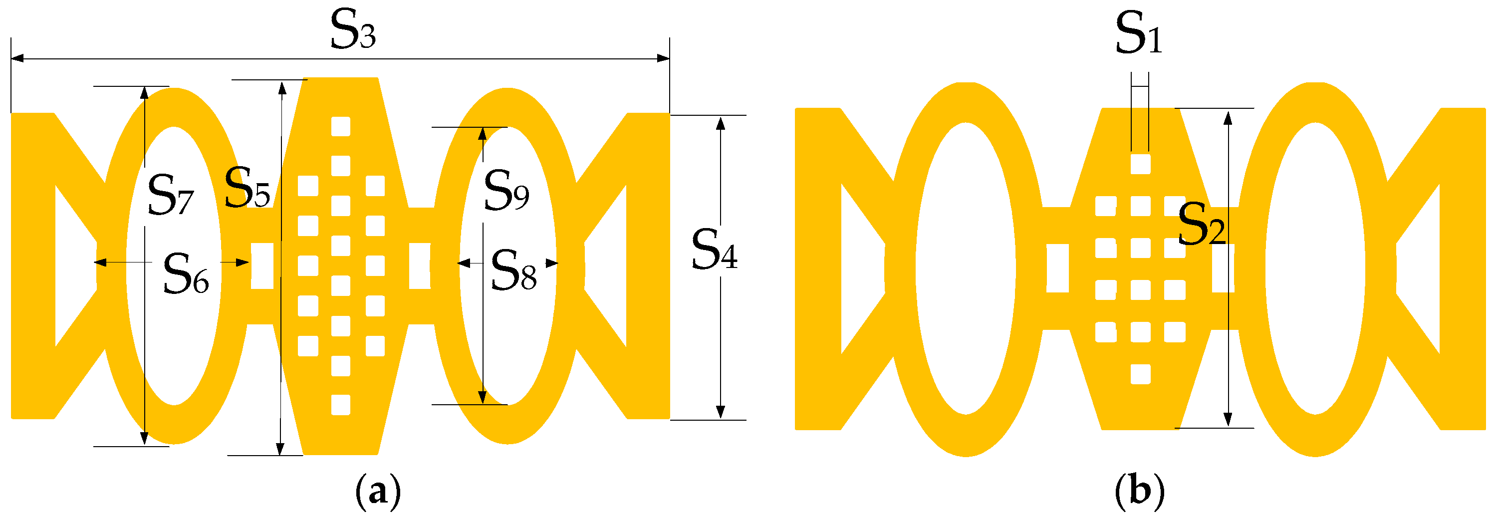
2.1. Topology
2.2. Filter Structure and Tunable Mechanism
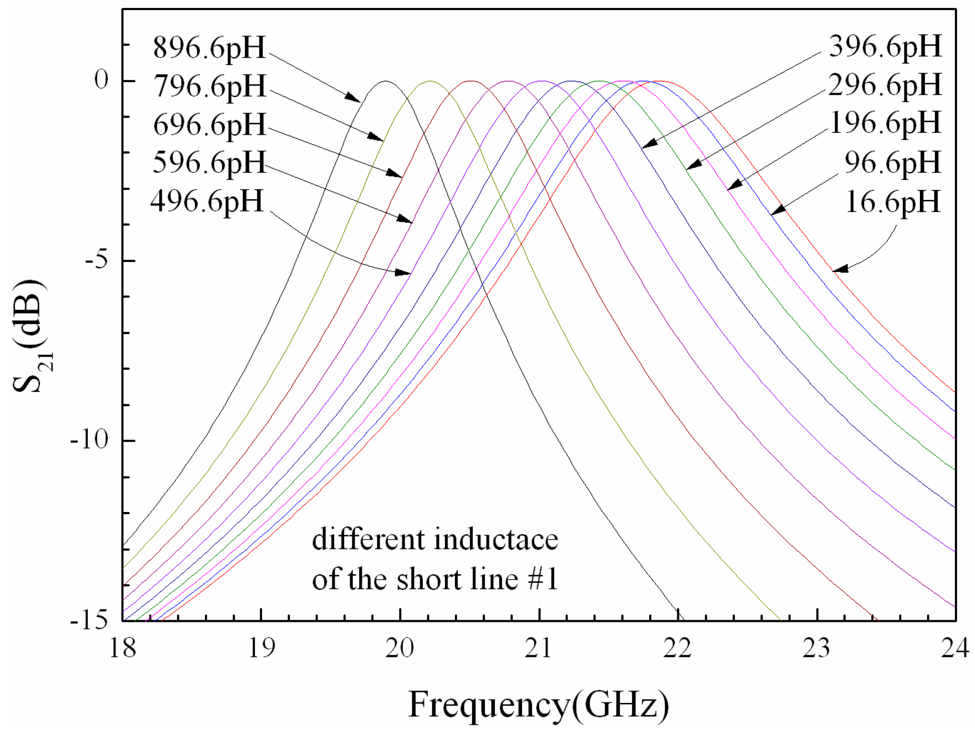
2.3. Parameters Calculation and Simulations
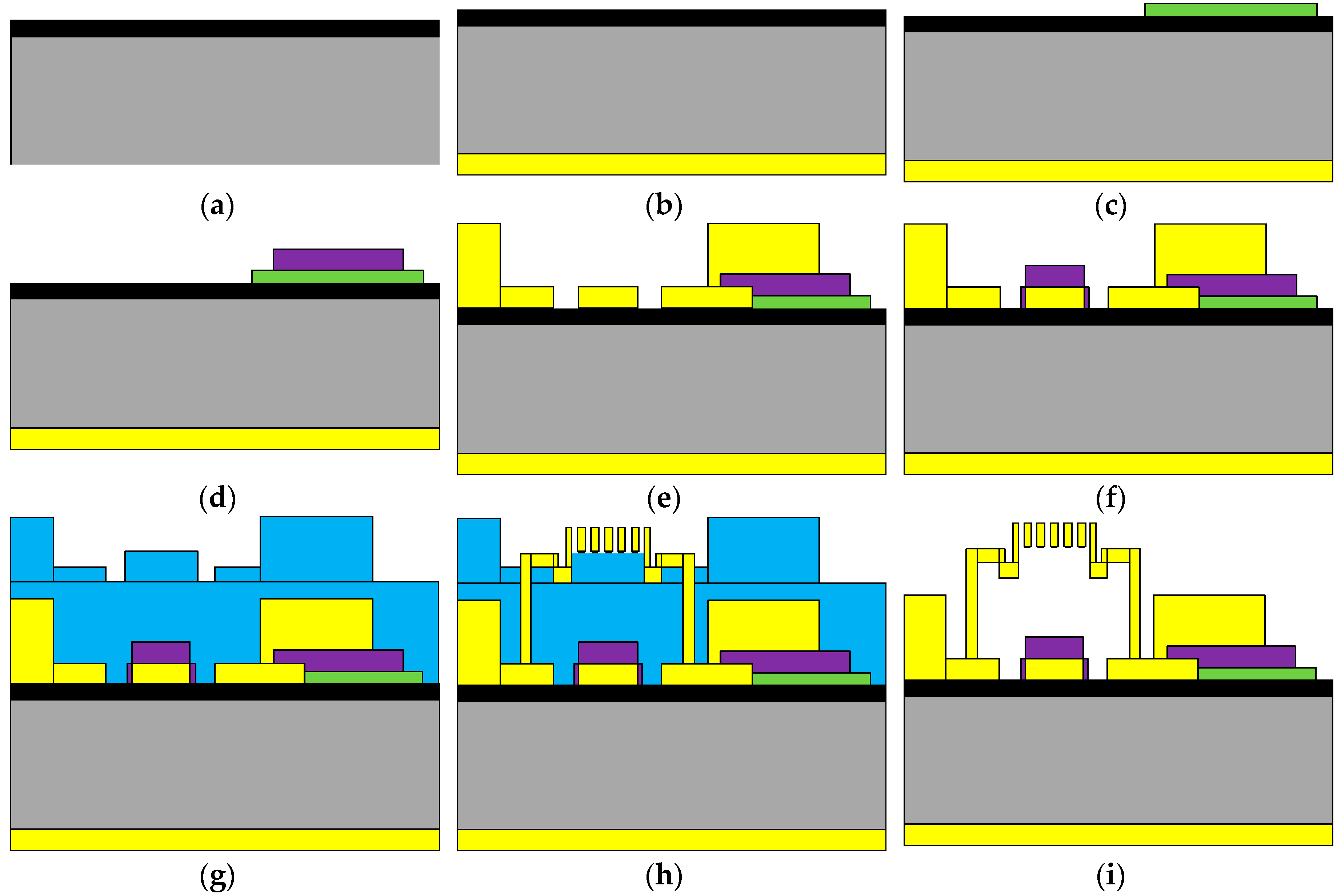
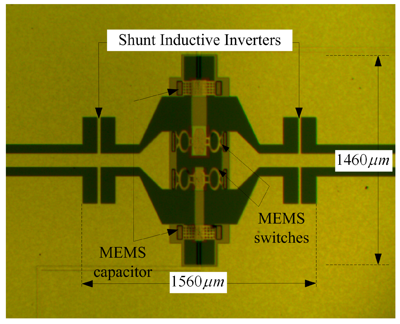
2.4. Fabrication
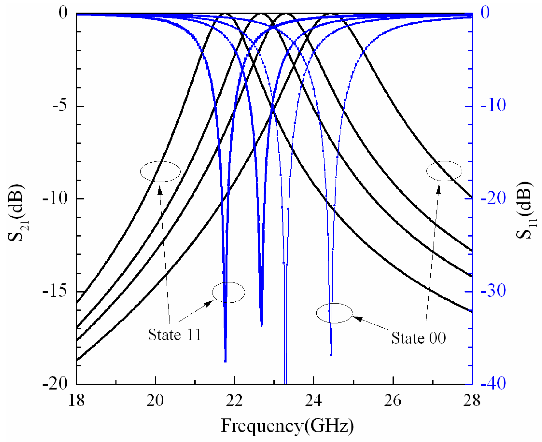
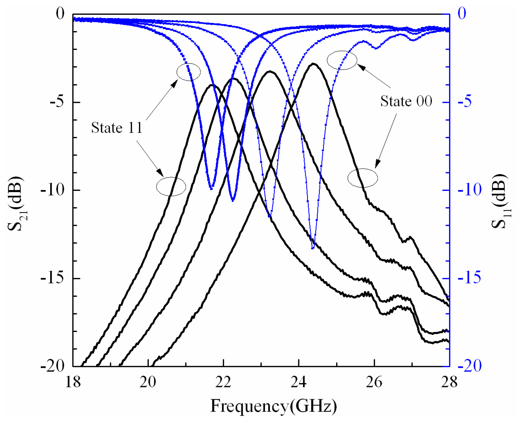
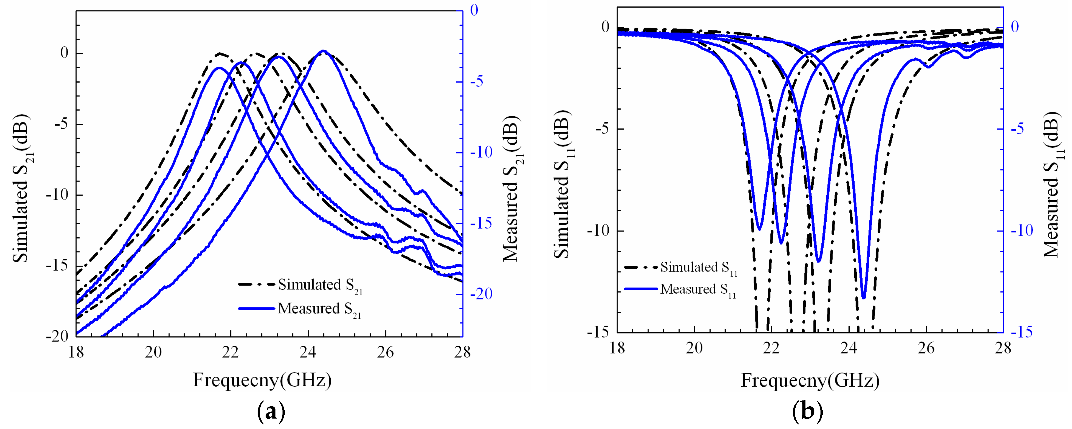
3. Measured Results and Discussion
4. Conclusions
Acknowledgments
Author Contributions
Conflicts of Interest
References
- Lee, B.; Nam, S.; Koh, B.; Kwak, C.; Lee, J. K-band frequency tunable substrate-integrated-waveguide resonator filter with enhanced stopband attenuation. IEEE Trans. Microw. Theory Tech. 2015, 63, 3632–3640. [Google Scholar] [CrossRef]
- Arnold, C.; Parlebas, J.; Zwick, T. Reconfigurable waveguide filter with variable bandwidth and center frequency. IEEE Trans. Microw. Theory Tech. 2014, 62, 1663–1670. [Google Scholar] [CrossRef]
- Yassini, B.; Yu, M.; Keats, B. A Ka-band fully tunable cavity filter. IEEE Trans. Microw. Theory Tech. 2012, 60, 4002–4012. [Google Scholar] [CrossRef]
- Pelliccia, L.; Cacciamani, F.; Sorrentino, R.; Farinelli, P.; Ligander, P.; Persson, O. High-Q MEMS-tunable waveguide filters in K-band. In Proceedings of the 42nd European Microwave Conference (EuMC), Amsterdam, The Netherlands, 29 October–1 November 2012; pp. 273–276.
- Rohrdantz, B.; Schmidt, V.; Jacob, A.F. Microstrip ring resonator based frequency reconfigurable band-pass filters at K-band. In Proceedings of the 20th International Conference on Microwaves, Radar, and Wireless Communication (MIKON), Gdansk, Poland, 16–18 June 2014; pp. 1–4.
- Subramanyam, G.; Van Keuls, F.; Miranda, F.A. A K-band tunable microstrip bandpass filter using a thin-film conductor/ferroelectric/dielectric multilayer configuration. IEEE Microw. Guided Wave Lett. 1998, 8, 78–80. [Google Scholar] [CrossRef]
- Park, J.H.; Kim, H.T.; Kwon, Y.; Kim, Y.K. Tunable millimeter-wave filters using a coplanar waveguide and micromachined variable capacitors. J. Micromech. Microeng. 2001, 11, 706–712. [Google Scholar] [CrossRef]
- Abbaspour-Tamijani, A.; Dussopt, L.; Rebeiz, G.M. A millimeter-wave tunable filter using MEMS varactors. In Proceedings of the 32nd European Microwave Conference, Milan, Italy, 23–26 September 2002; pp. 1–3.
- Abbaspour-Tamijani, A.; Dussopt, L.; Rebeiz, G.M. Miniature and tunable filters using MEMS capacitors. IEEE Trans. Microw. Theory Tech. 2003, 51, 1878–1885. [Google Scholar] [CrossRef]
- Kim, J.M.; Lee, S.; Park, J.H.; Kim, J.M.; Baek, C.W.; Kwon, Y.; Kim, Y.K. Low loss K-band tunable bandpass filter using micromachined variable capacitors. In Proceedings of the 13th International Conference on Solid-State Sensors, Actuators and Microsystems (TRANSDUCERS ’05), Seoul, Korea, 5–9 June 2005; pp. 1071–1074.
- Rebeiz, G.M. RF MEMS: Theory, Design, and Technology; Wiley: New York, NY, USA, 2003. [Google Scholar]
- Entesari, K.; Rebeiz, G.M. A 12-18-GHz Three-Pole RF MEMS Tunable Filter. IEEE Trans. Microw. Theory Tech. 2005, 53, 2566–2571. [Google Scholar] [CrossRef]
- Kaynak, M.; Wietstruck, M.; Zhang, W.; Drews, J.; Barth, R.; Knoll, D.; Korndörfer, F.; Scholz, R.; Schulz, K.; Wipf, C.; et al. Packaged BiCMOS embedded RF-MEMS switches with integrated inductive loads. In Proceedings of the IEEE MTT-S International Microwave Symposium Digest (MTT), Montreal, QC, Canada, 17–22 June 2012; pp. 1–3.
- Deng, Z.L.; Wei, H.; Fan, S.; Gan, J. Design and analysis a novel RF MEMS switched capacitor for low pull-in voltage application. Microsyst. Technol. 2016, 22, 2141–2149. [Google Scholar] [CrossRef]
- Simons, R.N. Coplanar Waveguide Circuits, Components, and Systems; John Wiley & Sons: Malden, MA, USA, 2004. [Google Scholar]
- Entesari, K.; Rebeiz, G.M. A differential 4-bit 6.5-10-GHz RF MEMS tunable filter. IEEE Trans. Microw. Theory Tech. 2005, 53, 1103–1110. [Google Scholar] [CrossRef]
- Getsinger, W.J. Circuit Duals on Planar Transmission Media. In Proceedings of the IEEE MTT-S International Microwave Symposium Digest, Boston, MA, USA, 31 May–3 June 1983; pp. 154–156.
- Beilenhoff, K.; Klingbeil, H.; Heinrich, W.; Hartnagel, H.L. Open and short circuits in coplanar MMIC’s. IEEE Trans. Microw. Theory Tech. 1993, 41, 1534–1537. [Google Scholar] [CrossRef]
- Ghione, G.; Naldi, C. Parameters of coplanar waveguides with lower ground plane. Electron. Lett. 1983, 19, 734–735. [Google Scholar] [CrossRef]
- Pozar, D.M. Microwave Engineering; John Wiley & Sons: Malden, MA, USA, 2009. [Google Scholar]
- Muldavin, J.B.; Rebeiz, G.M. High-isolation CPW MEMS shunt switches. 1. Modeling. IEEE Trans. Microw. Theory Tech. 2000, 48, 1045–1052. [Google Scholar] [CrossRef]
- Badia, M.F.B.; Buitrago, E.; Ionescu, A.M. RF MEMS shunt capacitive switches using AlN compared to dielectric. J. Microelectromech. Syst. 2012, 21, 1229–1240. [Google Scholar] [CrossRef]


© 2016 by the authors. Licensee MDPI, Basel, Switzerland. This article is an open access article distributed under the terms and conditions of the Creative Commons Attribution (CC-BY) license ( http://creativecommons.org/licenses/by/4.0/).
Share and Cite
Deng, Z.; Wei, H.; Guo, X. 21.69–24.36 GHz MEMS Tunable Band-Pass Filter. Micromachines 2016, 7, 149. https://doi.org/10.3390/mi7090149
Deng Z, Wei H, Guo X. 21.69–24.36 GHz MEMS Tunable Band-Pass Filter. Micromachines. 2016; 7(9):149. https://doi.org/10.3390/mi7090149
Chicago/Turabian StyleDeng, Zhongliang, Hao Wei, and Xubing Guo. 2016. "21.69–24.36 GHz MEMS Tunable Band-Pass Filter" Micromachines 7, no. 9: 149. https://doi.org/10.3390/mi7090149