1. Introduction
Thick polymer layers patterned by lithography have emerged as important materials in microfluidics. The most common of these materials is the epoxy polymer SU-8 that has been used to make separation systems, microreactors, valves, microneedles, polymerase chain reaction (PCR) chips, cell growth substrates and other microfluidic and biomedical microelectromechanical systems (BioMEMS) devices [
1,
2,
3]. Thicknesses of SU-8 range from sub-micrometer to hundreds of micrometers. SU-8 is easily bondable to itself [
4], making it easy to fabricate devices that are completely made of SU-8, which is important for applications where surface charge or adsorptions are important. SU-8 is a negative resist which is exposed with wavelength of 365 nm typically in 1× mask aligner.
Laser direct writing (LDW) of thick photostructurable polymers is emerging as an interesting new technology for microfabrication [
5] but there are still only few articles published on this topic. In [
6] Cadarso
et al. used LDW technique for patterning an 85 µm thick layer of an in-house epoxy-resist (EpoDWL) similar to SU-8. In this work, we are patterning the hybrid material ORMOCOMP
®. ORMOCOMP
® belongs to a class of hybrid polymers knows as Organically Modified Ceramics (Ormocers), which share beneficial material properties of polymers and ceramics [
6,
7,
8,
9]. The material was developed by Fraunhofer Institut fur Silicatforschung ISC, Wurzburg, Germany. Polymer-like behavior enables for example spin coating and patterning by UV-embossing but it has problems in residual layer that prevents the fabrication of many microstructures [
10]. ORMOCOMP
® channels have been shown to be free of fouling, as evidenced by stable migration times, which indicate that there are no hydrophobic or electrostatic interactions between ORMOCOMP
® and positively charged proteins [
11,
12].
ORMOCOMP
® has been utilized in cell growth platforms, by 3D two-photon polymerization [
7,
8,
9]. This method is in some ways similar to the one described in this work. Two-photon laser writing allows for the creation of 3D patterns of arbitrary shape (e.g., scaffolds) with sub-micrometer feature size, but is severely constrained in terms of speed compared to the method described in this work: patterning a volume of about 1000 µm
3 takes 10 min [
9], while in the same time our method can pattern a volume that is 10
6 times larger, even at the lowest patterning speed. The speed difference is mostly attributed to the fact that our method exposes a much larger volume of ORMOCOMP
® compared to two-photon laser writing.
Benefits of ORMOCOMP
®, in comparison to other lithographically patternable microfabrication polymers, are manifold: (i) adaptable elasticity modulus range (0.05 GPa to 2.35 GPa); (ii) low polymerization shrinkage of just 4.0%–5.8% by volume; (iii) solvent-free composition; (iv) thermal stability (cured ORMOCER
® material tolerates temperatures up to 300 °C); (v) oxide-like surface chemistry when cured; (vi) self-adhesive bonding; and vii) ORMOCER
® processing is simple and fast because it is solvent free—bake and developer times are just a few minutes compared with tens of minutes for photoresists of similar thickness. Due to its low shrinkage during curing, ORMOCOMP
® is very well suited for the replication of small features [
10]. In addition, nanoscale pores can be formed in ORMOCOMP
® though the use of oxygen plasma [
11]. The organic component is selectively removed, leaving an oxide skeleton with 10–100 nm pores.
In this work we show how the hybrid polymer ORMOCOMP
® is patterned by laser direct writing (LDW). In our earlier work [
12], we showed that laser direct writing can produce sharply defined structures in thick ORMOCOMP
®. In this work we explore the process conditions in detail. Maskless methods, such as laser direct writing, are ideal for prototyping new device designs. ORMOCOMP
® resembles SU-8 in being a negative resist, and it can be exposed with the same tools as SU-8. However, the need for laser patterning emerges because standard lithography of ORMOCOMP
® is limited by the fact that ORMOCOMP
® is still in liquid phase after baking. This means that proximity lithography must be employed: a very precise proximity gap control is required, otherwise mask-resist contact will tarnish the mask with liquid ORMOCOMP
® and patterns will be distorted. Using a larger proximity gap is not an option as it leads to lower resolution. LDW eliminates mask contamination, allows high resolution and high aspect ratio structures.
As applications of ORMOCOMP® patterning, we fabricated a microfluidic diode and an electrophoresis chip. The self-adhesive property of ORMOCOMP® was used to cap the electrophoresis chip. We have explored LDW parameters, using different thicknesses of ORMOCOMP® and optimized the LDW parameters to obtain the microstructures down to micrometer range, with aspect ratios of 5:1.
2. Experimental Section
2.1. Substrate Preparation
Standard silicon wafers of <100> orientation were kept in oven at 120 °C for 1 h to 2 h to dehydrate the surface.
2.2. Spin Coating
In this work, commercially available ORMOCER material ORMOCOMP® from Micro resist Technology GmbH was used. ORMOCOMP® has a high viscosity compared to most photoresists (2 ± 1 Pa·s at 25 °C). ORMOCOMP® was spin coated on the silicon wafer using different spin speeds ranging from 2000 rpm to 10,000 rpm. In addition, ORMOCOMP® shows good adhesion on most of the substrates, e.g., polymers, glasses, and silicon, without any promoters.
2.3. Pre-Baking
After spin coating the wafers were soft baked, exposed by laser, hard baked, developed and cured as shown in the flow chart in
Figure 1. Soft bake was done at 95 °C for 2 min on a hot plate. This step improves adhesion and removes any remaining air bubbles. ORMOCOMP
® was sticky after the pre bake, so it is necessary to handle the substrate carefully while mounting inside on the sample holder of laser writer. A dummy wafer was always placed under the silicon wafer because of sticky nature of uncured ORMOCOMP
®.
2.4. Laser Writing
Laser writing was done by a Microtech® (Cheshire, CT, USA) LW 405 laser writer. Design data is input using Caltech Intermediate Form (CIF) files created with suitable CAD software. The typical CIF file size for a mask design containing 100,000 polygons is roughly 5 MB.
Figure 1.
Process flow for ORMOCOMP® microstructure patterning through direct laser writing.
Figure 1.
Process flow for ORMOCOMP® microstructure patterning through direct laser writing.
The writer uses a 405 nm wavelength pulsed GaN laser, working at 8 MHz repetition rate. The pulse duration varies between 5 and 100 ns; pulse-width modulation (PWM) is used to adjust the output power of the laser source. The parameter used to set the output power of the laser source is called, by the laser writer’s user interface, Gain, and it is given in arbitrary units from 0 to 50. The nominal maximum output power is 60 mW.
The optical system has four different lenses available. These lenses allow the user to select between 1, 2, 4, and 8 µm beam waists (spot diameter at focal distance) and thus define the patterning resolution. The optical system also includes an optical filter, which can be selected for 1%, 3%, 10%, 30% and 100% of laser beam energy transfer. The sample is mounted on a XYZ stage, which comprises a vacuum chuck, and moves the sample during patterning while the laser is static. Three interconnected computer nodes control the XYZ stage, the laser source and the user interface.
The patterning can be performed in two modes: stage scan and beam scan. In stage scan, the stage moves at the same speed in the
X and
Y directions, and the laser beam is turned on and off depending on whether a given pixel needs to be exposed or not. Beam scan is similar, except that the movement in the
X-axis happens in steps that are multiples of 100, 200, 400 or 800 µm, for the lenses producing 1, 2, 4, and 8 µm spot diameters, respectively. The beam itself is scanned in the
X direction with a fast-oscillating mirror. Thus, in beam scan mode, the whole pattern is composed of 100, 200, 400, or 800 µm wide strips (
Figure 2). The scan lines overlap to a smaller or larger extent. With larger overlap, the patterned lines in the
Y direction will be smoother, and the effective dose (deposited energy per unit area) will be higher. The laser writer’s user interface allows for adjustment of the overlap. It is important to note that the beam is pulsed, and since the pulse duration is on the nanosecond scale (between 5 and 100 ns), in a first approximation the spot obtained can be considered circular,
i.e., it is not smeared into an ellipse.
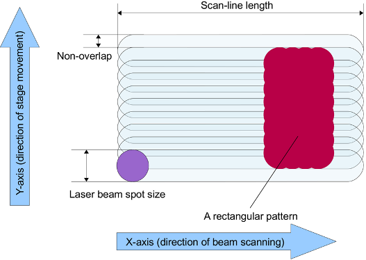
Figure 2.
A schematic illustration of the concepts of scan line, non-overlap and spot size. A patterned rectangle is shown with wavy edges. The waviness in the Y-direction is caused by finite non-overlap, whereas the waviness in the X-direction is caused by the pulsed nature of the laser beam. The exact pulse duration is not known but it is assumed to be very short, so the spot produced is not smeared into an ellipse. In this image, the non-overlap is 40%.
The intensity of the beam can be precisely adjusted, and the final dose depends on this intensity as well as the overlap of the laser beam scan lines. The selected optical filter value together with the gain parameter, define the beam intensity I as a product of Gain (a.u.) and Filter (%). Different process parameters, i.e., choice of lens, overlap, filter and gain were used to optimize exposure for different thicknesses of ORMOCOMP®.
The effective dose produced by the laser writer was determined by using a built-in optical sensor, and by measuring the time that it takes to pattern a strip of a pre-determined length with a given spot size and overlap.
2.5. Post-Baking
Post bake after laser exposure was done at 95 °C for 5 min to increase the adhesion of the replicated structures. For development of patterned microstructures, Ormodev was used. A thermal curing step of 150 °C for 1–4 h on a hotplate or oven completes the cross-linking of the molecules and hardening of the ORMOCOMP® material.
2.6. Directional Wetting Test Structure
The ORMOCOMP® directional wetting chips were treated before contact angle measurements through plasma using a microwave plasma reactor (Plasma System 400, PVA Tepla AG, Wettenberg, Germany). The microwave power was 500 W, the oxygen flow was 800 mL·min−1 and the treatment time was 10 min. Contact angle measurements were done immediately after plasma treatment using contact angle goniometer (THETA, Biolin Scientific, Stockholm, Sweden).
The directional wetting experiments were performed by depositing a large (~50 µL) droplet of de-ionized water on reservoir areas that were in contact with the directional wetting test structures. After depositing, we waited for 10 min for the liquid flow to reach its mechanical equilibrium, after which the results were analyzed by optical microscopy.
2.7. Electrophoresis Chip
Electrophoresis chips made of ORMOCOMP® have standard cross geometry (4 cm separation length) and channel dimensions (50 µm wide, 20 µm deep). A computer-controlled high voltage power supply (Microfluidic Toolkit, Micralyne, Inc., Edmonton, AB, Canada) was used for application of the potential differences. The detection was performed by laser-induced fluorescence (λex = 488 nm/20 mW) on a Leica DMIL inverted epifluorescence microscope (Leica Nilomark, Espoo, Finland) equipped with an N PLAN L 20×/0.40 c NA (numerical aperture) objective. The fluorescence emission (λem = 515–700 nm) was collected perpendicular to the microchip through a long-pass 515 nm filter on a Hamamatsu R5929 photomultiplier tube with integrated housing and a signal amplifier module (Cairn Research, Faversham, UK). A detection slit of 50 μm × 200 μm was defined onto the microchannel. A PicoScope 2203 AD converter and PicoLog software (Pico Technology, St. Neots, UK) were used for recording the signal acquired from the photomultiplier tube.
3. Results and Discussion
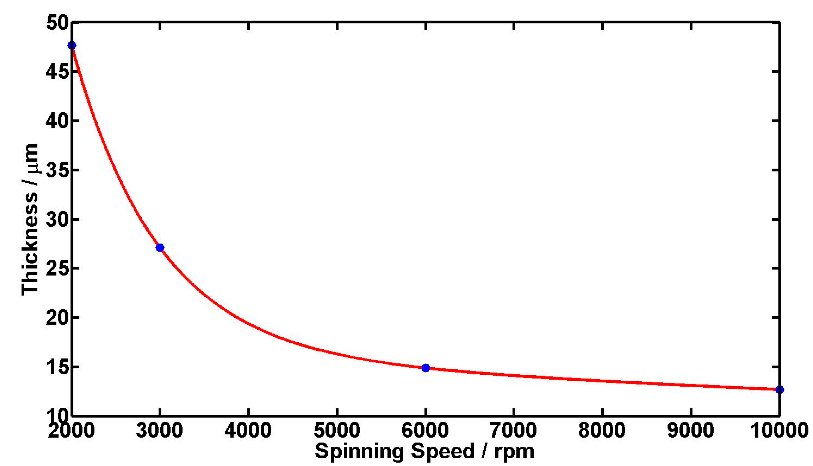
Spin coating of ORMOCOMP
® at 2000–10,000 rpm lead to film thicknesses ~50 µm down to ~10 µm. The spin curve is shown in
Figure 3. ORMOCOMP
® bake time of
ca. 2 min is very short compared with other resists of similar thickness. This is because it is solvent-free and there is no need to drive out solvents. Development times range from a few seconds to 1 min. This is again very short compared with, e.g., SU-8 where a ~50 μm layer would typically require 10–20 min.
The laser beam intensity has a Gaussian profile, and its width (or diameter of the circular spot on the substrate) is defined by the point where the intensity falls to 1/e
2 of the maximum at the center of the beam. Laser beam spot sizes of 1, 2, 4, and 8 μm were used in this work. LDW patterning time depends on the square of the spot diameter and the chosen overlap between scan lines (
Figure 2). LDW time is
ca. 90 min (in beam scan mode) for a full 100 mm wafer using the 8 μm beam spot and 6.4 µm overlap between scan lines. By increasing this overlap, the patterning speed decreases and the total effective dose increases. For instance, for the same spot size of 8 µm, increasing the overlap to 7.2 µm would double both the effective dose and the total patterning time. The doubling of the patterning time is caused by the reduction of vertical movement from 1.6 to 0.8 µm per scan-line.
Figure 3.
ORMOCOMP® layer thickness as a function of angular speed.
Figure 3.
ORMOCOMP® layer thickness as a function of angular speed.
For the further discussion of the experiments in this work, we introduce the relative non-overlap (
RNO), defined as:
The
RNO value is useful because it is dimensionless and can describe the effect of the overlap between scan-lines on overall patterning speed and effective dose in relative terms, regardless of the chosen spot size. As shown in
Figure 2, a rectangular pattern is formed with
RNO = 0.4 and the waviness of the lines is evident. Increasing
RNO would increase patterning speed but lines in the
Y-direction would be even wavier.
In early experiments both stage scan and beam scan were tried. Stage scan resulted in a too high dose (
Figure 4a) even with very low beam intensities (
Gain ~1 and
Filter = 1%). In this mode, scanning relies exclusively on the mechanical movement of the stage, the speed of which is ~1 mm·s
−1 in the
X direction and about ~100 µm·s
−1 in the
Y direction. The exact speed is unknown and it seems to be too slow for practical use. At this low scanning speed it becomes very challenging to adjust the effective dose to the low values required by ORMOCOMP
®. Due to the excessive dose produced in stage scan experiments, spaces between ridges are not resolved and ridge shapes are malformed (
Figure 4a). In beam scan mode, optimal exposure parameters could be found and microstructures were resolved successfully (
Figure 4b). Beam scan parameters were
RNO = 0.2,
Gain = 30 and
Filter = 3%, resulting in an effective dose of 1.6 J·cm
−2. All further experiments were done in beam scan mode.
Figure 5 shows images of over-exposed ~50 µm high (2000 rpm) ORMOCOMP
® ridges. Microstructures in
Figure 5a are patterned with 1 µm spot size and effective dose of 2.7 J·cm
−2. Gross over-exposure produces ~20 µm thick cured material between ridges. In
Figure 5b, we see a scenario where ORMOCOMP
® ridges are slightly overexposed. In this case, the sample was patterned with 4 µm spot size and effective dose of 1.8 J·cm
−2. In the case of slight over-exposure, the light reflected from the substrate and refracted by already exposed ORMOCOMP
® causes an uneven distribution of cured material between ridges.
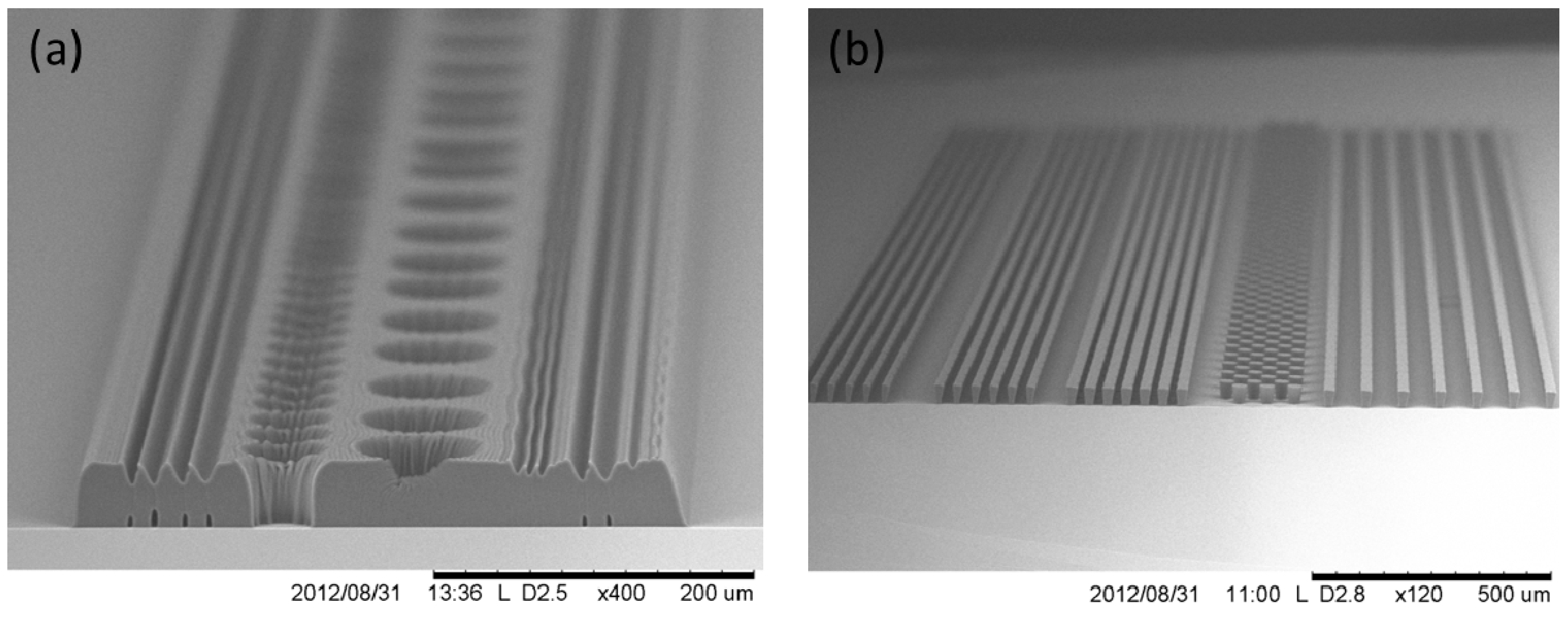
Figure 4.
SEM(scanning electron microscope) images of ~50 µm thick (spinned at 2000 rpm) laser-patterned ORMOCOMP® using 1 µm spot size and two different scan modes: (a) Stage scan with an estimated dose of ~10 J·cm−2; (b) Beam scan with an effective dose of 1.6 J·cm−2.
Figure 4.
SEM(scanning electron microscope) images of ~50 µm thick (spinned at 2000 rpm) laser-patterned ORMOCOMP® using 1 µm spot size and two different scan modes: (a) Stage scan with an estimated dose of ~10 J·cm−2; (b) Beam scan with an effective dose of 1.6 J·cm−2.
Figure 5.
Over-exposed ORMOCOMP® microstructures of ~40 µm height at 2000 rpm: (a) 1 µm spot size and effective dose of 2.7 J·cm−2; and (b) 4 µm spot size and effective dose of 1.8 J·cm−2.
Figure 5.
Over-exposed ORMOCOMP® microstructures of ~40 µm height at 2000 rpm: (a) 1 µm spot size and effective dose of 2.7 J·cm−2; and (b) 4 µm spot size and effective dose of 1.8 J·cm−2.
The exposure parameters that can be modified to achieve well-defined structures are the Filter, Gain and RNO. All of these parameters have to be optimized separately for each of the four spot sizes and different ORMOCOMP® thickness. To simplify the task, the same non-overlap RNO = 0.2 was selected and used for all four spot sizes. The choice RNO = 0.2 for this overlap is based on engineering judgment of patterning speed and smoothness of sidewalls in the Y direction.
We performed the following experiment: the laser writer’s built-in optical sensor measured the laser power immediately before the optics, and the obtained value was
P = 57.7 mW, slightly less than the nominal value of 60 mW. Using this value and the time necessary to pattern a single 20 mm long strip with overlap factor
RNO = 0.2, we derived the effective dose values in
Table 1. To obtain the values in
Table 1, we assumed that the whole power
P = 57.7 mW is uniformly distributed over the area of a 20 mm long strip (for a 1 µm spot diameter, the area is
A = 20 mm × 100 µm = 2 mm
2). This way we have the area, the power and the time duration of exposure, which gives the dose in J·cm
−2. These values relate to
Filter = 100% and
Gain = 50 (maximum gain in arbitrary units). The actual dose used for a given combination of
Filter and
Gain is obtained by multiplying the values in
Table 1 by the filter and relative gain (
Gain/50). For instance, the pillars (~50 µm high) in
Figure 6a were obtained with a spot size of 4 µm,
Gain = 40 and
Filter = 30% so the effective dose used in the experiment was (40/50) × 0.3 × 6.1 J·cm
−2 = 1.46 J·cm
−2. For SU-8 of similar thickness standard UV-exposure doses of 300 mJ·cm
−2 would be used. However, we use a monochromatic 405 nm wavelength of the laser source, while SU-8 is sensitive at the
i-line (365 nm) of a mercury lamp, so direct comparison is not relevant. The high aspect ratio (5:1) structures in
Figure 6b were obtained with a spot size of 1 µm and the exposure parameters were
Filter = 3% and
Gain = 30 (dose 1.6 J·cm
−2), for ~50 µm tall and ~10 µm wide ridges. Round pillars with the height of ~50 μm (
Figure 6c) were made with a spot size of 1 µm and exposure parameters
Filter = 1% and
Gain = 45 (dose 0.81 J·cm
−2). In
Figure 6d, ORMOCOMP
® triangles with 30°, 45° and 90° angles are shown (~13 μm high, 10,000 rpm). The spot size used was 2 µm,
Filter = 10% and
Gain = 18 (dose 0.82 J·cm
−2). The small radius of curvature of the corners, a few micrometers, indicates that LDW of ORMOCOMP
® microstructures has advantages over proximity lithography and is useful for applications requiring high definition and small line edge roughness. In proximity lithography of ORMOCOMP
® a 100 µm gap must be used because of beading of the liquid ORMOCOMP
®. In consequence, the radius of curvature of corners is of the order of minimum resolvable features ([
13], Section 9.2), which is 10–20 µm depending on layer thickness.
Table 1.
Effective dose calculated for each laser spot diameter, with non-overlap RNO = 0.2, Gain = 50 and Filter = 100%.
Table 1.
Effective dose calculated for each laser spot diameter, with non-overlap RNO = 0.2, Gain = 50 and Filter = 100%.
| Spot diameter (µm) | Effective dose for Gain = 50 & Filter = 100% (J·cm−2) |
|---|
| 1 | 93.7 |
| 2 | 23.8 |
| 4 | 6.1 |
| 8 | 1.6 |
Laser direct written epoxy (EpoDLW) patterns described in [
6] were 3–85 µm thick. If we compare our ORMOCOMP
® patterns in 40 µm thick film with those of 40 µm thick EpoDLW, our resolution of arrayed features is similar, with 1:1 and 2:1 aspect ratios typically. Both studies indicate vertical profiles with high fidelity. However, in [
6] they produced isolated lines with very high aspect ratios of 10:1 and even 40:1. Our best case was 5:1 aspect ratio. In both studies the profiles of isolated high aspect ratio structures were far from optimal and need further optimization.
Figure 6.
SEM images of optimally exposed ORMOCOMP®: (a) ~50 µm tall ridges patterned with spot size 4 µm and dose 1.46 J·cm−2; (b) ~50 µm tall and ~10 µm wide ridges patterned with 1 µm spot size and dose 1.6 J·cm−2; (c) ~50 µm high pillars patterned with spot size 1 µm and dose 0.81 J·cm−2 and (d) ~13 µm high triangles patterned with spot size 2 µm and dose 0.82 J·cm−2.

 ,
, 


