

Perovskite Solar Cells: A Review of the Latest Advances in Materials, Fabrication Techniques, and Stability Enhancement Strategies


Abstract
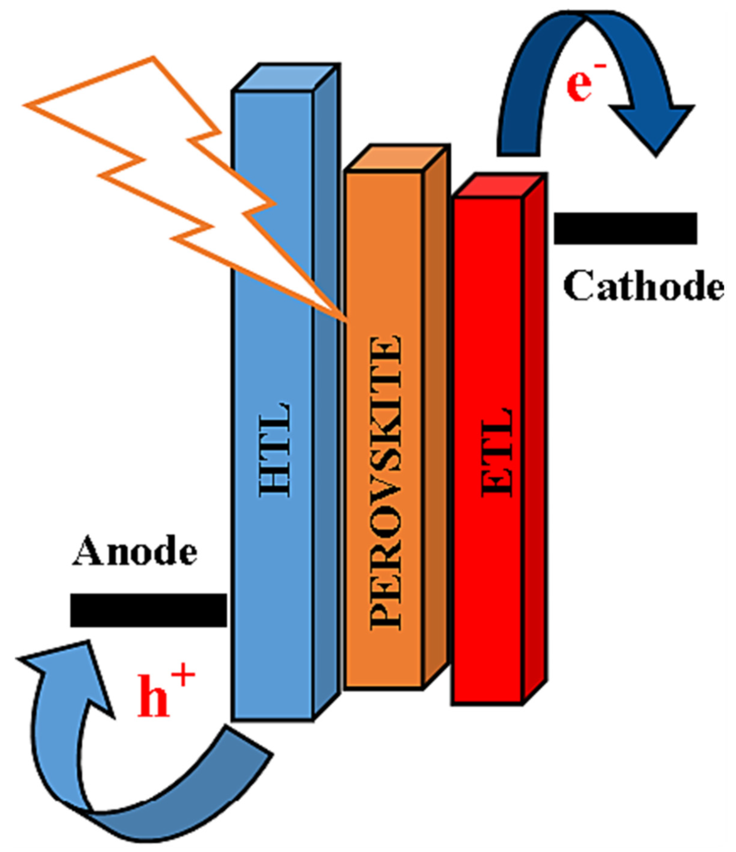
:1. Introduction
- (i)
- Stability: PSCs’ performance and lifespan can be negatively impacted by exposure to moisture, oxygen, light, heat, and mechanical stress. The primary causes of PSC instability are the interfacial reactions between the perovskite and CTLs, the intrinsic instability of the perovskite materials, and the deterioration of the electrodes and encapsulation materials [11];
- (ii)
- Scalability: PSCs are primarily made using solution-based techniques like inkjet printing and spin coating, which work well for small-area devices but not for large-area modules. Therefore, the development of scalable fabrication techniques that can produce high-quality, uniform perovskite films and devices over large areas is required. Examples of these techniques include roll-to-roll processing, doctor blading, slot–die coating, and spray coating;
- (iii)
- Toxicity: Lead, which is a common ingredient in PSCs, is a heavy metal that is toxic and poses major health and environmental risks. Thus, it is necessary to reduce the amount of lead by alloying it with other metals or using mixed-halide perovskites, or to replace lead with less toxic or non-toxic alternatives like tin, bismuth, or antimony.
- (i)
- Tandem cells: By varying the perovskite materials’ composition, PSCs can exhibit a band gap that is tunable. In order to harvest a wider spectrum of solar radiation and achieve higher PCE, this allows for the fabrication of tandem or multi-junction cells, where two or more PSCs with different band gaps are stacked on top of each other, or on top of a silicon or thin-film solar cell;
- (ii)
- Flexible and wearable devices: Using low-temperature and solution-based techniques, PSCs can be fabricated on flexible substrates like plastic or metal foils. This allows for the integration of PSCs with wearable electronics like smart watches, sensors, or displays, as well as the creation of flexible and lightweight solar modules for a variety of uses [12,13,14];
- (iii)
- Perovskite light-emitting diodes (LEDs) and lasers: PSCs can also function as light-emitting devices by introducing electrons and holes into the perovskite layer through an applied voltage; within this layer, electrons and holes recombine and emit light. High brightness, color purity, and tunability have been demonstrated by perovskite LEDs and lasers, which can be used for illumination, displays, or communication.
2. Materials
2.1. Perovskite Absorber Materials
2.1.1. Crystal Structure and Electronic Properties of Perovskites
2.1.2. Composition Engineering and Band Gap Tuning of Perovskites
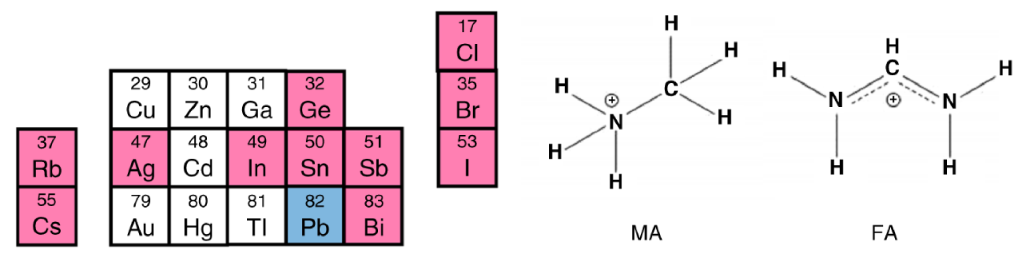
2.1.3. Lead-Free and Low-Toxicity Perovskites
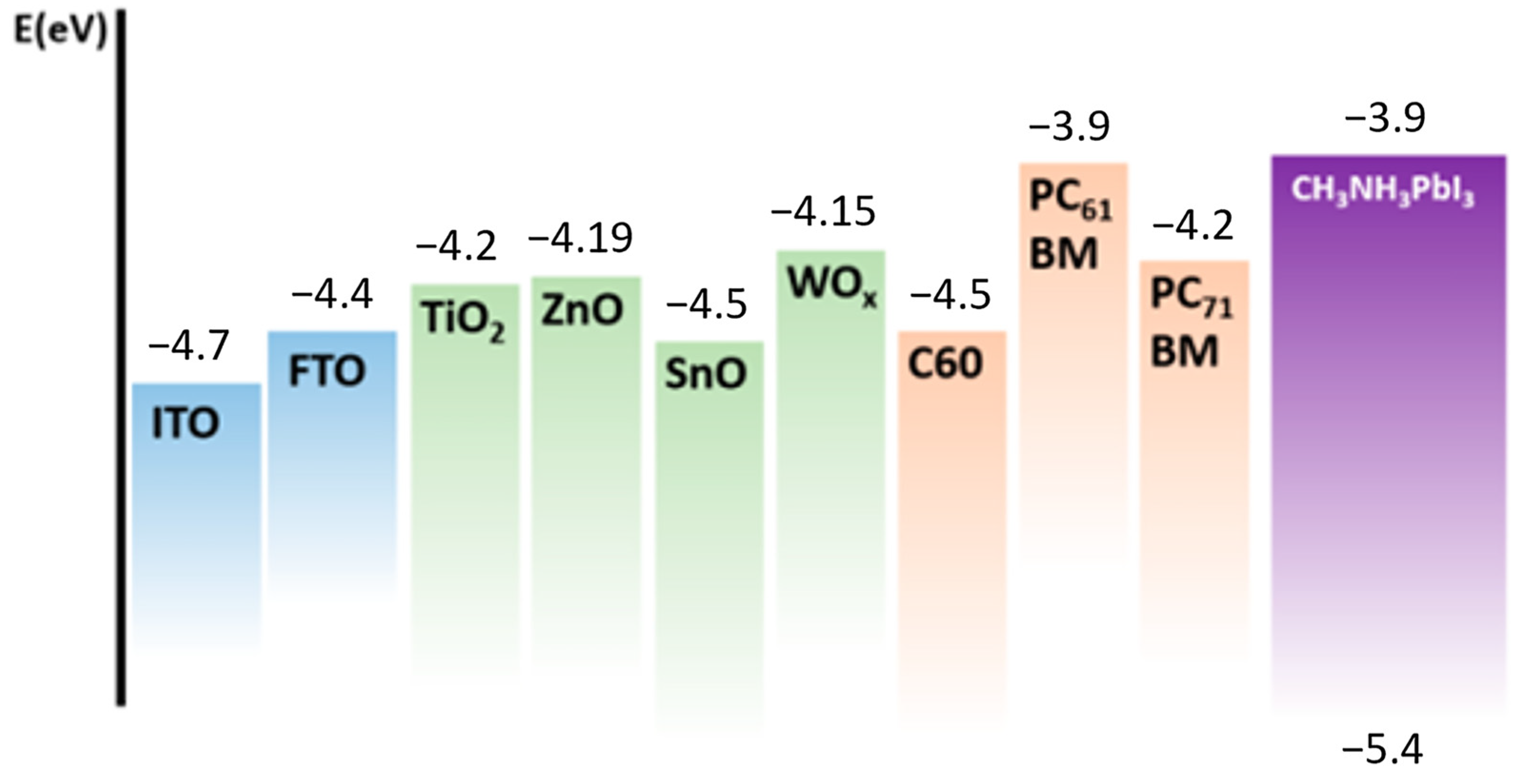
2.2. Charge Transport Materials
2.2.1. Hole Transport Materials (HTMs)
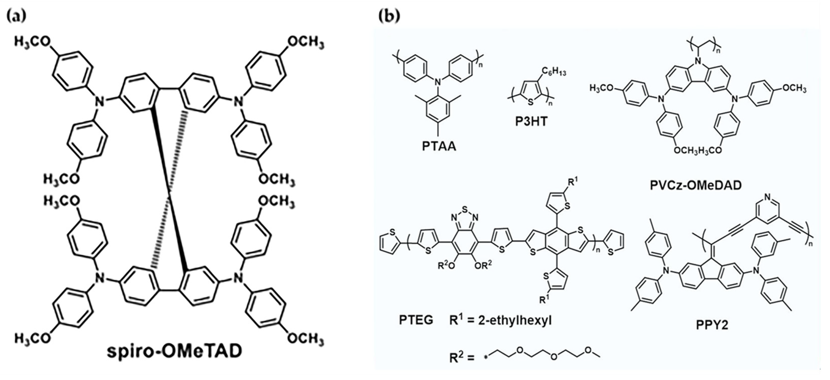
Organic HTMs
Inorganic HTMs
Carbon-Based HTMs
2.2.2. Electron Transport Materials (ETMs)
Organic ETMs
Inorganic ETMs
2.3. Electrode Materials
2.3.1. Transparent Electrodes
2.3.2. Metal Electrodes
Gold (Au)
Silver (Ag)
Other Metals and Alloys
2.3.3. Carbon Electrodes
3. Fabrication Techniques
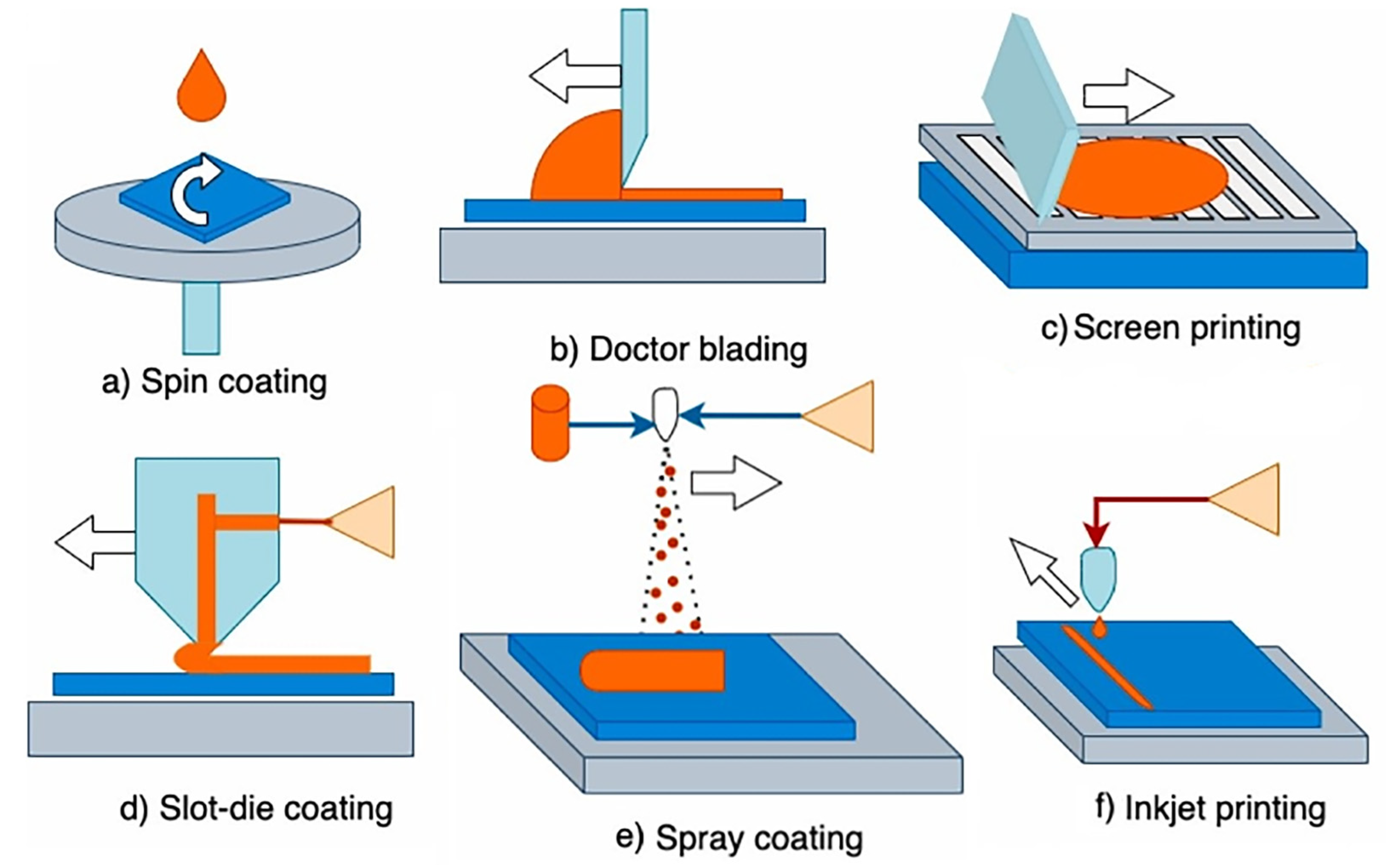
3.1. Solution-Based Techniques
3.1.1. Spin Coating
3.1.2. Doctor Blading
3.1.3. Screen Printing
3.1.4. Slot-Die Coating
3.1.5. Spray Coating
3.1.6. Inkjet Printing
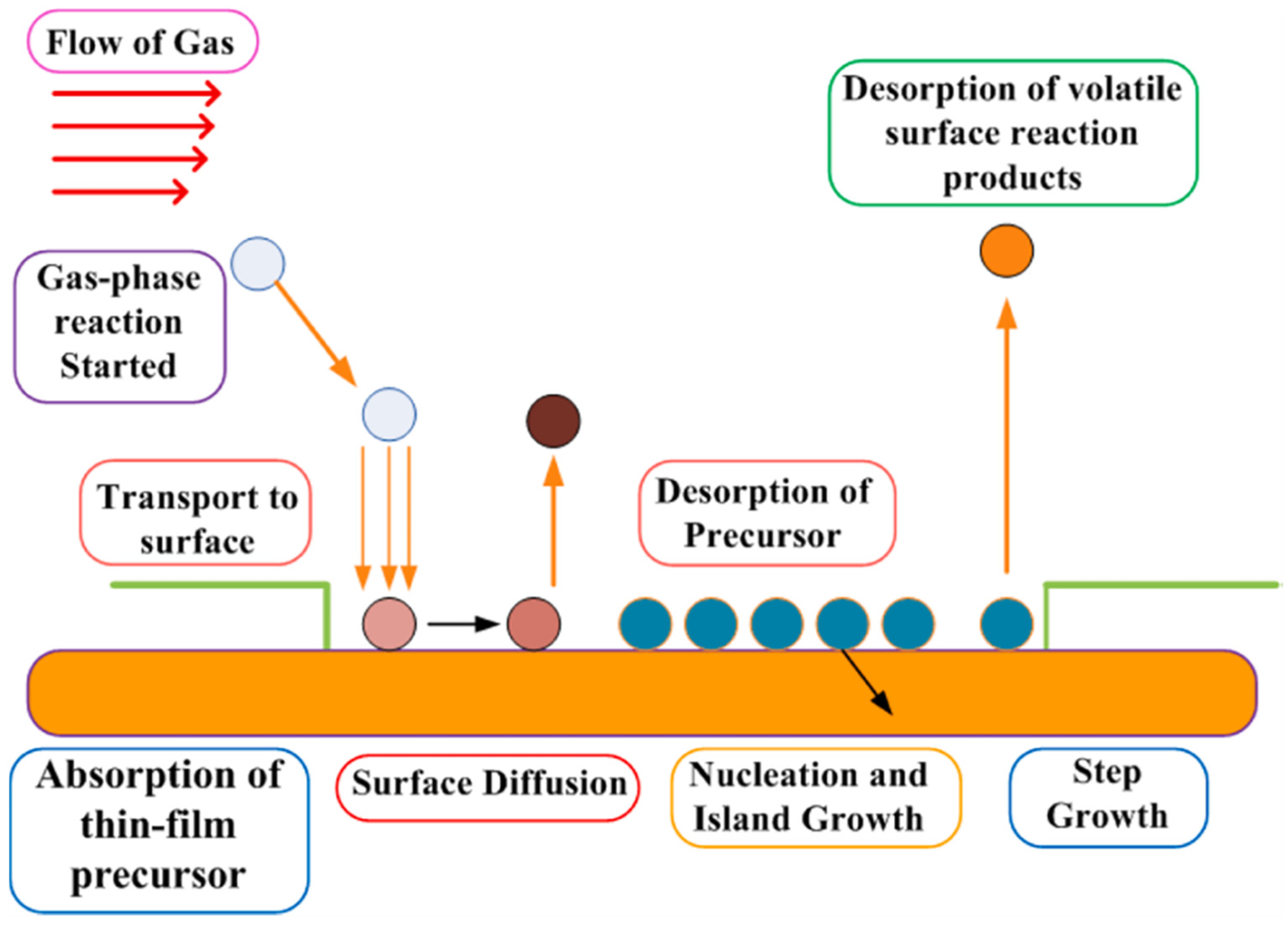
3.2. Vapor-Based Techniques
3.2.1. Physical Vapor Deposition (PVD)
3.2.2. Chemical Vapor Deposition (CVD)
3.2.3. Hybrid Vapor Deposition
3.3. Other Techniques
3.3.1. Sol-Gel Method
3.3.2. Electrodeposition
3.3.3. Laser Ablation
4. Discussion
4.1. Stability Enhancement Strategies
4.2. Materials Modification and Optimization
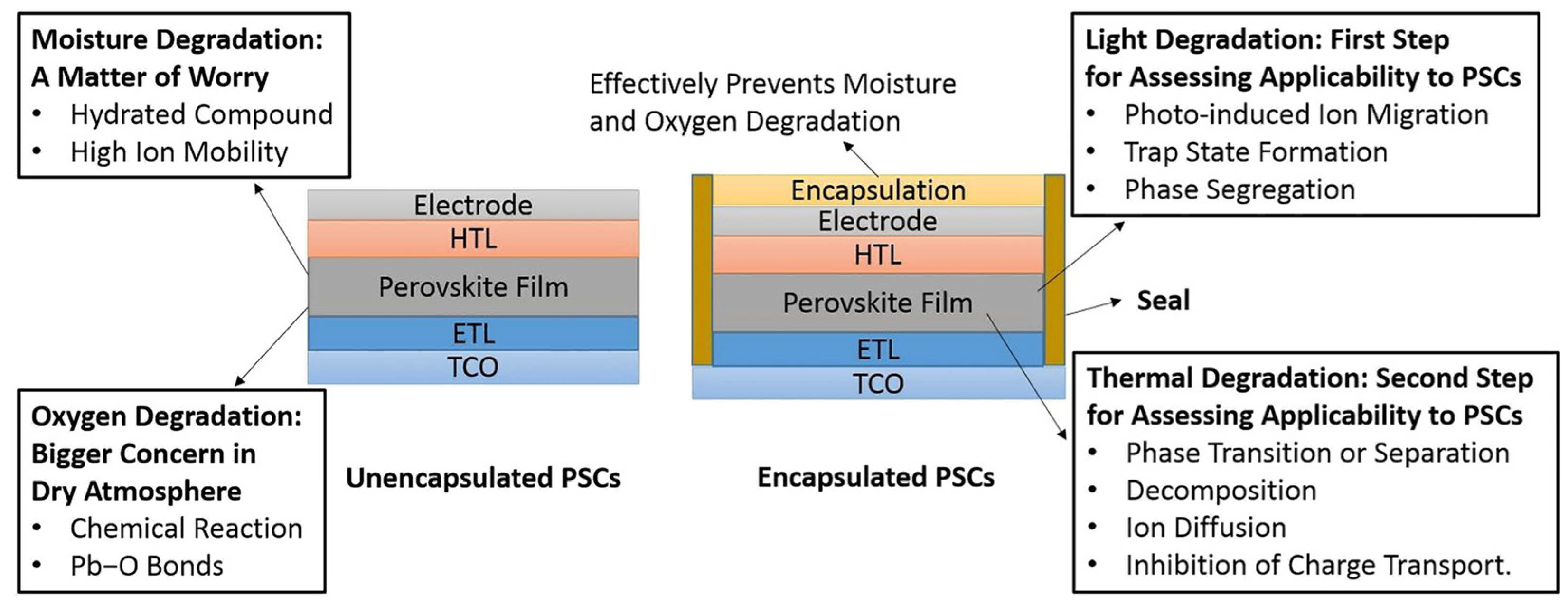
4.3. Device Encapsulation and Protection
4.3.1. Glass Encapsulation and Edge Sealing
4.3.2. Polymer Encapsulation and Coating
4.4. Environmental and Operational Factors
4.4.1. Humidity and Moisture Effects and Mitigation
4.4.2. Temperature and Thermal Effects and Mitigation
4.4.3. Light Illumination and Photodegradation Effects and Mitigation
5. Conclusions and Outlook
- -
- Developing novel and environmentally friendly perovskite materials and compositions that can achieve high efficiency, stability, and reproducibility, while avoiding the use of toxic or scarce elements.
- -
- Optimizing the device architecture and interface engineering to enhance the charge transport, extraction, and collection, as well as to reduce the parasitic losses and degradation mechanisms.
- -
- Scaling up the fabrication techniques from lab to fab, using industry-compatible and scalable methods that can produce large-area and uniform PSCs with high yield and quality.
- -
- Improving the stability of PSCs under various operating and environmental conditions, such as temperature, humidity, light, oxygen, and mechanical stress, by employing effective encapsulation and protection methods, as well as designing self-healing and adaptive PSCs.
- -
- Evaluating the environmental impact and life cycle assessment of PSCs, as well as addressing the lead toxicity and recycling issues, by following the principles of green chemistry and circular economy.
Author Contributions
Funding
Data Availability Statement
Acknowledgments
Conflicts of Interest
References
- Roy, P.; Ghosh, A.; Barclay, F.; Khare, A.; Cuce, E. Perovskite solar cells: A review of the recent advances. Coatings 2022, 12, 1089. [Google Scholar] [CrossRef]
- Sharif, R.; Khalid, A.; Ahmad, S.W.; Rehman, A.; Qutab, H.G.; Akhtar, H.H.; Mahmood, K.; Afzal, S.; Saleem, F. A comprehensive review of the current progresses and material advances in perovskite solar cells. Nanoscale Adv. 2023, 5, 3803–3833. [Google Scholar] [CrossRef]
- Zhang, P.; Li, M.; Chen, W.-C. A perspective on perovskite solar cells: Emergence, progress, and commercialization. Front. Chem. 2022, 10, 802890. [Google Scholar] [CrossRef]
- Chen, Y.; Zhang, L.; Zhang, Y.; Gao, H.; Yan, H. Large-area perovskite solar cells—A review of recent progress and issues. RSC Adv. 2018, 8, 10489–10508. [Google Scholar] [CrossRef] [PubMed]
- Shao, J.-Y.; Zhong, Y.-W. Design of small molecular hole-transporting materials for stable and high-performance perovskite solar cells. Chem. Phys. Rev. 2021, 2, 021302. [Google Scholar] [CrossRef]
- Anoop, K.M.; Ahipa, T.N. Recent advancements in the hole transporting layers of perovskite solar cells. Sol. Energy 2023, 263, 111937. [Google Scholar] [CrossRef]
- Desoky, M.M.H.; Bonomo, M.; Buscaino, R.; Fin, A.; Viscardi, G.; Barolo, C.; Quagliotto, P. Dopant-free all-organic small-molecule HTMS for perovskite solar cells: Concepts and structure–property relationships. Energies 2021, 14, 2279. [Google Scholar] [CrossRef]
- Jung, H.S.; Park, N.-G. Perovskite solar cells: From materials to devices. Small 2015, 11, 10–25. [Google Scholar] [CrossRef]
- Shaikh, D.B.; Wenbo, L.; Bhosale, R.S.; Said, A.A.; Kobaisi, M.A.; Bhosale, S.V.; Bhosale, S.V.; Zhang, Q. Novel core-modulated naphthalenediimides with CN-TFPA as electron transport layer for inverted perovskite solar cells. Mater. Res. Bull. 2020, 132, 111009. [Google Scholar] [CrossRef]
- Meng, L.; You, J.; Guo, T.-F.; Yang, Y. Recent advances in the inverted planar structure of perovskite solar cells. Acc. Chem. Res. 2016, 49, 155–165. [Google Scholar] [CrossRef] [PubMed]
- Wu, T.; Qin, Z.; Wang, Y.; Wu, Y.; Chen, W.; Zhang, S.; Cai, M.; Dai, S.; Zhang, J.; Liu, J.; et al. The main progress of perovskite solar cells in 2020–2021. Nano-Micro Lett. 2021, 13, 152. [Google Scholar] [CrossRef]
- Hu, Z.; Ran, C.; Zhang, H.; Chao, L.; Chen, Y.; Huang, W. The current status and development trend of perovskite solar cells. Engineering 2023, 21, 15–19. [Google Scholar] [CrossRef]
- Liu, C.; Cheng, Y.-B.; Ge, Z. Understanding of perovskite crystal growth and film formation in scalable deposition processes. Chem. Soc. Rev. 2020, 49, 1653–1687. [Google Scholar] [CrossRef]
- Yan, J.; Savenije, T.J.; Mazzarella, L.; Isabella, O. Progress and challenges on scaling up of perovskite solar cell technology. Sustain. Energy Fuels 2022, 6, 243–266. [Google Scholar] [CrossRef]
- Marongiu, D.; Saba, M.; Quochi, F.; Mura, A.; Bongiovanni, G. The role of excitons in 3D and 2D lead halide perovskites. J. Mater. Chem. C 2019, 7, 12006–12018. [Google Scholar] [CrossRef]
- Li, K.; Dong, L.-Y.; Xu, H.-X.; Qin, Y.; Li, Z.-G.; Azeem, M.; Li, W.; Bu, X.-H. Electronic structures and elastic properties of a family of metal-free perovskites. Mater. Chem. Front. 2019, 3, 1678–1685. [Google Scholar] [CrossRef]
- Mirseraji, M.; Shahraki, M.G. DFT study of the polarization behaviors of various distorted barium titanate crystals: The role of atomic displacements. Phys. B 2018, 538, 120–130. [Google Scholar] [CrossRef]
- Ku, Z.; Rong, Y.; Xu, M.; Liu, T.; Han, H. Full printable processed mesoscopic CH3NH3PbI3/TiO2 heterojunction solar cells with carbon counter electrode. Sci. Rep. 2013, 3, 3132. [Google Scholar] [CrossRef]
- Zhou, R.; Yang, Z.; Xu, J.; Cao, G. Synergistic combination of semiconductor quantum dots and organic-inorganic halide perovskites for hybrid solar cells. Coord. Chem. Rev. 2018, 374, 279–313. [Google Scholar] [CrossRef]
- Zhang, X.; Turiansky, M.E.; Van de Walle, C.G. Correctly assessing defect tolerance in halide perovskites. J. Phys. Chem. C 2020, 124, 6022–6027. [Google Scholar] [CrossRef]
- Muralt, P.; Polcawich, R.G.; Trolier-McKinstry, S. Piezoelectric thin films for sensors, actuators, and energy harvesting. MRS Bull. 2009, 34, 658–664. [Google Scholar] [CrossRef]
- Bowman, A.R.; Klug, M.T.; Doherty, T.A.S.; Farrar, M.D.; Senanayak, S.P.; Wenger, B.; Divitini, G.; Booker, E.P.; Andaji-Garmaroudi, Z.; Macpherson, S.; et al. Microsecond carrier lifetimes, controlled p-doping, and enhanced air stability in low-bandgap metal halide perovskites. ACS Energy Lett. 2019, 4, 2301–2307. [Google Scholar] [CrossRef]
- Zhang, H.; Nazeeruddin, M.K.; Choy, W.C.H. Perovskite photovoltaics: The significant role of ligands in film formation, passivation, and stability. Adv. Mater. 2019, 31, 1805702. [Google Scholar] [CrossRef] [PubMed]
- Saidaminov, M.I.; Kim, J.; Jain, A.; Quintero-Bermudez, R.; Tan, H.; Long, G.; Tan, F.; Johnston, A.; Zhao, Y.; Voznyy, O.; et al. Suppression of atomic vacancies via incorporation of isovalent small ions to increase the stability of halide perovskite solar cells in ambient air. Nat. Energy 2018, 3, 648–654. [Google Scholar] [CrossRef]
- Li, Y.; Lu, Y.; Huo, X.; Wei, D.; Meng, J.; Dong, J.; Qiao, B.; Zhao, S.; Xu, Z.; Song, D. Bandgap tuning strategy by cations and halide ions of lead halide perovskites learned from machine learning. RSC Adv. 2021, 11, 15688–15694. [Google Scholar] [CrossRef] [PubMed]
- Afsari, M.; Boochani, A.; Hantezadeh, M. Electronic, optical and elastic properties of cubic perovskite CsPbI3: Using first principles study. Optik 2016, 127, 11433–11443. [Google Scholar] [CrossRef]
- Raga, S.R.; Jiang, Y.; Ono, L.K.; Qi, Y. Application of methylamine gas in fabricating organic–inorganic hybrid perovskite solar cells. Energy Technol. 2017, 5, 1750–1761. [Google Scholar] [CrossRef]
- Urieta-Mora, J.; García-Benito, I.; Molina-Ontoria, A.; Martín, N. Hole transporting materials for perovskite solar cells: A chemical approach. Chem. Soc. Rev. 2018, 47, 8541–8571. [Google Scholar] [CrossRef] [PubMed]
- Xie, Y.-M.; Xue, Q.; Yip, H.-L. Metal-halide perovskite crystallization kinetics: A review of experimental and theoretical studies. Adv. Energy Mater. 2021, 11, 2100784. [Google Scholar] [CrossRef]
- Zhou, M.; Sarmiento, J.S.; Fei, C.; Zhang, X.; Wang, H. Effect of composition on the spin relaxation of lead halide perovskites. J. Phys. Chem. Lett. 2020, 11, 1502–1507. [Google Scholar] [CrossRef]
- Sarkar, D.; Hooper, R.W.; Karmakar, A.; Bhattacharya, A.; Pominov, A.; Terskikh, V.V.; Michaelis, V.K. Metal halide perovskite and perovskite-like materials through the lens of ultra-wideline 35/37Cl NMR spectroscopy. ACS Mater. Lett. 2022, 4, 1255–1263. [Google Scholar] [CrossRef]
- Ou, Q.; Bao, X.; Zhang, Y.; Shao, H.; Xing, G.; Li, X.; Shao, L.; Bao, Q. Band structure engineering in metal halide perovskite nanostructures for optoelectronic applications. Nano Mater. Sci. 2019, 1, 268–287. [Google Scholar] [CrossRef]
- Braly, I.L.; Stoddard, R.J.; Rajagopal, A.; Uhl, A.R.; Katahara, J.K.; Jen, A.K.-Y.; Hillhouse, H.W. Current-induced phase segregation in mixed halide hybrid perovskites and its impact on two-terminal tandem solar cell design. ACS Energy Lett. 2017, 2, 1841–1847. [Google Scholar] [CrossRef]
- DeQuilettes, D.W.; Zhang, W.; Burlakov, V.M.; Graham, D.J.; Leijtens, T.; Osherov, A.; Bulović, V.; Snaith, H.J.; Ginger, D.S.; Stranks, S.D. Photo-induced halide redistribution in organic–inorganic perovskite films. Nat. Commun. 2016, 7, 11683. [Google Scholar] [CrossRef]
- Noel, N.K.; Stranks, S.D.; Abate, A.; Wehrenfennig, C.; Guarnera, S.; Haghighirad, A.-A.; Sadhanala, A.; Eperon, G.E.; Pathak, S.K.; Johnston, M.B.; et al. Lead-free organic–inorganic tin halide perovskites for photovoltaic applications. Energy Environ. Sci. 2014, 7, 3061–3068. [Google Scholar] [CrossRef]
- Li, Y.; Song, D.; Meng, J.; Dong, J.; Lu, Y.; Huo, X.; Maqsood, A.; Song, Y.; Zhao, S.; Qiao, B.; et al. Solvent modification to suppress halide segregation in mixed halide perovskite solar cells. J. Mater. Sci. 2020, 55, 9787–9794. [Google Scholar] [CrossRef]
- Li, N.; Tao, S.; Chen, Y.; Niu, X.; Onwudinanti, C.K.; Hu, C.; Qiu, Z.; Xu, Z.; Zheng, G.; Wang, L.; et al. Cation and anion immobilization through chemical bonding enhancement with fluorides for stable halide perovskite solar cells. Nat. Energy 2019, 4, 408–415. [Google Scholar] [CrossRef]
- Shai, X.; Wang, J.; Sun, P.; Huang, W.; Liao, P.; Cheng, F.; Zhu, B.; Chang, S.-Y.; Yao, E.-P.; Shen, Y.; et al. Achieving ordered and stable binary metal perovskite via strain engineering. Nano Energy 2018, 48, 117–127. [Google Scholar] [CrossRef]
- Wang, Z.; Zhu, X.; Zuo, S.; Chen, M.; Zhang, C.; Wang, C.; Ren, X.; Yang, Z.; Liu, Z.; Xu, X.; et al. 27%-efficiency four-terminal perovskite/silicon tandem solar cells by sandwiched gold nanomesh. Adv. Funct. Mater. 2020, 30, 1908298. [Google Scholar] [CrossRef]
- Futscher, M.H.; Ehrler, B. Efficiency limit of perovskite/Si tandem solar cells. ACS Energy Lett. 2016, 1, 863–868. [Google Scholar] [CrossRef]
- Yu, Z.J.; Carpenter, J.V., III; Holman, Z.C. Techno-economic viability of silicon-based tandem photovoltaic modules in the United States. Nat. Energy 2018, 3, 747–753. [Google Scholar] [CrossRef]
- Li, Z.; Zhao, Y.; Wang, X.; Sun, Y.; Zhao, Z.; Li, Y.; Zhou, H.; Chen, Q. Cost analysis of perovskite tandem photovoltaics. Joule 2018, 2, 1559–1572. [Google Scholar] [CrossRef]
- Hoke, E.T.; Slotcavage, D.J.; Dohner, E.R.; Bowring, A.R.; Karunadasa, H.I.; McGehee, M.D. Reversible photo-induced trap formation in mixed-halide hybrid perovskites for photovoltaics. Chem. Sci. 2015, 6, 613–617. [Google Scholar] [CrossRef] [PubMed]
- Bush, K.A.; Frohna, K.; Prasanna, R.; Beal, R.E.; Leijtens, T.; Swifter, S.A.; McGehee, M.D. Compositional engineering for efficient wide band gap perovskites with improved stability to photoinduced phase segregation. ACS Energy Lett. 2018, 3, 428–435. [Google Scholar] [CrossRef]
- Barker, A.J.; Sadhanala, A.; Deschler, F.; Gandini, M.; Senanayak, S.P.; Pearce, P.M.; Mosconi, E.; Pearson, A.J.; Wu, Y.; Srimath Kandada, A.R.; et al. Defect-assisted photoinduced halide segregation in mixed-halide perovskite thin films. ACS Energy Lett. 2017, 2, 1416–1424. [Google Scholar] [CrossRef]
- Gharibzadeh, S.; Abdollahi Nejand, B.; Jakoby, M.; Abzieher, T.; Hauschild, D.; Moghadamzadeh, S.; Schwenzer, J.A.; Brenner, P.; Schmager, R.; Haghighirad, A.A.; et al. Record open-circuit voltage wide-bandgap perovskite solar cells utilizing 2D/3D perovskite heterostructure. Adv. Energy Mater. 2019, 9, 1803699. [Google Scholar] [CrossRef]
- Wang, M.; Wang, W.; Ma, B.; Shen, W.; Liu, L.; Cao, K.; Chen, S.; Huang, W. Lead-free perovskite materials for solar cells. Nano-Micro Lett. 2021, 13, 62. [Google Scholar] [CrossRef]
- Unger, E.L.; Kegelmann, L.; Suchan, K.; Sörell, D.; Korte, L.; Albrecht, S. Roadmap and roadblocks for the band gap tunability of metal halide perovskites. J. Mater. Chem. A 2017, 5, 11401–11409. [Google Scholar] [CrossRef]
- Li, X.; Shi, J.; Chen, J.; Tan, Z.; Lei, H. Lead-free halide double perovskite for high-performance photodetectors: Progress and perspective. Materials 2023, 16, 4490. [Google Scholar] [CrossRef]
- Ke, W.; Kanatzidis, M.G. Prospects for low-toxicity lead-free perovskite solar cells. Nat. Commun. 2019, 10, 965. [Google Scholar] [CrossRef]
- Jiang, X.; Zang, Z.; Zhou, Y.; Li, H.; Wei, Q.; Ning, Z. Tin halide perovskite solar cells: An emerging thin-film photovoltaic technology. Acc. Mater. Res. 2021, 2, 210–219. [Google Scholar] [CrossRef]
- Hooper, R.W.; Ni, C.; Tkachuk, D.G.; He, Y.; Terskikh, V.V.; Veinot, J.G.C.; Michaelis, V.K. Exploring structural nuances in germanium halide perovskites using solid-state 73Ge and 133Cs NMR spectroscopy. J. Phys. Chem. Lett. 2022, 13, 1687–1696. [Google Scholar] [CrossRef]
- Zhang, C.; Li, Z.; Deng, X.; Yan, B.; Wang, Z.; Chen, X.; Sun, Z.; Huang, S. Enhancing photovoltaic performance of perovskite solar cells utilizing germanium nanoparticles. Sol. Energy 2019, 188, 839–848. [Google Scholar] [CrossRef]
- Baranwal, A.K.; Masutani, H.; Sugita, H.; Kanda, H.; Kanaya, S.; Shibayama, N.; Sanehira, Y.; Ikegami, M.; Numata, Y.; Yamada, K.; et al. Lead-free perovskite solar cells using Sb and Bi-based A3B2X9 and A3BX6 crystals with normal and inverse cell structures. Nano Converg. 2017, 4, 26. [Google Scholar] [CrossRef]
- Jain, S.M.; Edvinsson, T.; Durrant, J.R. Green fabrication of stable lead-free bismuth based perovskite solar cells using a non-toxic solvent. Commun. Chem. 2019, 2, 91. [Google Scholar] [CrossRef]
- Zhang, Z.; Sun, Q.; Lu, Y.; Lu, F.; Mu, X.; Wei, S.-H.; Sui, M. Hydrogenated Cs2AgBiBr6 for significantly improved efficiency of lead-free inorganic double perovskite solar cell. Nat. Commun. 2022, 13, 3397. [Google Scholar] [CrossRef]
- Yao, Y.; Cheng, C.; Zhang, C.; Hu, H.; Wang, K.; De Wolf, S. Organic hole-transport layers for efficient, stable, and scalable inverted perovskite solar cells. Adv. Mater. 2022, 34, 2203794. [Google Scholar] [CrossRef]
- Bag, A.; Radhakrishnan, R.; Nekovei, R.; Jeyakumar, R. Effect of absorber layer, hole transport layer thicknesses, and its doping density on the performance of perovskite solar cells by device simulation. Sol. Energy 2020, 196, 177–182. [Google Scholar] [CrossRef]
- Schloemer, T.H.; Christians, J.A.; Luther, J.M.; Sellinger, A. Doping strategies for small molecule organic hole-transport materials: Impacts on perovskite solar cell performance and stability. Chem. Sci. 2019, 10, 1904–1935. [Google Scholar] [CrossRef] [PubMed]
- Murugan, P.; Hu, T.; Hu, X.; Chen, Y. Advancements in organic small molecule hole-transporting materials for perovskite solar cells: Past and future. J. Mater. Chem. A 2022, 10, 5044–5081. [Google Scholar] [CrossRef]
- Gaml, E.A.; Dubey, A.; Reza, K.M.; Hasan, M.N.; Adhikari, N.; Elbohy, H.; Bahrami, B.; Zeyada, H.; Yang, S.; Qiao, Q. Alternative benzodithiophene (BDT) based polymeric hole transport layer for efficient perovskite solar cells. Sol. Energy Mater. Sol. Cells 2017, 168, 8–13. [Google Scholar] [CrossRef]
- Liao, Q.; Wang, Y.; Yao, X.; Su, M.; Li, B.; Sun, H.; Huang, J.; Guo, X. A dual-functional conjugated polymer as an efficient hole-transporting layer for high-performance inverted perovskite solar cells. ACS Appl. Mater. Interfaces 2021, 13, 16744–16753. [Google Scholar] [CrossRef]
- Kim, G.-W.; Lee, J.; Kang, G.; Kim, T.; Park, T. Donor–acceptor type dopant-free, polymeric hole transport material for planar perovskite solar cells (19.8%). Adv. Energy Mater. 2018, 8, 1701935. [Google Scholar] [CrossRef]
- Desoky, M.M.; Bonomo, M.; Barbero, N.; Viscardi, G.; Barolo, C.; Quagliotto, P. Polymeric dopant-free hole transporting materials for perovskite solar cells: Structures and concepts towards better performances. Polymers 2021, 13, 1652. [Google Scholar] [CrossRef]
- Dubey, A.; Adhikari, N.; Venkatesan, S.; Gu, S.; Khatiwada, D.; Wang, Q.; Mohammad, L.; Kumar, M.; Qiao, Q. Solution processed pristine PDPP3T polymer as hole transport layer for efficient perovskite solar cells with slower degradation. Sol. Energy Mater. Sol. Cells 2016, 145, 193–199. [Google Scholar] [CrossRef]
- Wang, J.-M.; Wang, Z.-K.; Li, M.; Hu, K.-H.; Yang, Y.-G.; Hu, Y.; Gao, X.-Y.; Liao, L.-S. Small molecule–polymer composite hole-transporting layer for highly efficient and stable perovskite solar cells. ACS Appl. Mater. Interfaces 2017, 9, 13240–13246. [Google Scholar] [CrossRef]
- Chae, S.; Yi, A.; Kim, H.J. Molecular engineering of a conjugated polymer as a hole transporting layer for versatile p–i–n perovskite solar cells. Mater. Today Energy 2019, 14, 100341. [Google Scholar] [CrossRef]
- Wu, W.-Q.; Wang, Q.; Fang, Y.; Shao, Y.; Tang, S.; Deng, Y.; Lu, H.; Liu, Y.; Li, T.; Yang, Z.; et al. Molecular doping enabled scalable blading of efficient hole-transport-layer-free perovskite solar cells. Nat. Commun. 2018, 9, 1625. [Google Scholar] [CrossRef] [PubMed]
- Arumugam, G.M.; Karunakaran, S.K.; Liu, C.; Zhang, C.; Guo, F.; Wu, S.; Mai, Y. Inorganic hole transport layers in inverted perovskite solar cells: A review. Nano Select 2021, 2, 1081–1116. [Google Scholar] [CrossRef]
- Kim, J.H.; Liang, P.-W.; Williams, S.T.; Cho, N.; Chueh, C.-C.; Glaz, M.S.; Ginger, D.S.; Jen, A.K.-Y. High-performance and environmentally stable planar heterojunction perovskite solar cells based on a solution-processed copper-doped nickel oxide hole-transporting layer. Adv. Mater. 2015, 27, 695–701. [Google Scholar] [CrossRef] [PubMed]
- Yin, X.; Que, M.; Xing, Y.; Que, W. High efficiency hysteresis-less inverted planar heterojunction perovskite solar cells with a solution-derived NiOx hole contact layer. J. Mater. Chem. A 2015, 3, 24495–24503. [Google Scholar] [CrossRef]
- Lotsch, B.V. New light on an old story: Perovskites go solar. Angew. Chem. Int. Ed. 2014, 53, 635–637. [Google Scholar] [CrossRef]
- Mahajan, P.; Ahmed, A.; Datt, R.; Gupta, V.; Arya, S. Chemically synthesized ZnO-WO3 nanoparticles as electron and hole transport layer in organic solar cells. ECS Trans. 2022, 107, 9199. [Google Scholar] [CrossRef]
- Cai, X.; Hu, T.; Hou, H.; Zhu, P.; Liu, R.; Peng, J.; Luo, W.; Yu, H. A review for nickel oxide hole transport layer and its application in halide perovskite solar cells. Mater. Today Sustain. 2023, 23, 100438. [Google Scholar] [CrossRef]
- Bella, F.; Renzi, P.; Cavallo, C.; Gerbaldi, C. Caesium for perovskite solar cells: An overview. Chem. Eur. J. 2018, 24, 12183–12205. [Google Scholar] [CrossRef] [PubMed]
- Kung, P.-K.; Li, M.-H.; Lin, P.-Y.; Chiang, Y.-H.; Chan, C.-R.; Guo, T.-F.; Chen, P. A review of inorganic hole transport materials for perovskite solar cells. Adv. Mater. Interfaces 2018, 5, 1800882. [Google Scholar] [CrossRef]
- Singh, R.; Singh, P.K.; Bhattacharya, B.; Rhee, H.-W. Review of current progress in inorganic hole-transport materials for perovskite solar cells. Appl. Mater. Today 2019, 14, 175–200. [Google Scholar]
- Elseman, A.M.; Sajid, S.; Shalan, A.E.; Mohamed, S.A.; Rashad, M.M. Recent progress concerning inorganic hole transport layers for efficient perovskite solar cells. Appl. Phys. A 2019, 125, 476. [Google Scholar] [CrossRef]
- Nejand, B.A.; Nazari, P.; Gharibzadeh, S.; Ahmadi, V.; Moshaii, A. All-inorganic large-area low-cost and durable flexible perovskite solar cells using copper foil as a substrate. Chem. Commun. 2017, 53, 747–750. [Google Scholar] [CrossRef]
- Chen, W.; Wu, Y.; Liu, J.; Qin, C.; Yang, X.; Islam, A.; Chen, Y.-B.; Han, L. Hybrid interfacial layer leads to solid performance improvement of inverted perovskite solar cells. Energy Environ. Sci. 2015, 8, 629–640. [Google Scholar] [CrossRef]
- Chen, J.; Park, N.-G. Inorganic hole transporting materials for stable and high efficiency perovskite solar cells. J. Phys. Chem. C 2018, 122, 14039–14063. [Google Scholar] [CrossRef]
- Guo, Y.; Lei, H.; Xiong, L.; Li, B.; Fang, G. An integrated organic–inorganic hole transport layer for efficient and stable perovskite solar cells. J. Mater. Chem. A 2018, 6, 2157–2165. [Google Scholar] [CrossRef]
- Li, S.; Cao, Y.-L.; Li, W.-H.; Bo, Z.-S. A brief review of hole transporting materials commonly used in perovskite solar cells. Rare Met. 2021, 40, 2712–2729. [Google Scholar] [CrossRef]
- Magaldi, D.; Ulfa, M.; Nghiêm, M.-P.; Sini, G.; Goubard, F.; Pauporté, T.; Bui, T.-T. Hole transporting materials for perovskite solar cells: Molecular versus polymeric carbazole-based derivatives. J. Mater. Sci. 2020, 55, 4820–4829. [Google Scholar] [CrossRef]
- Nair, S.; Gohel, J.V. A review on contemporary hole transport materials for perovskite solar cells. In Nanotechnology for Energy and Environmental Engineering. Green Energy and Technology, 1st ed.; Ledwani, L., Sangwai, J., Eds.; Springer: Cham, Switzerland, 2020; pp. 145–168. [Google Scholar]
- Lin, X.; Gao, P. Graphene and carbon nanotube-based solar cells. In Nanomaterials for Solar Cell Applications, 1st ed.; Thomas, S., Sakho, E.H.M., Kalarikkal, N., Oluwafemi, O.S., Wu, J., Eds.; Elsevier: New York City, NY, USA, 2019; pp. 603–660. [Google Scholar]
- Mohammed, M.K.A.; Al-Mousoi, A.K.; Singh, S.; Kumar, A.; Hossain, M.K.; Salih, S.Q.; Sasikumar, P.; Pandey, R.; Yadav, A.A.; Yaseen, Z.M. Improving the performance of perovskite solar cells with carbon nanotubes as a hole transport layer. Opt. Mater. 2023, 138, 113702. [Google Scholar] [CrossRef]
- Wu, X.; Xie, L.; Lin, K.; Lu, J.; Wang, K.; Feng, W.; Fan, B.; Yin, P.; Wei, Z. Efficient and stable carbon-based perovskite solar cells enabled by the inorganic interface of CuSCN and carbon nanotubes. J. Mater. Chem. A 2019, 7, 12236–12243. [Google Scholar] [CrossRef]
- Hu, R.; Chu, L.; Zhang, J.; Li, X.; Huang, W. Carbon materials for enhancing charge transport in the advancements of perovskite solar cells. J. Power Sources 2017, 361, 259–275. [Google Scholar] [CrossRef]
- Aitola, K.; Sveinbjörnsson, K.; Correa-Baena, J.-P.; Kaskela, A.; Abate, A.; Tian, Y.; Johansson, E.M.J.; Grätzel, M.; Kauppinen, E.I.; Hagfeldt, A.; et al. Carbon nanotube-based hybrid hole-transporting material and selective contact for high efficiency perovskite solar cells. Energy Environ. Sci. 2016, 9, 461–466. [Google Scholar] [CrossRef]
- Gatti, T.; Menna, E. Use of carbon nanostructures in hybrid photovoltaic devices. In Photoenergy and Thin Film Materials, 1st ed.; Yang, X.-Y., Ed.; Wiley: Hoboken, NJ, USA, 2019; pp. 1–47. [Google Scholar]
- Kim, T.; Lim, J.; Song, S. Recent progress and challenges of electron transport layers in organic–inorganic perovskite solar cells. Energies 2020, 13, 5572. [Google Scholar] [CrossRef]
- Jung, S.-K.; Lee, D.S.; Ann, M.H.; Im, S.H.; Kim, J.H.; Kwon, O.-P. Non-fullerene organic electron-transporting materials for perovskite solar cells. ChemSusChem 2018, 11, 3882–3892. [Google Scholar] [CrossRef]
- Castro, E.; Fernandez-Delgado, O.; Arslan, F.; Zavala, G.; Yang, T.; Seetharaman, S.; D’Souza, F.; Echegoyen, L. New thiophene-based C60 fullerene derivatives as efficient electron transporting materials for perovskite solar cells. New J. Chem. 2018, 42, 14551–14558. [Google Scholar] [CrossRef]
- Lian, J.; Lu, B.; Niu, F.; Zeng, P.; Zhan, X. Electron-transport materials in perovskite solar cells. Small Methods 2018, 2, 1800082. [Google Scholar] [CrossRef]
- Collavini, S.; Cabrera-Espinoza, A.; Delgado, J.L. Organic polymers as additives in perovskite solar cells. Macromolecules 2021, 54, 5451–5463. [Google Scholar] [CrossRef]
- Mahmood, K.; Sarwar, S.; Mehran, M.T. Current status of electron transport layers in perovskite solar cells: Materials and properties. RSC Adv. 2017, 7, 17044–17062. [Google Scholar] [CrossRef]
- Lin, L.; Jones, T.W.; Yang, T.C.-J.; Duffy, N.W.; Li, J.; Zhao, L.; Chi, B.; Wang, X.; Wilson, G.J. Inorganic electron transport materials in perovskite solar cells. Adv. Funct. Mater. 2021, 31, 2008300. [Google Scholar] [CrossRef]
- Raj, A.; Kumar, M.; Anshul, A. Recent advancement in inorganic-organic electron transport layers in perovskite solar cell: Current status and future outlook. Mater. Today Chem. 2021, 22, 100595. [Google Scholar] [CrossRef]
- Chen, J.; Choy, W.C.H. Efficient and stable all-inorganic perovskite solar cells. Sol. RRL 2020, 4, 2000408. [Google Scholar] [CrossRef]
- Yu, Z.; Sun, L. Inorganic hole-transporting materials for perovskite solar cells. Small Methods 2018, 2, 1700280. [Google Scholar] [CrossRef]
- Cheng, M.; Zuo, C.; Wu, Y.; Li, Z.; Xu, B.; Hua, Y.; Ding, L. Charge-transport layer engineering in perovskite solar cells. Sci. Bull. 2020, 65, 1237–1241. [Google Scholar] [CrossRef] [PubMed]
- Sun, X.; Lin, T.; Ding, C.; Guo, S.; Ismail, I.; Wang, Z.; Wei, J.; Luo, Q.; Lin, J.; Zhang, D.; et al. Fabrication of opaque aluminum electrode-based perovskite solar cells enabled by the interface optimization. Org. Electron. 2022, 104, 106475. [Google Scholar] [CrossRef]
- Zhang, M.; Wilkinson, B.; Liao, Y.; Zheng, J.; Lau, C.F.J.; Kim, J.; Bing, J.; Green, M.A.; Huang, S.; Ho-Baillie, A.W.-Y. Electrode design to overcome substrate transparency limitations for highly efficient 1 cm2 mesoscopic perovskite solar cells. Joule 2018, 2, 2694–2705. [Google Scholar] [CrossRef]
- Gong, J.; Liang, J.; Sumathy, K. Review on dye-sensitized solar cells (DSSCs): Fundamental concepts and novel materials. Renew. Sustain. Energy Rev. 2012, 16, 5848–5860. [Google Scholar] [CrossRef]
- Barichello, J.; Di Girolamo, D.; Nonni, E.; Paci, B.; Generosi, A.; Kim, M.; Levtchenko, A.; Cacovich, S.; Di Carlo, A.; Matteocci, F. Semi-transparent blade-coated FAPbBr3 perovskite solar cells: A scalable low-temperature manufacturing process under ambient condition. Sol. RRL 2023, 7, 2200739. [Google Scholar] [CrossRef]
- Liu, D.; Ren, S.; Ma, X.; Liu, C.; Wu, L.; Li, W.; Zhang, J.; Feng, L. Cd2SnO4 transparent conductive oxide: A promising alternative candidate for highly efficient hybrid halide perovskite solar cells. RSC Adv. 2017, 7, 8295–8302. [Google Scholar] [CrossRef]
- Jin, Y.; Sun, Y.; Wang, K.; Chen, Y.; Liang, Z.; Xu, Y.; Xiao, F. Long-term stable silver nanowire transparent composite as bottom electrode for perovskite solar cells. Nano Res. 2018, 11, 1998–2011. [Google Scholar] [CrossRef]
- Zhou, J.; Li, S.; Lv, X.; Li, X.; Li, Y.; Zheng, Y.-Z.; Tao, X. Ultra-low-cost all-air processed carbon-based perovskite solar cells from bottom electrode to counter electrode. J. Power Sources 2020, 478, 228764. [Google Scholar] [CrossRef]
- Zhu, K.; Lu, Z.; Cong, S.; Cheng, G.; Ma, P.; Lou, Y.; Ding, J.; Yuan, N.; Rümmeli, M.H.; Zou, G. Ultraflexible and lightweight bamboo-derived transparent electrodes for perovskite solar cells. Small 2019, 15, 1902878. [Google Scholar] [CrossRef] [PubMed]
- Chen, R.; Zhang, W.; Guan, X.; Raza, H.; Zhang, S.; Zhang, Y.; Troshin, P.A.; Kuklin, S.A.; Liu, Z.; Chen, W. Rear electrode materials for perovskite solar cells. Adv. Funct. Mater. 2022, 32, 2200651. [Google Scholar] [CrossRef]
- Yoo, J.J.; Seo, G.; Chua, M.R.; Park, T.G.; Lu, Y.; Rotermund, F.; Kim, Y.-K.; Moon, C.S.; Jeon, N.J.; Correa-Baena, J.-P.; et al. Efficient perovskite solar cells via improved carrier management. Nature 2021, 590, 587–593. [Google Scholar] [CrossRef] [PubMed]
- Assi, A.A.; Saleh, W.R.; Mohajerani, E. Effect of metals (Au, Ag, and Ni) as cathode electrode on perovskite solar cells. IOP Conf. Ser. Earth Environ. Sci. 2021, 722, 012019. [Google Scholar] [CrossRef]
- Fan, L.; Wang, F.; Liang, J.; Yao, X.; Fang, J.; Zhang, D.; Wei, C.; Zhao, Y.; Zhang, X. Perovskite/silicon-based heterojunction tandem solar cells with 14.8% conversion efficiency via adopting ultrathin Au contact. J. Semicond. 2017, 38, 014003. [Google Scholar] [CrossRef]
- Yang, F.; Liu, J.; Lu, Z.; Dai, P.; Nakamura, T.; Wang, S.; Chen, L.; Wakamiya, A.; Matsuda, K. Recycled utilization of a nanoporous Au electrode for reduced fabrication cost of perovskite solar cells. Adv. Sci. 2020, 7, 1902474. [Google Scholar] [CrossRef]
- Lee, M.M.; Teuscher, J.; Miyasaka, T.; Murakami, T.N.; Snaith, H.J. Efficient hybrid solar cells based on meso-superstructured organometal halide perovskites. Science 2012, 338, 643–647. [Google Scholar] [CrossRef]
- Nath, B.; Ramamurthy, P.C.; Roy Mahapatra, D.; Hegde, G. Effect of top electrode using silver nano powder on the performance of perovskite solar cells. In Proceedings of the 2021 IEEE 48th Photovoltaic Specialists Conference (PVSC), Fort Lauderdale, FL, USA, 20–25 June 2021. [Google Scholar]
- Trinh, X.-L.; Kim, H.-C. Fully solution-processed perovskite solar cells fabricated by lamination process with silver nanoparticle film as top electrode. Energy Rep. 2020, 6, 1297–1303. [Google Scholar] [CrossRef]
- You, J.; Hong, Z.; Yang, Y.M.; Chen, Q.; Cai, M.; Song, T.-B.; Chen, C.-C.; Lu, S.; Liu, Y.; Zhou, H.; et al. Low-temperature solution-processed perovskite solar cells with high efficiency and flexibility. ACS Nano 2014, 8, 1674–1680. [Google Scholar] [CrossRef] [PubMed]
- Deng, Y.; Dong, Q.; Bi, C.; Yuan, Y.; Huang, J. Air-stable, efficient mixed-cation perovskite solar cells with Cu electrode by scalable fabrication of active layer. Adv. Energy Mater. 2016, 6, 1600372. [Google Scholar] [CrossRef]
- Ku, Z.; Xia, X.; Shen, H.; Tiep, N.H.; Fan, H.J. A mesoporous nickel counter electrode for printable and reusable perovskite solar cells. Nanoscale 2015, 7, 13363–13368. [Google Scholar] [CrossRef] [PubMed]
- Jeong, I.; Jin Kim, H.; Lee, B.-S.; Jung Son, H.; Young Kim, J.; Lee, D.-K.; Kim, D.-E.; Lee, J.; Ko, M.J. Highly efficient perovskite solar cells based on mechanically durable molybdenum cathode. Nano Energy 2015, 17, 131–139. [Google Scholar] [CrossRef]
- Wang, L.; Li, G.-R.; Zhao, Q.; Gao, X.-P. Non-precious transition metals as counter electrode of perovskite solar cells. Energy Storage Mater. 2017, 7, 40–47. [Google Scholar] [CrossRef]
- You, J.; Yang, Y.M.; Hong, Z.; Song, T.-B.; Meng, L.; Liu, Y.; Jiang, C.; Zhou, H.; Chang, W.-H.; Li, G.; et al. Moisture assisted perovskite film growth for high performance solar cells. Appl. Phys. Lett. 2014, 105, 183902. [Google Scholar] [CrossRef]
- Wang, Q.; Dong, Q.; Li, T.; Gruverman, A.; Huang, J. Thin insulating tunneling contacts for efficient and water-resistant perovskite solar cells. Adv. Mater. 2016, 28, 6734–6739. [Google Scholar] [CrossRef]
- Chen, S.; Xiao, X.; Gu, H.; Huang, J. Iodine reduction for reproducible and high-performance perovskite solar cells and modules. Sci. Adv. 2021, 7, eabe8130. [Google Scholar] [CrossRef]
- Zhao, J.; Zheng, X.; Deng, Y.; Li, T.; Shao, Y.; Gruverman, A.; Shield, J.; Huang, J. Is Cu a stable electrode material in hybrid perovskite solar cells for a 30-year lifetime? Energy Environ. Sci. 2016, 9, 3650–3656. [Google Scholar] [CrossRef]
- Shao, Y.; Wang, Q.; Dong, Q.; Yuan, Y.; Huang, J. Vacuum-free laminated top electrode with conductive tapes for scalable manufacturing of efficient perovskite solar cells. Nano Energy 2015, 16, 47–53. [Google Scholar] [CrossRef]
- Jiang, Q.; Sheng, X.; Shi, B.; Feng, X.; Xu, T. Nickel-cathoded perovskite solar cells. J. Phys. Chem. C 2014, 118, 25878–25883. [Google Scholar] [CrossRef]
- Bryant, D.; Greenwood, P.; Troughton, J.; Wijdekop, M.; Carnie, M.; Davies, M.; Wojciechowski, K.; Snaith, H.J.; Watson, T.; Worsley, D. A transparent conductive adhesive laminate electrode for high-efficiency organic-inorganic lead halide perovskite solar cells. Adv. Mater. 2014, 26, 7499–7504. [Google Scholar] [CrossRef]
- Jiang, Z.; Chen, X.; Lin, X.; Jia, X.; Wang, J.; Pan, L.; Huang, S.; Zhu, F.; Sun, Z. Amazing stable open-circuit voltage in perovskite solar cells using AgAl alloy electrode. Sol. Energy Mater. Sol. Cells 2016, 146, 35–43. [Google Scholar] [CrossRef]
- Luo, Y.; Chen, X.; Zhang, C.; Li, J.; Shi, J.; Sun, Z.; Wang, Z.; Huang, S. AgAl alloy electrode for efficient perovskite solar cells. RSC Adv. 2015, 5, 56037–56044. [Google Scholar] [CrossRef]
- Wei, Z.; Zheng, X.; Chen, H.; Long, X.; Wang, Z.; Yang, S. A multifunctional C + epoxy/Ag-paint cathode enables efficient and stable operation of perovskite solar cells in watery environments. J. Mater. Chem. A 2015, 3, 16430–16434. [Google Scholar] [CrossRef]
- Grancini, G.; Roldán-Carmona, C.; Zimmermann, I.; Mosconi, E.; Lee, X.; Martineau, D.; Narbey, S.; Oswald, F.; De Angelis, F.; Graetzel, M.; et al. One-year stable perovskite solar cells by 2D/3D interface engineering. Nat. Commun. 2017, 8, 15684. [Google Scholar] [CrossRef] [PubMed]
- Barichello, J.; Vesce, L.; Matteocci, F.; Lamanna, E.; Di Carlo, A. The effect of water in carbon-perovskite solar cells with optimized alumina spacer. Sol. Energy Mater. Sol. Cells 2019, 197, 76–83. [Google Scholar] [CrossRef]
- Tountas, M.; Polyzoidis, C.; Loizos, M.; Rogdakis, K.; Kymakis, E. Improved performance of hole-transporting material-free perovskite solar cells using a low-temperature printed carbon paste. ACS Appl. Electron. Mater. 2023, 5, 6228–6235. [Google Scholar] [CrossRef]
- Kajal, P.; Ghosh, K.; Powar, S. Manufacturing techniques of perovskite solar cells. In Applications of Solar Energy. Energy, Environment, and Sustainability, 1st ed.; Tyagi, H., Agarwal, A., Chakraborty, P., Powar, S., Eds.; Springer: Singapore, 2018; pp. 341–364. [Google Scholar]
- Bhati, N.; Nazeeruddin, M.K.; Maréchal, F. Critical analysis of decision variables for high-throughput experimentation (HTE) with perovskite solar cells. Sol. Energy 2023, 262, 111810. [Google Scholar] [CrossRef]
- Shen, P.-S.; Chiang, Y.-H.; Li, M.-H.; Guo, T.-F.; Chen, P. Research update: Hybrid organic-inorganic perovskite (HOIP) thin films and solar cells by vapor phase reaction. APL Mater. 2016, 4, 091509. [Google Scholar] [CrossRef]
- Bae, S.-R.; Heo, D.Y.; Kim, S.Y. Recent progress of perovskite devices fabricated using thermal evaporation method: Perspective and outlook. Mater. Today Adv. 2022, 14, 100232. [Google Scholar] [CrossRef]
- Xu, C.; Yao, Y.; Wang, G.; Dong, J.; Xu, G.; Zhong, Y.; Lu, D.; Zhao, X.; Liu, D.; Zhou, G.; et al. Self-woven monolayer polyionic mesh to achieve highly efficient and stable inverted perovskite solar cells. Chem. Eng. J. 2022, 428, 132074. [Google Scholar] [CrossRef]
- Becker, M.; Wark, M. Recent progress in the solution-based sequential deposition of planar perovskite solar cells. Cryst. Growth Des. 2018, 18, 4790–4806. [Google Scholar] [CrossRef]
- Jeon, N.J.; Noh, J.H.; Kim, Y.C.; Yang, W.S.; Ryu, S.; Seok, S.I. Solvent engineering for high-performance inorganic–organic hybrid perovskite solar cells. Nat. Mater. 2014, 13, 897–903. [Google Scholar] [CrossRef] [PubMed]
- Liang, K.; Mitzi, D.B.; Prikas, M.T. Synthesis and characterization of organic−inorganic perovskite thin films prepared using a versatile two-step dipping technique. Chem. Mater. 1998, 10, 403–411. [Google Scholar] [CrossRef]
- Yang, S.; Fu, W.; Zhang, Z.; Chen, H.; Li, C.-Z. Recent advances in perovskite solar cells: Efficiency, stability and lead-free perovskite. J. Mater. Chem. A 2017, 5, 11462–11482. [Google Scholar] [CrossRef]
- Razza, S.; Castro-Hermosa, S.; Di Carlo, A.; Brown, T.M. Research update: Large-area deposition, coating, printing, and processing techniques for the upscaling of perovskite solar cell technology. APL Mater. 2016, 4, 091508. [Google Scholar] [CrossRef]
- Zhao, J.; Hou, M.; Wang, Y.; Wang, R.; Zhang, J.; Ren, H.; Hou, G.; Ding, Y.; Zhao, Y.; Zhang, X. Strategies for large-scale perovskite solar cells realization. Org. Electron. 2023, 122, 106892. [Google Scholar] [CrossRef]
- Park, N.-G.; Zhu, K. Scalable fabrication and coating methods for perovskite solar cells and solar modules. Nat. Rev. Mater. 2020, 5, 333–350. [Google Scholar] [CrossRef]
- Mallajosyula, A.T.; Fernando, K.; Bhatt, S.; Singh, A.; Alphenaar, B.W.; Blancon, J.-C.; Nie, W.; Gupta, G.; Mohite, A.D. Large-area hysteresis-free perovskite solar cells via temperature controlled doctor blading under ambient environment. Appl. Mater. Today 2016, 3, 96–102. [Google Scholar] [CrossRef]
- Yang, Z.; Chueh, C.-C.; Zuo, F.; Kim, J.H.; Liang, P.-W.; Jen, A.K.-Y. High-performance fully printable perovskite solar cells via blade-coating technique under the ambient condition. Adv. Energy Mater. 2015, 5, 1500328. [Google Scholar] [CrossRef]
- Tang, S.; Deng, Y.; Zheng, X.; Bai, Y.; Fang, Y.; Dong, Q.; Wei, H.; Huang, J. Composition engineering in doctor-blading of perovskite solar cells. Adv. Energy Mater. 2017, 7, 1700302. [Google Scholar] [CrossRef]
- Rong, Y.; Ming, Y.; Ji, W.; Li, D.; Mei, A.; Hu, Y.; Han, H. Toward industrial-scale production of perovskite solar cells: Screen printing, slot-die coating, and emerging techniques. J. Phys. Chem. Lett. 2018, 9, 2707–2713. [Google Scholar] [CrossRef] [PubMed]
- De Rossi, F.; Baker, J.A.; Beynon, D.; Hooper, K.E.A.; Meroni, S.M.P.; Williams, D.; Wei, Z.; Yasin, A.; Charbonneau, C.; Jewell, E.H.; et al. All printable perovskite solar modules with 198 cm2 active area and over 6% efficiency. Adv. Mater. Technol. 2018, 3, 1800156. [Google Scholar] [CrossRef]
- Gong, C.; Tong, S.; Huang, K.; Li, H.; Huang, H.; Zhang, J.; Yang, J. Flexible planar heterojunction perovskite solar cells fabricated via sequential roll-to-roll microgravure printing and slot-die coating deposition. Sol. RRL 2020, 4, 1900204. [Google Scholar] [CrossRef]
- Patidar, R.; Burkitt, D.; Hooper, K.; Richards, D.; Watson, T. Slot-die coating of perovskite solar cells: An overview. Mater. Today Commun. 2020, 22, 100808. [Google Scholar] [CrossRef]
- Howard, I.A.; Abzieher, T.; Hossain, I.M.; Eggers, H.; Schackmar, F.; Ternes, S.; Richards, B.S.; Lemmer, U.; Paetzold, U.W. Coated and printed perovskites for photovoltaic applications. Adv. Mater. 2019, 31, 1806702. [Google Scholar] [CrossRef] [PubMed]
- Hwang, K.; Jung, Y.-S.; Heo, Y.-J.; Scholes, F.H.; Watkins, S.E.; Subbiah, J.; Jones, D.J.; Kim, D.-Y.; Vak, D. Toward large scale roll-to-roll production of fully printed perovskite solar cells. Adv. Mater. 2015, 27, 1241–1247. [Google Scholar] [CrossRef]
- Lee, D.; Jung, Y.-S.; Heo, Y.-J.; Lee, S.; Hwang, K.; Jeon, Y.-J.; Kim, J.-E.; Park, J.; Jung, G.Y.; Kim, D.-Y. Slot-die coated perovskite films using mixed lead precursors for highly reproducible and large-area solar cells. ACS Appl. Mater. Interfaces 2018, 10, 16133–16139. [Google Scholar] [CrossRef]
- Di Giacomo, F.; Shanmugam, S.; Fledderus, H.; Bruijnaers, B.J.; Verhees, W.J.H.; Dorenkamper, M.S.; Veenstra, S.C.; Qiu, W.; Gehlhaar, R.; Merckx, T.; et al. Up-scalable sheet-to-sheet production of high efficiency perovskite module and solar cells on 6-in. substrate using slot die coating. Sol. Energy Mater. Sol. Cells 2018, 181, 53–59. [Google Scholar] [CrossRef]
- Di Giacomo, F.; Fledderus, H.; Gorter, H.; Kirchner, G.; De Vries, I.; Dogan, I.; Verhees, W.; Zardetto, V.; Najafi, M.; Zhang, D.; et al. Large area >140 cm2 perovskite solar modules made by sheet to sheet and roll to roll fabrication with 14.5% efficiency. In Proceedings of the 2018 IEEE 7th World Conference on Photovoltaic Energy Conversion (WCPEC), Waikoloa, HI, USA, 10–15 June 2018. [Google Scholar]
- Bishop, J.E.; Smith, J.A.; Lidzey, D.G. Development of spray-coated perovskite solar cells. ACS Appl. Mater. Interfaces 2020, 12, 48237–48245. [Google Scholar] [CrossRef]
- Chou, L.-H.; Wang, X.-F.; Osaka, I.; Wu, C.-G.; Liu, C.-L. Scalable ultrasonic spray-processing technique for manufacturing large-area CH3NH3PbI3 perovskite solar cells. ACS Appl. Mater. Interfaces 2018, 10, 38042–38050. [Google Scholar] [CrossRef]
- Park, M.; Cho, W.; Lee, G.; Hong, S.C.; Kim, M.-C.; Yoon, J.; Ahn, N.; Choi, M. Highly reproducible large-area perovskite solar cell fabrication via continuous megasonic spray coating of CH3NH3PbI3. Small 2019, 15, 1804005. [Google Scholar] [CrossRef] [PubMed]
- Remeika, M.; Raga, S.R.; Zhang, S.; Qi, Y. Transferrable optimization of spray-coated PbI2 films for perovskite solar cell fabrication. J. Mater. Chem. A 2017, 5, 5709–5718. [Google Scholar] [CrossRef]
- Barrows, A.T.; Pearson, A.J.; Kwak, C.K.; Dunbar, A.D.F.; Buckley, A.R.; Lidzey, D.G. Efficient planar heterojunction mixed-halide perovskite solar cells deposited via spray-deposition. Energy Environ. Sci. 2014, 7, 2944–2950. [Google Scholar] [CrossRef]
- Heo, J.H.; Lee, M.H.; Jang, M.H.; Im, S.H. Highly efficient CH3NH3PbI3−xClx mixed halide perovskite solar cells prepared by re-dissolution and crystal grain growth via spray coating. J. Mater. Chem. A 2016, 4, 17636–17642. [Google Scholar] [CrossRef]
- Peng, X.; Yuan, J.; Shen, S.; Gao, M.; Chesman, A.S.R.; Yin, H.; Cheng, J.; Zhang, Q.; Angmo, D. Perovskite and organic solar cells fabricated by inkjet printing: Progress and prospects. Adv. Funct. Mater. 2017, 27, 1703704. [Google Scholar] [CrossRef]
- Yang, P.; Fan, H.J. Inkjet and extrusion printing for electrochemical energy storage: A minireview. Adv. Mater. Technol. 2020, 5, 2000217. [Google Scholar] [CrossRef]
- Wei, Z.; Chen, H.; Yan, K.; Yang, S. Inkjet printing and instant chemical transformation of a CH3NH3PbI3/nanocarbon electrode and interface for planar perovskite solar cells. Angew. Chem. Int. Ed. 2014, 126, 13455–13459. [Google Scholar] [CrossRef]
- Li, S.-G.; Jiang, K.-J.; Su, M.-J.; Cui, X.-P.; Huang, J.-H.; Zhang, Q.-Q.; Zhou, X.-Q.; Yang, L.-M.; Song, Y.-L. Inkjet printing of CH3NH3PbI3 on a mesoscopic TiO2 film for highly efficient perovskite solar cells. J. Mater. Chem. A 2015, 3, 9092–9097. [Google Scholar] [CrossRef]
- Rossnagel, S.M. Thin film deposition with physical vapor deposition and related technologies. J. Vac. Sci. Technol. A 2003, 21, S74–S87. [Google Scholar] [CrossRef]
- Liu, M.; Johnston, M.B.; Snaith, H.J. Efficient planar heterojunction perovskite solar cells by vapour deposition. Nature 2013, 501, 395–398. [Google Scholar] [CrossRef] [PubMed]
- Ono, L.K.; Wang, S.; Kato, Y.; Raga, S.R.; Qi, Y. Fabrication of semi-transparent perovskite films with centimeter-scale superior uniformity by the hybrid deposition method. Energy Environ. Sci. 2014, 7, 3989–3993. [Google Scholar] [CrossRef]
- Raj, A.; Kumar, M.; Anshul, A. Topical advances in fabrication technologies of perovskite solar cell heterostructures: Performance and future perspective. Mater. Lett. 2023, 340, 134171. [Google Scholar] [CrossRef]
- Tavakoli, M.M.; Gu, L.; Gao, Y.; Reckmeier, C.; He, J.; Rogach, A.L.; Yao, Y.; Fan, Z. Fabrication of efficient planar perovskite solar cells using a one-step chemical vapor deposition method. Sci. Rep. 2015, 5, 14083. [Google Scholar] [CrossRef]
- Qiu, L.; He, S.; Jiang, Y.; Son, D.-Y.; Ono, L.K.; Liu, Z.; Kim, T.; Bouloumis, T.; Kazaoui, S.; Qi, Y. Hybrid chemical vapor deposition enables scalable and stable Cs-FA mixed cation perovskite solar modules with a designated area of 91.8 cm2 approaching 10% efficiency. J. Mater. Chem. A 2019, 7, 6920–6929. [Google Scholar] [CrossRef]
- Yokoyama, T.; Cao, D.H.; Stoumpos, C.C.; Song, T.-B.; Sato, Y.; Aramaki, S.; Kanatzidis, M.G. Overcoming short-circuit in lead-free CH3NH3SnI3 perovskite solar cells via kinetically controlled gas–solid reaction film fabrication process. J. Phys. Chem. Lett. 2016, 7, 776–782. [Google Scholar] [CrossRef] [PubMed]
- Mahato, S.S.; Mahata, D.; Panda, S.; Mahata, S. Perspective chapter: Sol-gel science and technology in context of nanomaterials—Recent advances. In Sol-Gel Method—Recent Advances, 1st ed.; Singh, J.P., Acharya, S.S., Kumar, S., Dixit, S.K., Eds.; IntechOpen: London, UK, 2023; pp. 1–27. [Google Scholar]
- Bokov, D.; Turki Jalil, A.; Chupradit, S.; Suksatan, W.; Javed Ansari, M.; Shewael, I.H.; Valiev, G.H.; Kianfar, E. Nanomaterial by sol-gel method: Synthesis and application. Adv. Mater. Sci. Eng. 2021, 2021, 5102014. [Google Scholar] [CrossRef]
- Burschka, J.; Pellet, N.; Moon, S.-J.; Humphry-Baker, R.; Gao, P.; Nazeeruddin, M.K.; Grätzel, M. Sequential deposition as a route to high-performance perovskite-sensitized solar cells. Nature 2013, 499, 316–319. [Google Scholar] [CrossRef] [PubMed]
- Chen, H.; Wei, Z.; Zheng, X.; Yang, S. A scalable electrodeposition route to the low-cost, versatile and controllable fabrication of perovskite solar cells. Nano Energy 2015, 15, 216–226. [Google Scholar] [CrossRef]
- Huang, J.-H.; Jiang, K.-J.; Cui, X.-P.; Zhang, Q.-Q.; Gao, M.; Su, M.-J.; Yang, L.-M.; Song, Y. Direct conversion of CH3NH3PbI3 from electrodeposited PbO for highly efficient planar perovskite solar cells. Sci. Rep. 2015, 5, 15889. [Google Scholar] [CrossRef] [PubMed]
- Koza, J.A.; Hill, J.C.; Demster, A.C.; Switzer, J.A. Epitaxial electrodeposition of methylammonium lead iodide perovskites. Chem. Mater. 2016, 28, 399–405. [Google Scholar] [CrossRef]
- Castriotta, L.A.; Zendehdel, M.; Yaghoobi Nia, N.; Leonardi, E.; Löffler, M.; Paci, B.; Generosi, A.; Rellinghaus, B.; Di Carlo, A. Reducing losses in perovskite large area solar technology: Laser design optimization for highly efficient modules and minipanels. Adv. Energy Mater. 2022, 12, 2103420. [Google Scholar] [CrossRef]
- Zhang, F.; Zhu, K. Additive engineering for efficient and stable perovskite solar cells. Adv. Energy Mater. 2020, 10, 1902579. [Google Scholar] [CrossRef]
- Ji, T.; Wang, Y.-K.; Feng, L.; Li, G.-H.; Wang, W.-Y.; Li, Z.-F.; Hao, Y.-Y.; Cui, Y.-X. Charge transporting materials for perovskite solar cells. Rare Met. 2021, 40, 2690–2711. [Google Scholar] [CrossRef]
- Martins, J.; Emami, S.; Madureira, R.; Mendes, J.; Ivanou, D.; Mendes, A. Novel laser-assisted glass frit encapsulation for long-lifetime perovskite solar cells. J. Mater. Chem. A 2020, 8, 20037–20046. [Google Scholar] [CrossRef]
- Idígoras, J.; Aparicio, F.J.; Contreras-Bernal, L.; Ramos-Terrón, S.; Alcaire, M.; Sánchez-Valencia, J.R.; Borras, A.; Barranco, Á.; Anta, J.A. Enhancing moisture and water resistance in perovskite solar cells by encapsulation with ultrathin plasma polymers. ACS Appl. Mater. Interfaces 2018, 10, 11587–11594. [Google Scholar] [CrossRef] [PubMed]
- Mesquita, I.; Andrade, L.; Mendes, A. Effect of relative humidity during the preparation of perovskite solar cells: Performance and stability. Sol. Energy 2020, 199, 474–483. [Google Scholar] [CrossRef]
- Meng, Q.; Chen, Y.; Xiao, Y.Y.; Sun, J.; Zhang, X.; Han, C.B.; Gao, H.; Zhang, Y.; Yan, H. Effect of temperature on the performance of perovskite solar cells. J. Mater. Sci. Mater. Electron. 2021, 32, 12784–12792. [Google Scholar] [CrossRef]
- Nie, W.; Blancon, J.-C.; Neukirch, A.J.; Appavoo, K.; Tsai, H.; Chhowalla, M.; Alam, M.A.; Sfeir, M.Y.; Katan, C.; Even, J.; et al. Light-activated photocurrent degradation and self-healing in perovskite solar cells. Nat. Commun. 2016, 7, 11574. [Google Scholar] [CrossRef] [PubMed]


| Compound | Structure | Symmetry |
|---|---|---|
| CaTiO3 |  Replace Ba with Ca or Sr Replace Ba with Ca or Sr | Orthorhombic, cubic |
| BaTiO3 | Cubic, tetragonal, orthorhombic, rhombohedral | |
| SrTiO3 | Cubic | |
| CH3NH3PbI3 |  | Tetragonal, cubic |
| Compound | Band Gap (eV) | Carrier Mobility (cm2 V−1s−1) | Defect Density (cm−3) | Solar Cell Efficiency (%) |
|---|---|---|---|---|
| BaTiO3 | 2.7–3.2 | 0.01–0.1 | 1018–1020 | - |
| SrTiO3 | 3.2 | 0.1–10 | 1016–1018 | - |
| CH3NH3PbI3 | 1.5–1.6 | 10–100 | 1015–1016 | 25.2 |
| Compound | Structure | Band Gap (eV) |
|---|---|---|
| CsPbI3 |  | 1.73 |
| MAPbI3 |  | 1.55 |
| FAPbI3 | 1.48 | |
| MASnI3 |  | 1.30 |
| MAPbBr3 |  | 2.30 |
| MAPbCl3 |  | 3.10 |
Disclaimer/Publisher’s Note: The statements, opinions and data contained in all publications are solely those of the individual author(s) and contributor(s) and not of MDPI and/or the editor(s). MDPI and/or the editor(s) disclaim responsibility for any injury to people or property resulting from any ideas, methods, instructions or products referred to in the content. |
© 2024 by the authors. Licensee MDPI, Basel, Switzerland. This article is an open access article distributed under the terms and conditions of the Creative Commons Attribution (CC BY) license (https://creativecommons.org/licenses/by/4.0/).
Share and Cite
Afre, R.A.; Pugliese, D. Perovskite Solar Cells: A Review of the Latest Advances in Materials, Fabrication Techniques, and Stability Enhancement Strategies. Micromachines 2024, 15, 192. https://doi.org/10.3390/mi15020192
Afre RA, Pugliese D. Perovskite Solar Cells: A Review of the Latest Advances in Materials, Fabrication Techniques, and Stability Enhancement Strategies. Micromachines. 2024; 15(2):192. https://doi.org/10.3390/mi15020192
Chicago/Turabian StyleAfre, Rakesh A., and Diego Pugliese. 2024. "Perovskite Solar Cells: A Review of the Latest Advances in Materials, Fabrication Techniques, and Stability Enhancement Strategies" Micromachines 15, no. 2: 192. https://doi.org/10.3390/mi15020192