
Smart Lattice Structures with Self-Sensing Functionalities via Hybrid Additive Manufacturing Technology
 , and
, and 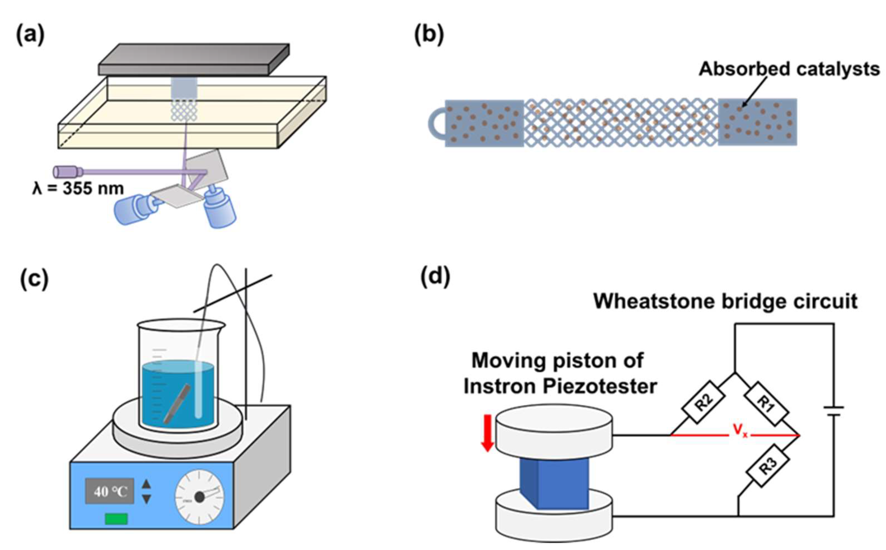
Abstract
:1. Introduction
2. Materials and Methods
2.1. Materials
2.2. VPP 3D Printing
2.3. Electroless Plating
2.3.1. Pretreatment of ELP
2.3.2. Electroless Nickel Plating Process
2.3.3. Electroless Copper Plating Process
2.4. Characterization
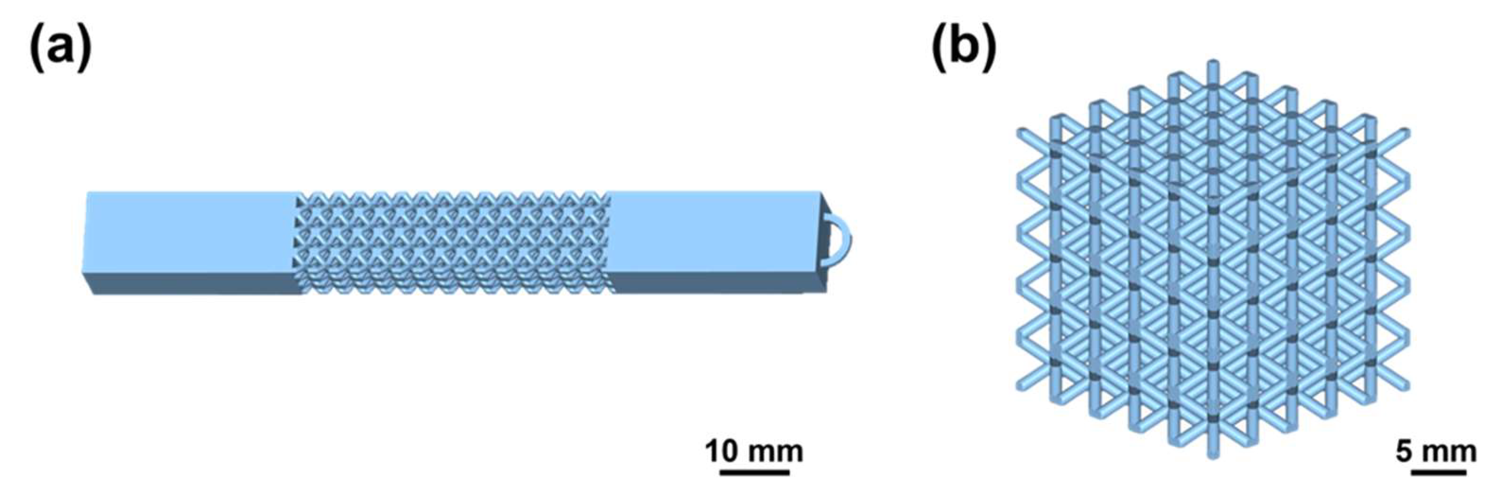
2.5. Demonstrator Design
3. Result and Discussion
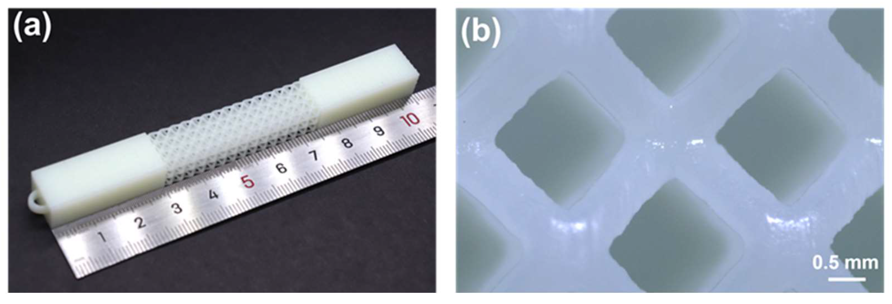
3.1. Quality of VPP 3D Printed Lattice Structures
3.2. Experiments of Electroless Plating Process
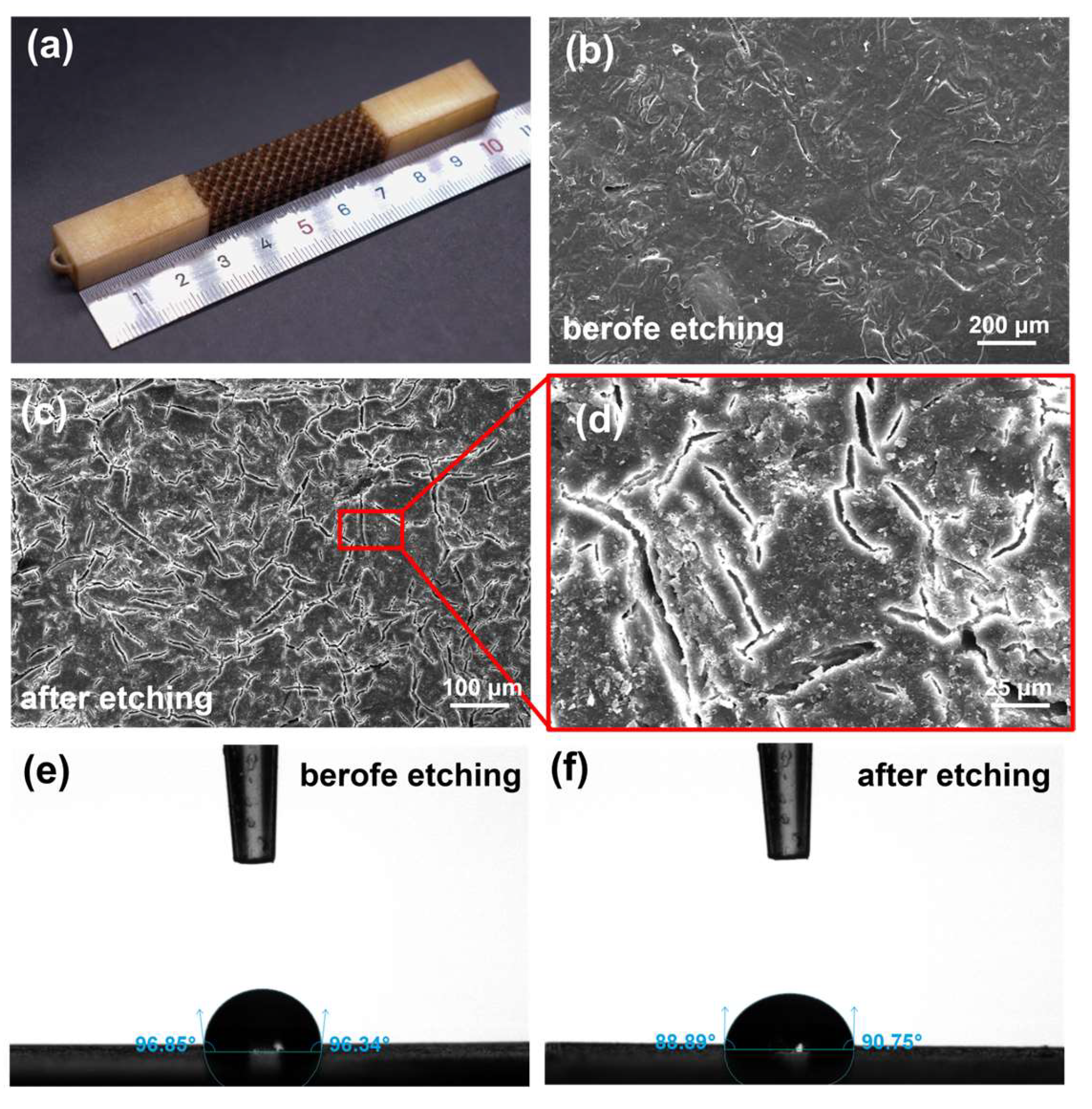
3.2.1. Etching
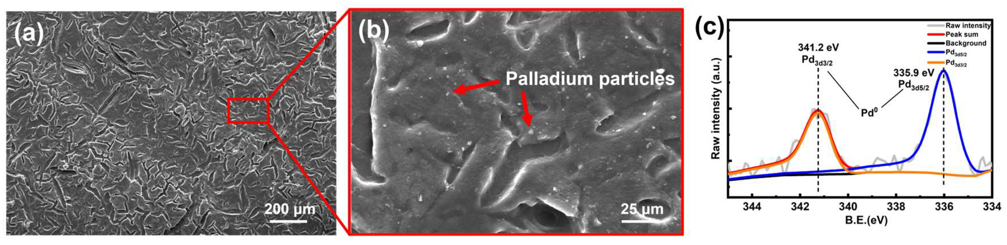
3.2.2. Sensitization-Activation and Acceleration
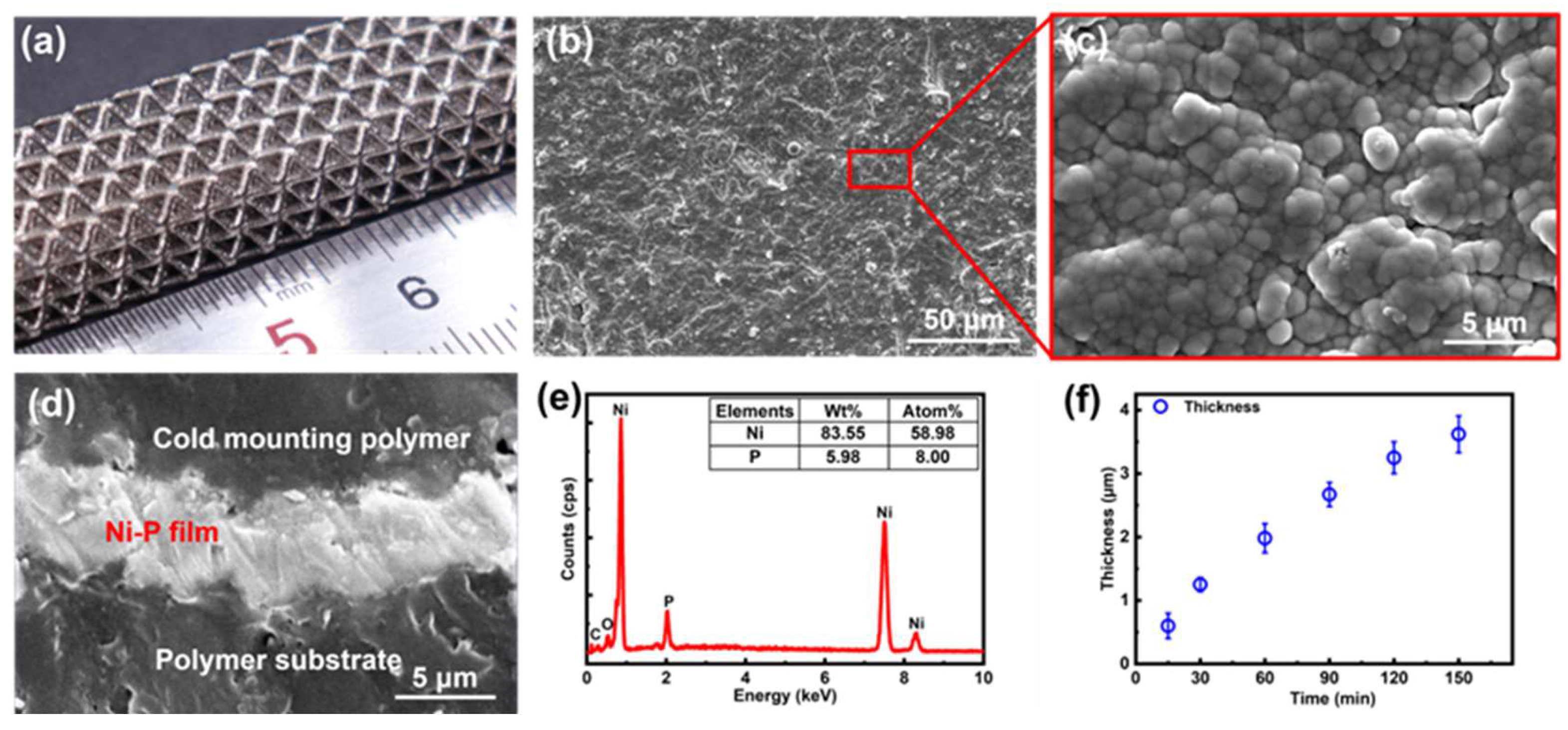
3.2.3. Electroless Nickel Plating Process
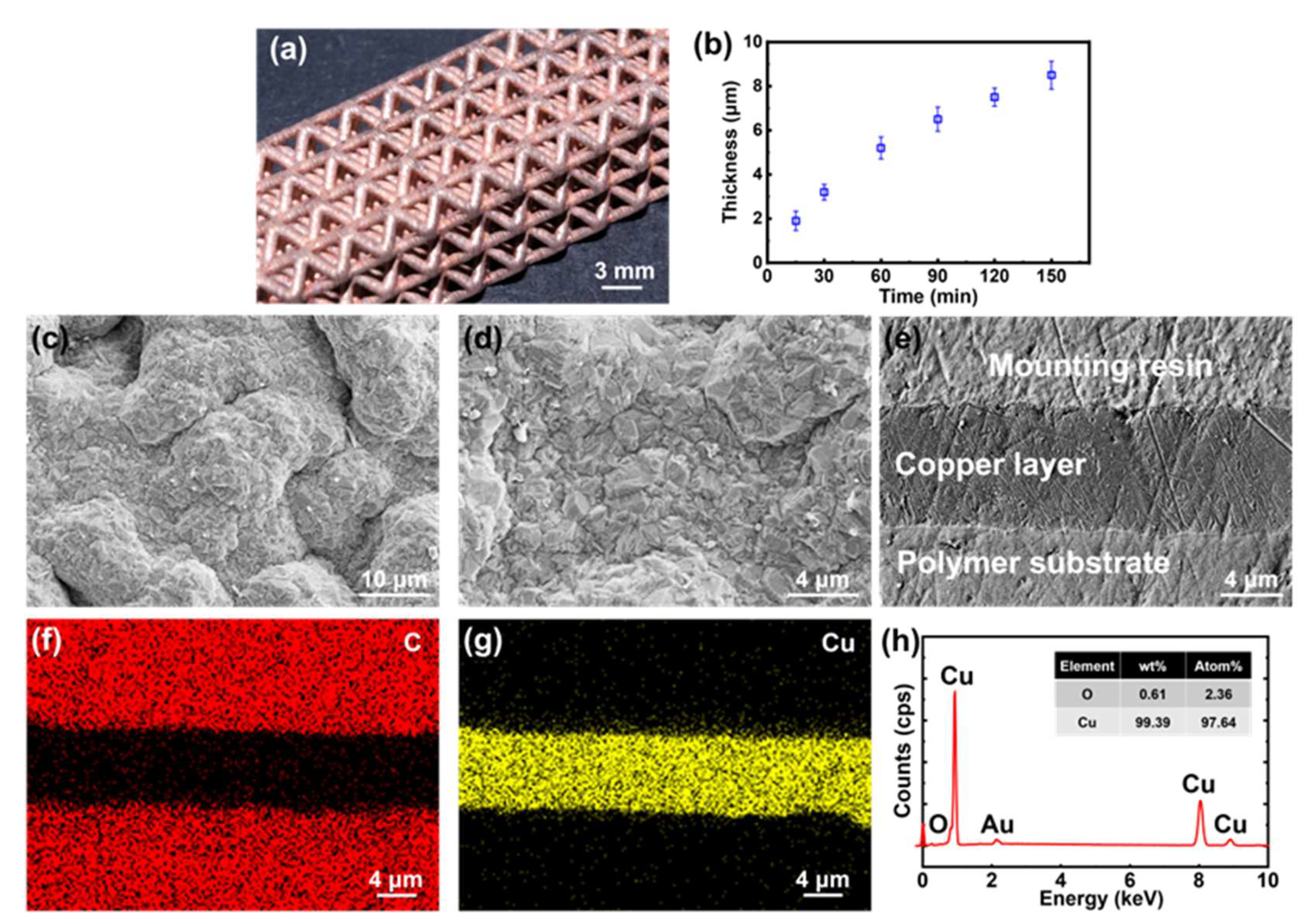
3.2.4. Electroless Copper Plating Process
3.3. Characterization
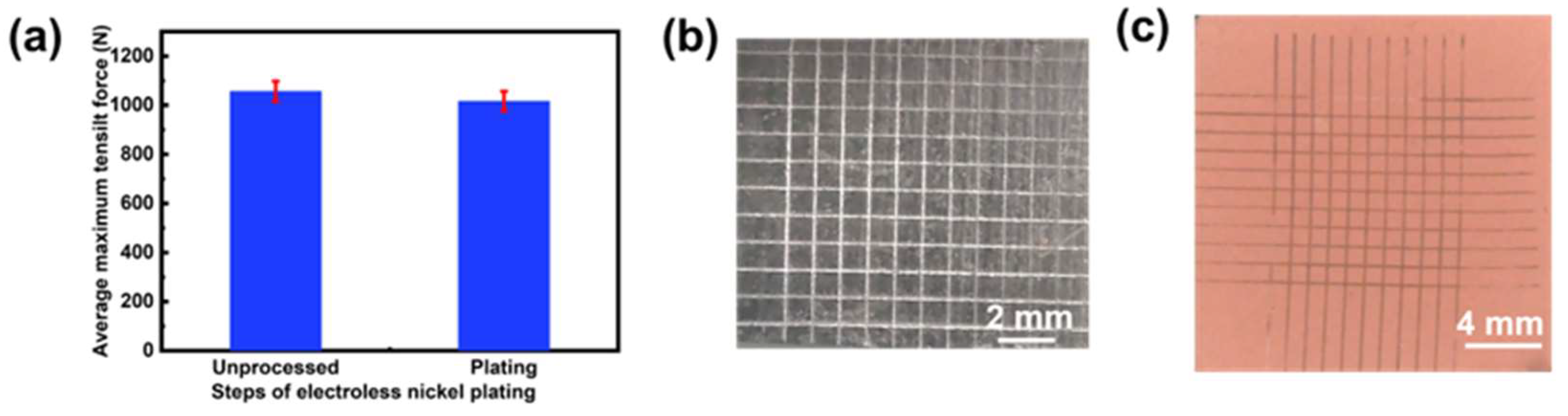
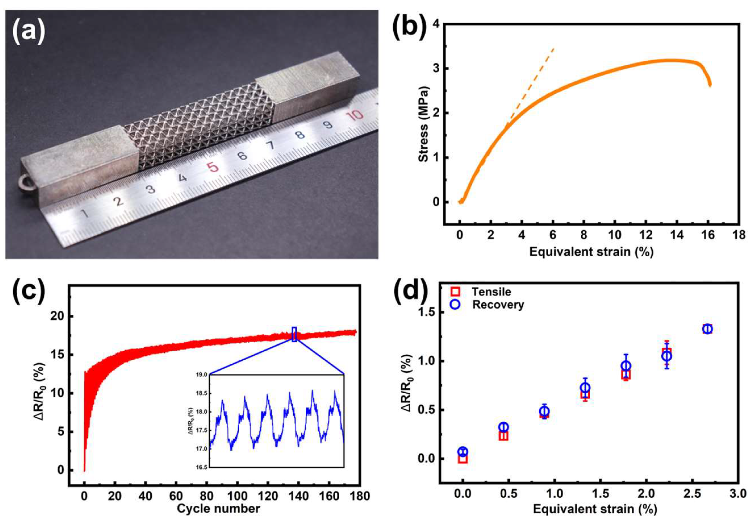
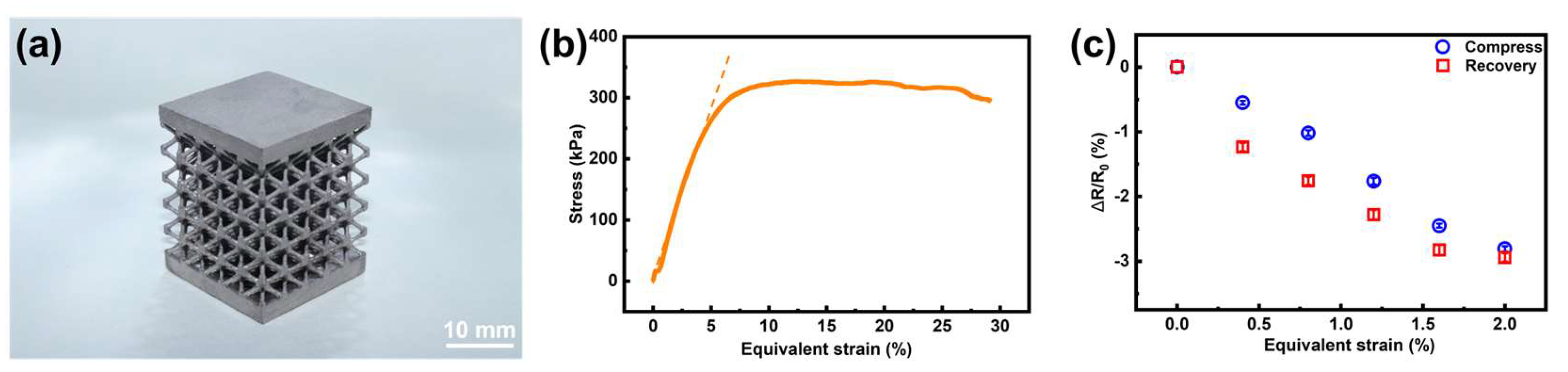
3.3.1. Mechanical Strength
3.3.2. Adhesion Strength
3.4. Demonstrator
4. Conclusions
Author Contributions
Funding
Data Availability Statement
Conflicts of Interest
References
- Maconachie, T.; Leary, M.; Lozanovski, B.; Zhang, X.; Qian, M.; Faruque, O.; Brandt, M. SLM Lattice Structures: Properties, Performance, Applications and Challenges. Mater. Des. 2019, 183, 108137. [Google Scholar] [CrossRef]
- Du, Y.; Li, H.; Luo, Z.; Tian, Q. Topological Design Optimization of Lattice Structures to Maximize Shear Stiffness. Adv. Eng. Softw. 2017, 112, 211–221. [Google Scholar] [CrossRef]
- Zhang, Y.; Chen, F.; Tang, X.; Huang, H.; Chen, T.; Sun, X. Boracic Polyethylene/Polyethylene Wax Blends and Open-Cell Nickel Foams as Neutron-Shielding Composite. J. Reinf. Plast. Compos. 2018, 37, 181–190. [Google Scholar] [CrossRef]
- Zhang, C.; Liu, J.; Yuan, Z.; Xu, S.; Zou, B.; Li, L.; Ma, Y. A Novel Lattice Structure Topology Optimization Method with Extreme Anisotropic Lattice Properties. J. Comput. Des. Eng. 2021, 8, 1367–1390. [Google Scholar] [CrossRef]
- Han, D.; Ren, X.; Luo, C.; Zhang, Y.; Zhang, X.Y.; Zhang, X.G.; Jiang, W.; Hao, J.; Xie, Y.M. Experimental and Computational Investigations of Novel 3D Printed Square Tubular Lattice Metamaterials with Negative Poisson’s Ratio. Addit. Manuf. 2022, 55, 102789. [Google Scholar] [CrossRef]
- Bhullar, S.K.; Ko, J.; Cho, Y.; Jun, M.B.G. Fabrication and Characterization of Nonwoven Auxetic Polymer Stent. Polym. Plast. Technol. Eng. 2015, 54, 1553–1559. [Google Scholar] [CrossRef]
- Song, J.; Gao, L.; Cao, K.; Zhang, H.; Xu, S.; Jiang, C.; Surjadi, J.U.; Xu, Y.; Lu, Y. Metal-Coated Hybrid Meso-Lattice Composites and Their Mechanical Characterizations. Compos. Struct. 2018, 203, 750–763. [Google Scholar] [CrossRef]
- Jin, N.; Wang, F.; Wang, Y.; Zhang, B.; Cheng, H.; Zhang, H. Failure and Energy Absorption Characteristics of Four Lattice Structures under Dynamic Loading. Mater. Des. 2019, 169, 107655. [Google Scholar] [CrossRef]
- Habib, F.N.; Iovenitti, P.; Masood, S.H.; Nikzad, M. Fabrication of Polymeric Lattice Structures for Optimum Energy Absorption Using Multi Jet Fusion Technology. Mater. Des. 2018, 155, 86–98. [Google Scholar] [CrossRef]
- Cramer, N.B.; Cellucci, D.W.; Formoso, O.B.; Gregg, C.E.; Jenett, B.E.; Kim, J.H.; Lendraitis, M.; Swei, S.S.; Trinh, G.T.; Trinh, K.V.; et al. Elastic Shape Morphing of Ultralight Structures by Programmable Assembly. Smart Mater. Struct. 2019, 28, 055006. [Google Scholar] [CrossRef]
- Jenett, B.; Calisch, S.; Cellucci, D.; Cramer, N.; Gershenfeld, N.; Swei, S.; Cheung, K.C. Digital Morphing Wing: Active Wing Shaping Concept Using Composite Lattice-Based Cellular Structures. Soft Robot. 2017, 4, 33–48. [Google Scholar] [CrossRef] [PubMed]
- Sengupta, D.; Prakash Kottapalli, A.G. Ultralight Weight Piezoresistive Spongy Graphene Sensors for Human Gait Monitoring Applications. In Proceedings of the 2020 IEEE 15th International Conference on Nano/Micro Engineered and Molecular System (NEMS), San Diego, CA, USA, 27–30 September 2020; pp. 120–123. [Google Scholar]
- Dong, L.; Deshpande, V.; Wadley, H. Mechanical Response of Ti–6Al–4V Octet-Truss Lattice Structures. Int. J. Solids Struct. 2015, 60–61, 107–124. [Google Scholar] [CrossRef]
- Wadley, H. Fabrication and Structural Performance of Periodic Cellular Metal Sandwich Structures. Compos. Sci. Technol. 2003, 63, 2331–2343. [Google Scholar] [CrossRef]
- Sharp, K.; Mungalov, D.; Brown, J. Metallic Cellular Materials Produced by 3D Weaving. Procedia Mater. Sci. 2014, 4, 15–20. [Google Scholar] [CrossRef]
- Bai, L.; Zhang, J.; Xiong, Y.; Chen, X.; Sun, Y.; Gong, C.; Pu, H.; Wu, X.; Luo, J. Influence of Unit Cell Pose on the Mechanical Properties of Ti6Al4V Lattice Structures Manufactured by Selective Laser Melting. Addit. Manuf. 2020, 34, 101222. [Google Scholar] [CrossRef]
- Wang, Z.; Luan, C.; Liao, G.; Yao, X.; Fu, J. Mechanical and Self-Monitoring Behaviors of 3D Printing Smart Continuous Carbon Fiber-Thermoplastic Lattice Truss Sandwich Structure. Compos. Part B Eng. 2019, 176, 107215. [Google Scholar] [CrossRef]
- Xiao, R.; Feng, X.; Fan, R.; Chen, S.; Song, J.; Gao, L.; Lu, Y. 3D Printing of Titanium-Coated Gradient Composite Lattices for Lightweight Mandibular Prosthesis. Compos. Part B Eng. 2020, 193, 108057. [Google Scholar] [CrossRef]
- Hou, W.; He, P.; Yang, Y.; Sang, L. Crashworthiness Optimization of Crash Box with 3D-Printed Lattice Structures. Int. J. Mech. Sci. 2023, 247, 108198. [Google Scholar] [CrossRef]
- Clough, E.C.; Plaisted, T.A.; Eckel, Z.C.; Cante, K.; Hundley, J.M.; Schaedler, T.A. Elastomeric Microlattice Impact Attenuators. Matter 2019, 1, 1519–1531. [Google Scholar] [CrossRef]
- Abyzova, E.; Petrov, I.; Bril’, I.; Cheshev, D.; Ivanov, A.; Khomenko, M.; Averkiev, A.; Fatkullin, M.; Kogolev, D.; Bolbasov, E.; et al. Universal Approach to Integrating Reduced Graphene Oxide into Polymer Electronics. Polymers 2023, 15, 4622. [Google Scholar] [CrossRef]
- MacDonald, E.; Wicker, R. Multiprocess 3D Printing for Increasing Component Functionality. Science 2016, 353, aaf2093. [Google Scholar] [CrossRef] [PubMed]
- Deng, F.; Nguyen, Q.-K.; Zhang, P. Multifunctional Liquid Metal Lattice Materials through Hybrid Design and Manufacturing. Addit. Manuf. 2020, 33, 101117. [Google Scholar] [CrossRef]
- Ming Yin, Y.; Yang Li, H.; Xu, J.; Zhang, C.; Liang, F.; Li, X.; Jiang, Y.; Wei Cao, J.; Fang Feng, H.; Nan Mao, J.; et al. Facile Fabrication of Flexible Pressure Sensor with Programmable Lattice Structure. ACS Appl. Mater. Interfaces 2021, 13, 10388–10396. [Google Scholar] [CrossRef]
- Kamat, A.M.; Kottapalli, A.G.P. 3D Printed Graphene-Coated Flexible Lattice as Piezoresistive Pressure Sensor. In Proceedings of the 2021 IEEE 21st International Conference on Solid-State Sensors, Actuators and Microsystems (Transducers), Orlando, FL, USA, 20–24 June 2021; pp. 888–891. [Google Scholar]
- Delaunois, F.; Vitry, V.; Bonin, L. (Eds.) Electroless Nickel Plating; CRC Press: Boca Raton, FL, USA, 2019; ISBN 9780429466274. [Google Scholar]
- Ashkenazi, D.; Inberg, A.; Shacham-Diamand, Y.; Stern, A. Gold, Silver, and Electrum Electroless Plating on Additively Manufactured Laser Powder-Bed Fusion AlSi10Mg Parts: A Review. Coatings 2021, 11, 422. [Google Scholar] [CrossRef]
- Ghosh, S. Electroless Copper Deposition: A Critical Review. Thin Solid Films 2019, 669, 641–658. [Google Scholar] [CrossRef]
- Hensleigh, R.; Cui, H.; Xu, Z.; Massman, J.; Yao, D.; Berrigan, J.; Zheng, X. Charge-Programmed Three-Dimensional Printing for Multi-Material Electronic Devices. Nat. Electron. 2020, 3, 216–224. [Google Scholar] [CrossRef]
- Shin, C.S.; Chang, Y.C. Fabrication and Compressive Behavior of a Micro-Lattice Composite by High Resolution DLP Stereolithography. Polymers 2021, 13, 785. [Google Scholar] [CrossRef] [PubMed]
- Li, J.; Zhang, Y.; Wang, P.; Wang, G.; Liu, Y.; Liu, Y.; Li, Q. Selectively Metalizable Stereolithography Resin for Three-Dimensional DC and High-Frequency Electronics via Hybrid Additive Manufacturing. ACS Appl. Mater. Interfaces 2021, 13, 22891–22901. [Google Scholar] [CrossRef]
- Wang, P.; Li, J.; Wang, G.; Hai, Y.; He, L.; Yu, Y.; Wang, X.; Chen, M.; Xu, B. Selectively Metalizable Low-Temperature Cofired Ceramic for Three-Dimensional Electronics via Hybrid Additive Manufacturing. ACS Appl. Mater. Interfaces 2022, 14, 28060–28073. [Google Scholar] [CrossRef]
- Wang, P.; Li, J.; Yang, J.; Wang, G.; He, L.; Zhang, H. Enabling 3D Multilayer Electronics through the Hybrid of Vat Photopolymerization and Laser-Activated Selective Metallization. Addit. Manuf. 2023, 74, 103717. [Google Scholar] [CrossRef]
- Wang, P.; Li, J.; Wang, G.; He, L.; Yang, J.; Zhang, C.; Han, Z.; Yan, Y. Hybrid Additive Manufacturing Based on Vat Photopolymerization and Laser-Activated Selective Metallization for Three-Dimensional Conformal Electronics. Addit. Manuf. 2023, 63, 103388. [Google Scholar] [CrossRef]
- Wang, P.; Li, J.; Deng, L.; Liu, S.; Wang, G.; Huang, J.; Tang, X.; Han, L. Laser-Activated Selective Electroless Plating on 3D Structures via Additive Manufacturing for Customized Electronics. Adv. Mater. Technol. 2023, 8, 2300516. [Google Scholar] [CrossRef]
- Shacham-Diamand, Y.; Osaka, T.; Okinaka, Y.; Sugiyama, A.; Dubin, V. 30 Years of Electroless Plating for Semiconductor and Polymer Micro-Systems. Microelectron. Eng. 2015, 132, 35–45. [Google Scholar] [CrossRef]
- Xuan, N.; Chen, J.; Shi, J.; Yue, Y.; Zhuang, P.; Ba, K.; Sun, Y.; Shen, J.; Liu, Y.; Ge, B.; et al. Single-Atom Electroplating on Two Dimensional Materials. Chem. Mater. 2019, 31, 429–435. [Google Scholar] [CrossRef]
- ASTM D3359-09; Standard Test Methods for Measuring Adhesion by Tape Test. ASTM: West Conshohocken, PA, USA, 2009.
- Zheng, Y.; Li, Y.; Dai, K.; Liu, M.; Zhou, K.; Zheng, G.; Liu, C.; Shen, C. Conductive Thermoplastic Polyurethane Composites with Tunable Piezoresistivity by Modulating the Filler Dimensionality for Flexible Strain Sensors. Compos. Part A Appl. Sci. Manuf. 2017, 101, 41–49. [Google Scholar] [CrossRef]
- Zheng, Y.; Li, Y.; Zhou, Y.; Dai, K.; Zheng, G.; Zhang, B.; Liu, C.; Shen, C. High-Performance Wearable Strain Sensor Based on Graphene/Cotton Fabric with High Durability and Low Detection Limit. ACS Appl. Mater. Interfaces 2020, 12, 1474–1485. [Google Scholar] [CrossRef]


Disclaimer/Publisher’s Note: The statements, opinions and data contained in all publications are solely those of the individual author(s) and contributor(s) and not of MDPI and/or the editor(s). MDPI and/or the editor(s) disclaim responsibility for any injury to people or property resulting from any ideas, methods, instructions or products referred to in the content. |
© 2023 by the authors. Licensee MDPI, Basel, Switzerland. This article is an open access article distributed under the terms and conditions of the Creative Commons Attribution (CC BY) license (https://creativecommons.org/licenses/by/4.0/).
Share and Cite
He, L.; Wang, P.; Yang, J.; Fan, K.; Zhang, H.; Zhang, L.; Jiang, M.; Chen, X.; Chen, Z.; Chen, M.; et al. Smart Lattice Structures with Self-Sensing Functionalities via Hybrid Additive Manufacturing Technology. Micromachines 2024, 15, 2. https://doi.org/10.3390/mi15010002
He L, Wang P, Yang J, Fan K, Zhang H, Zhang L, Jiang M, Chen X, Chen Z, Chen M, et al. Smart Lattice Structures with Self-Sensing Functionalities via Hybrid Additive Manufacturing Technology. Micromachines. 2024; 15(1):2. https://doi.org/10.3390/mi15010002
Chicago/Turabian StyleHe, Liu, Peiren Wang, Junhui Yang, Kaoyi Fan, Hanqiang Zhang, Luyan Zhang, Mingxing Jiang, Xiaoyi Chen, Zhen Chen, Min Chen, and et al. 2024. "Smart Lattice Structures with Self-Sensing Functionalities via Hybrid Additive Manufacturing Technology" Micromachines 15, no. 1: 2. https://doi.org/10.3390/mi15010002