
Design of a Penta-Band Graphene-Based Terahertz Metamaterial Absorber with Fine Sensing Performance
 , , , and
Abstract
:1. Introduction
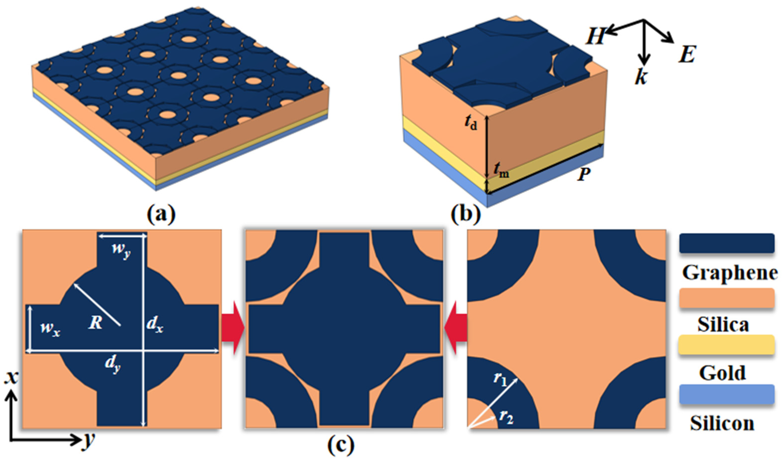
2. Structure and Design
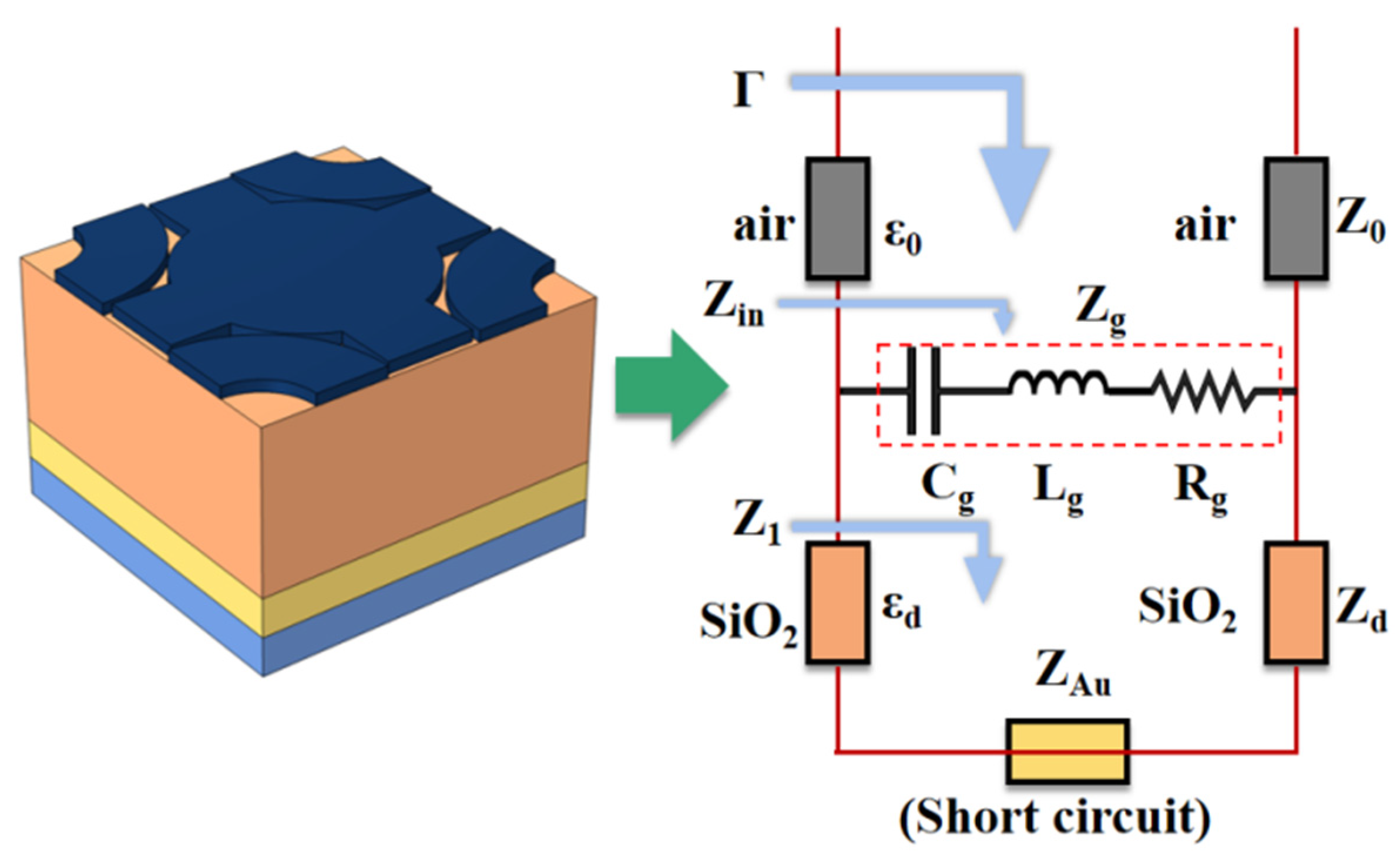
3. Simulation Process
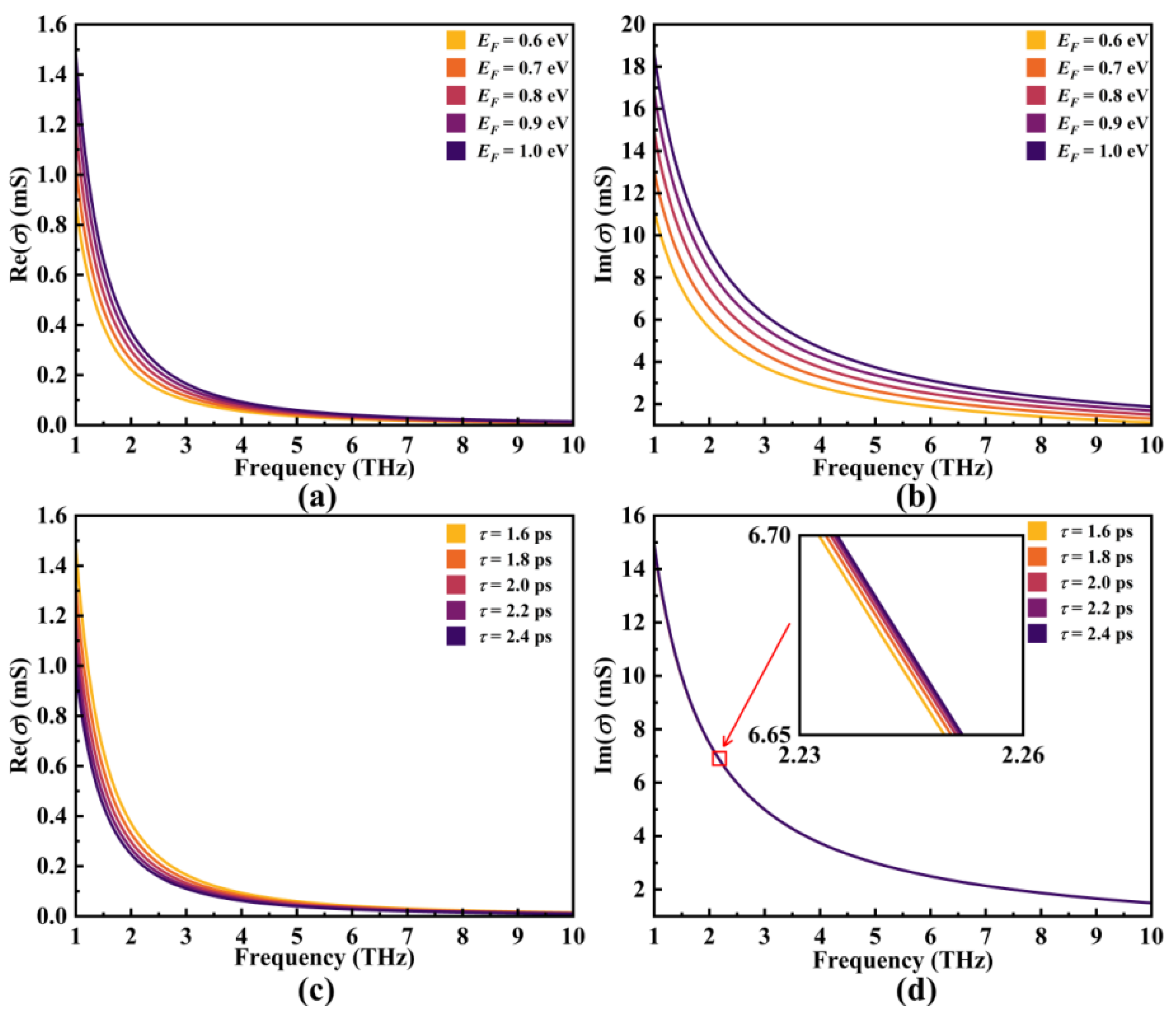
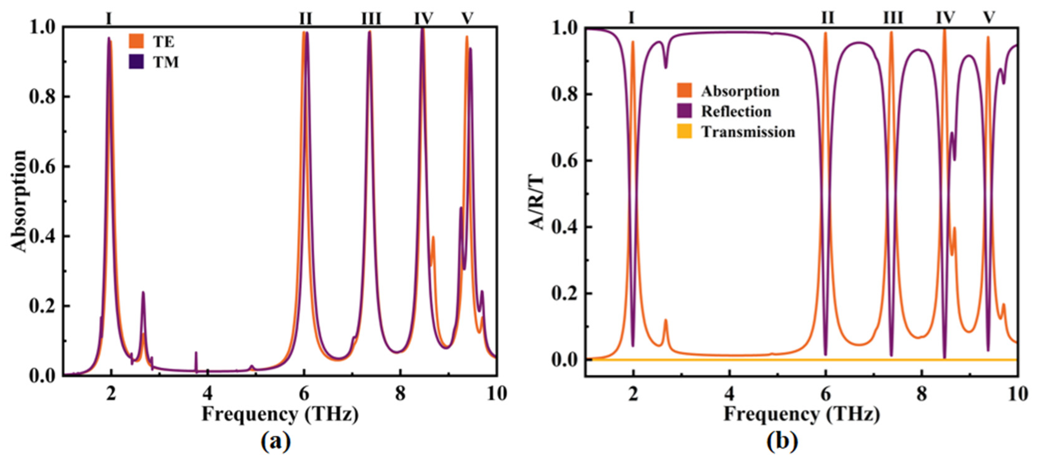
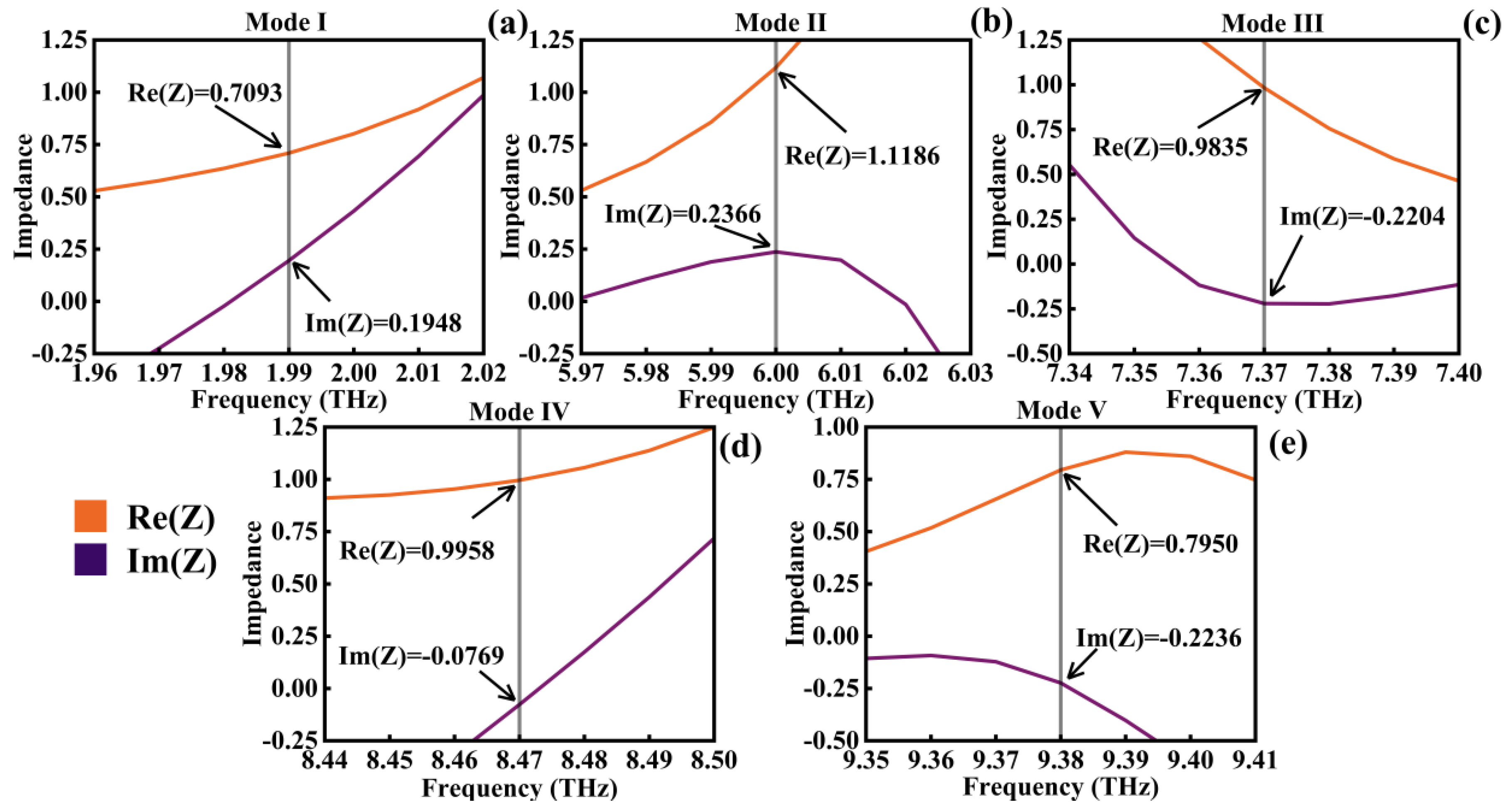
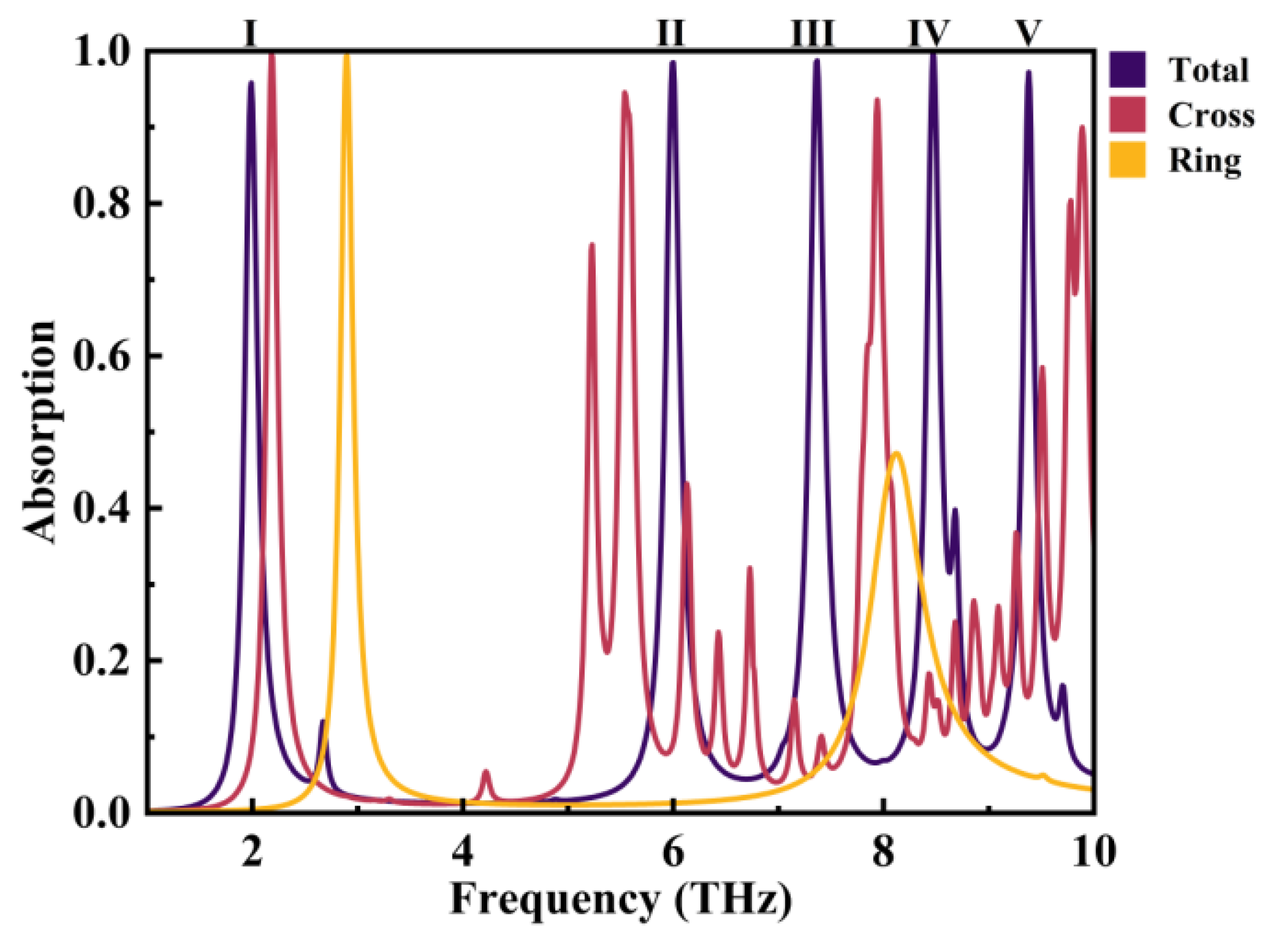
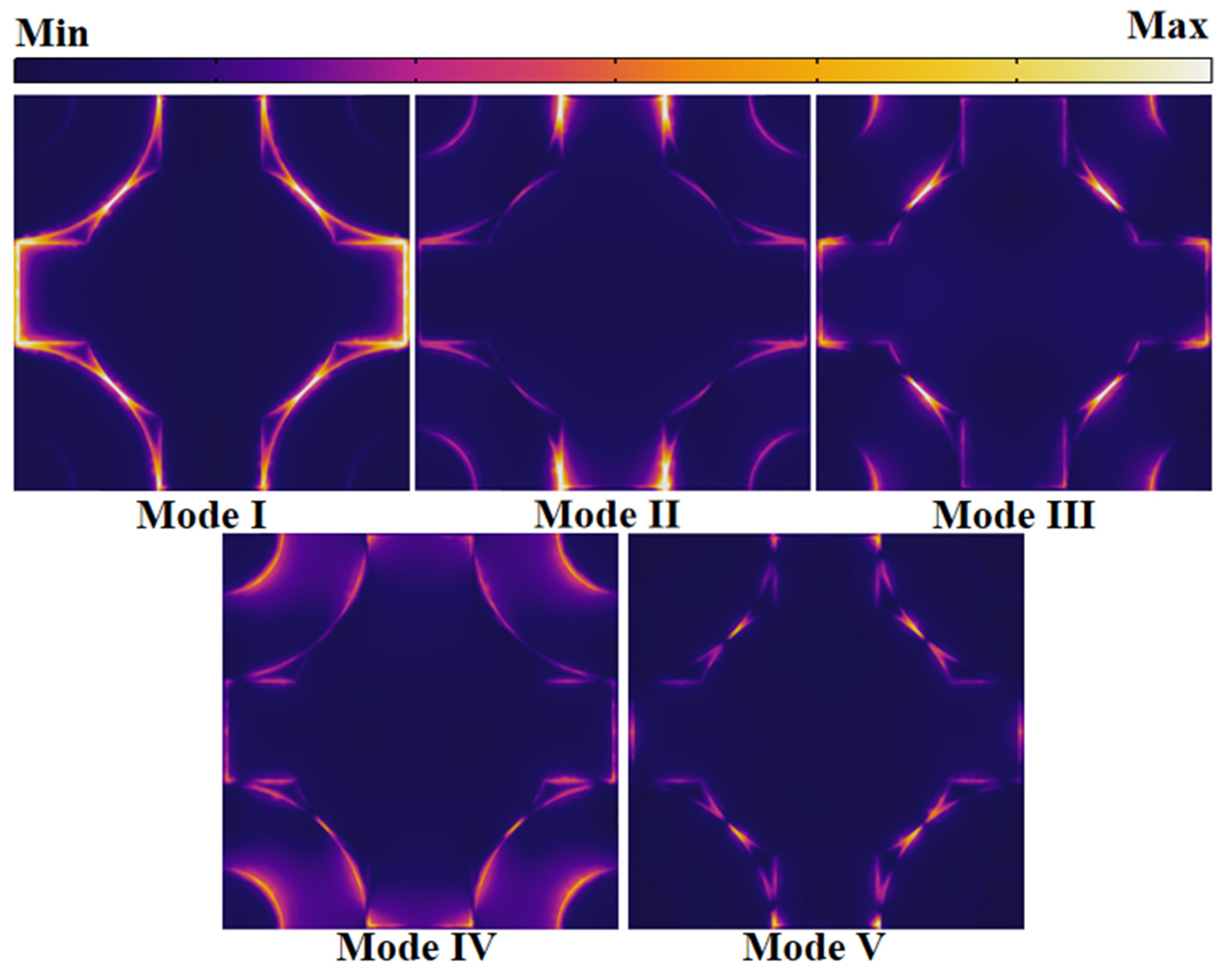
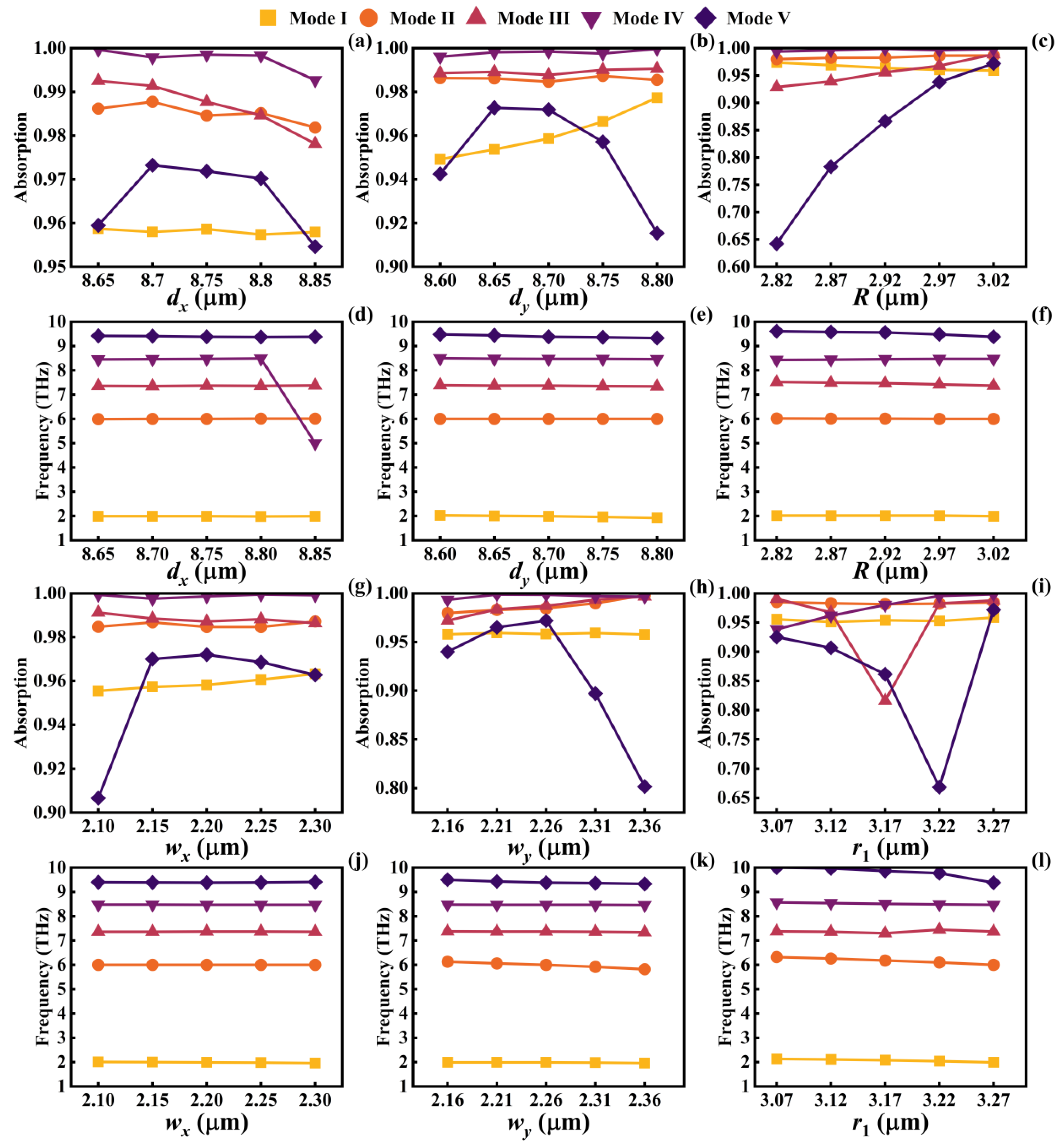
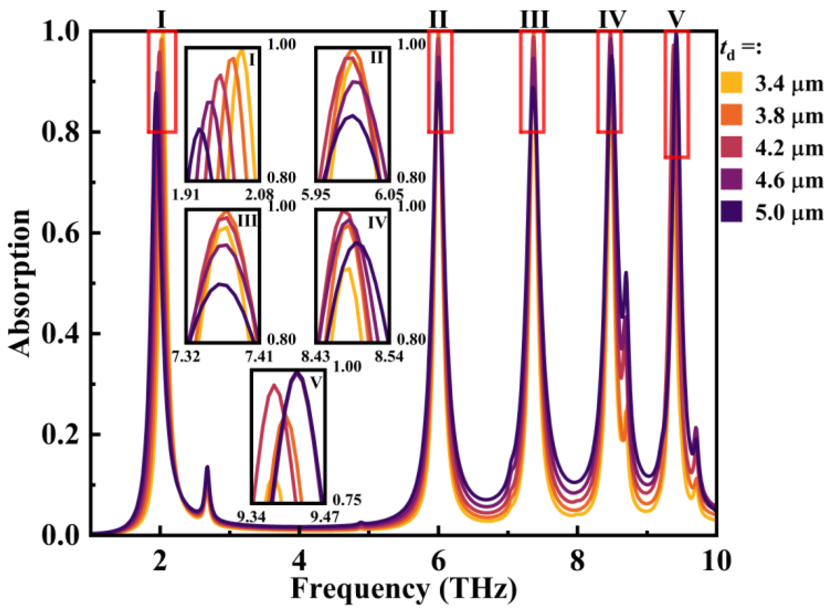
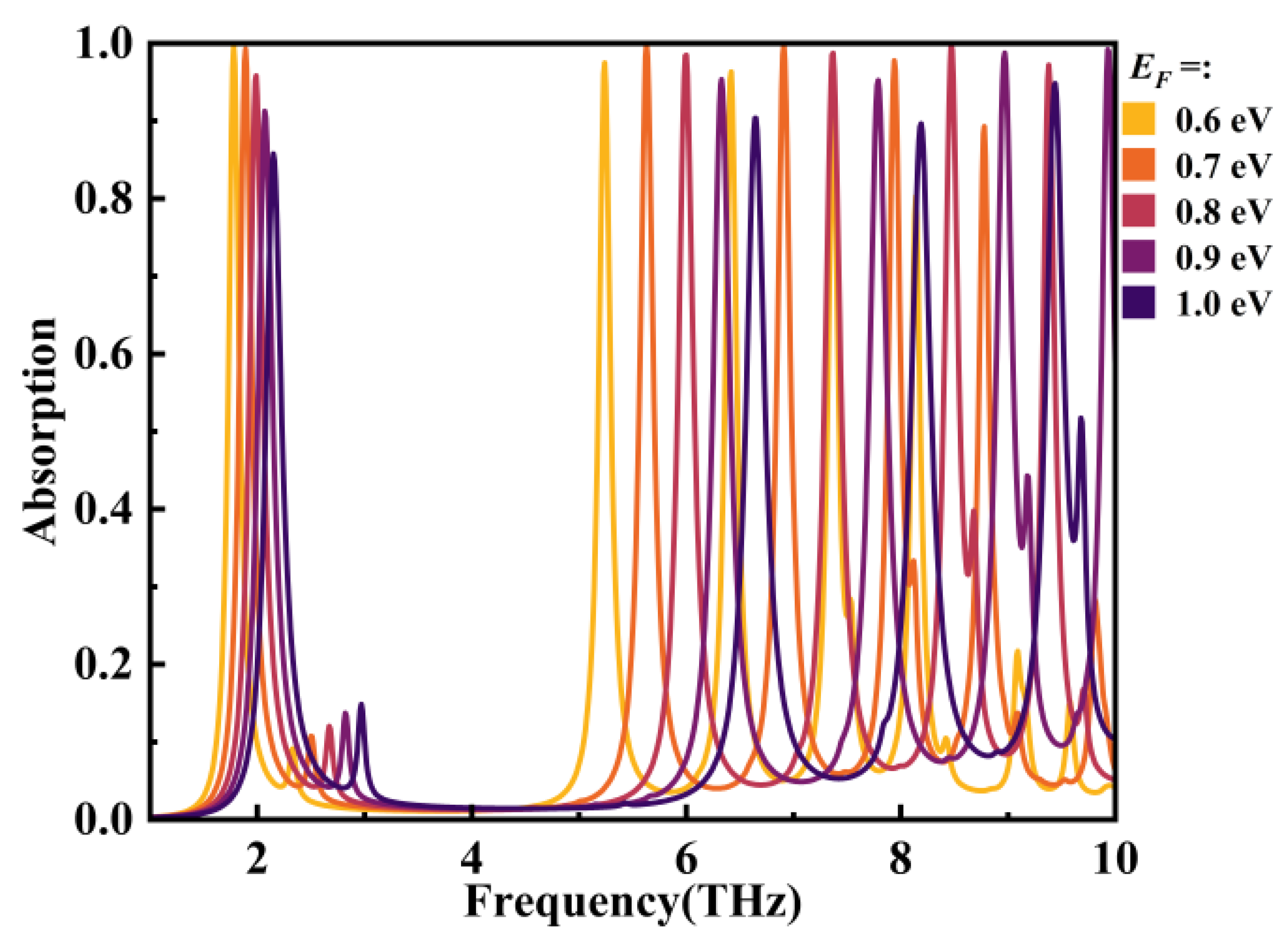
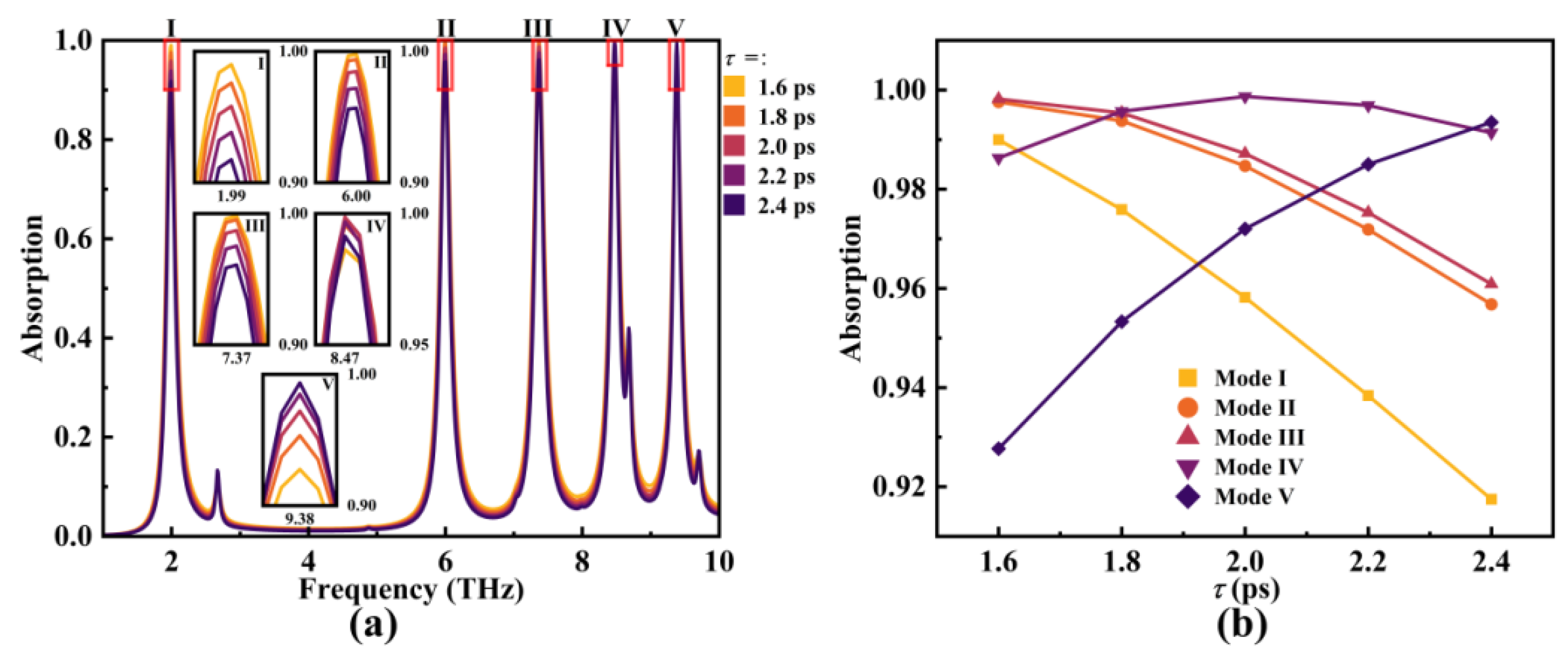
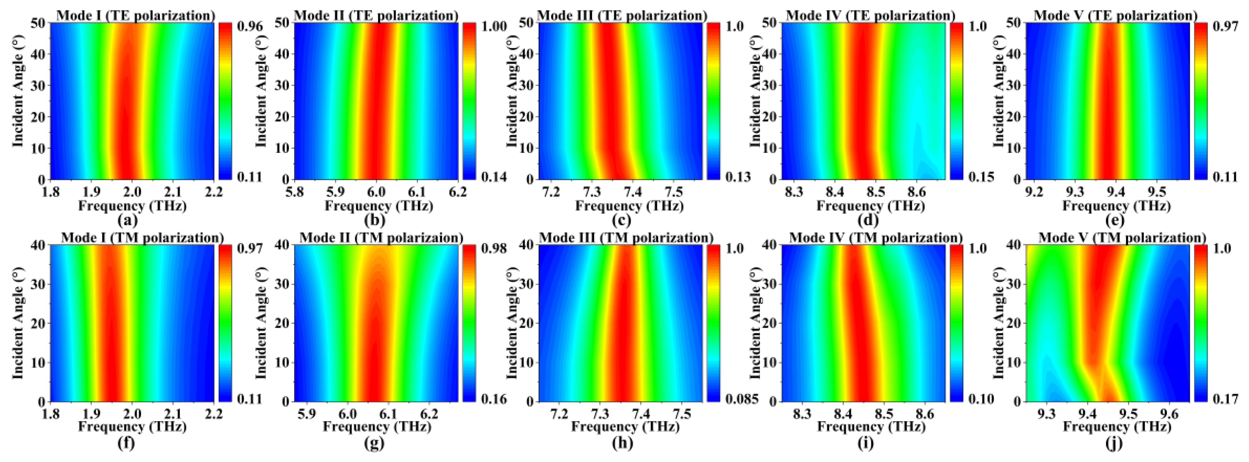
4. Simulation Results and Discussion
5. Conclusions
Author Contributions
Funding
Institutional Review Board Statement
Informed Consent Statement
Data Availability Statement
Conflicts of Interest
References
- Krasikov, S.; Tranter, A.; Bogdanov, A.; Kivshar, Y. Intelligent metaphotonics empowered by machine learning. Opto Electron. Adv. 2022, 5, 210147. [Google Scholar] [CrossRef]
- Wu, F.Y.; Shi, P.C.; Yi, Z.; Li, H.L.; Yi, Y.G. Ultra-Broadband Solar Absorber and High-Efficiency Thermal Emitter from UV to Mid-Infrared Spectrum. Micromachines 2023, 14, 985. [Google Scholar] [CrossRef]
- Biabanifard, M.; Abrishamian, M.S. Circuit Modeling of Tunable Terahertz Graphene Absorber. Optik 2018, 158, 842–849. [Google Scholar] [CrossRef]
- Yang, J.; Lin, Y.-S. Design of Tunable Terahertz Metamaterial Sensor with Single- and Dual-Resonance Characteristic. Nanomaterials 2021, 11, 2212. [Google Scholar] [CrossRef]
- Song, Z.; Wang, K.; Li, J.; Liu, Q.H. Broadband Tunable Terahertz Absorber Based on Vanadium Dioxide Metamaterials. Opt. Express 2018, 26, 7148–7154. [Google Scholar] [CrossRef]
- Shen, Y.; Liang, L.; Zhang, S.; Huang, D.; Zhang, J.; Xu, S.; Liang, C.; Xu, W. Thermally and Electrically Dual-Tunable Absorber Based on Dirac Semimetal and Strontium Titanate. Nanoscale 2018, 10, 1622–1630. [Google Scholar] [CrossRef]
- Wu, X.; Yin, C.; Zhang, M.; Xie, Y.; Hu, J.; Long, R.; Wu, X.; Wu, X. The Intercalation Cathode of MOFs-driven Vanadium-based Composite Embedded in N-doped Carbon for Aqueous Zinc ion Batteries. Chem. Eng. J. 2023, 452, 139573. [Google Scholar] [CrossRef]
- Li, J.; Liu, G.; Liu, B.; Min, Z.; Qian, D.; Jiang, J.; Li, J. An extremely facile route to Co2P encased in N,P-codoped carbon layers: Highly efficient bifunctional electrocatalysts for ORR and OER. Int. J. Hydrogen Energy 2018, 43, 1365–1374. [Google Scholar] [CrossRef]
- Chen, Z.H.; Cai, P.G.; Wen, Q.Y.; Chen, H.; Tang, Y.J.; Yi, Z.; Wei, K.H.; Li, G.F.; Tang, B.; Yi, Y.G. Graphene Multi-Frequency Broadband and Ultra-Broadband Terahertz Absorber Based on Surface Plasmon Resonance. Electronics 2023, 12, 2655. [Google Scholar] [CrossRef]
- Li, K.; Yu, J. Photonics-Aided Terahertz-Wave Wireless Communication. J. Light. Technol. 2022, 40, 4186–4195. [Google Scholar] [CrossRef]
- Liang, S.R.; Xu, F.; Li, W.X.; Yang, W.X.; Cheng, S.B.; Yang, H.; Chen, J.; Yi, Z.; Jiang, P.P. Tunable smart mid infrared thermal control emitter based on phase change material VO2 thin film. Appl. Therm. Eng. 2023, 232, 121074. [Google Scholar] [CrossRef]
- Kats, M.A.; Capasso, F. Optical Absorbers Based on Strong Interference in Ultra-thin Films. Laser Photonics Rev. 2016, 10, 735–749. [Google Scholar] [CrossRef]
- Kazanskiy, N.L.; Khonina, S.N.; Butt, M.A. Recent Development in Metasurfaces: A Focus on Sensing Applications. Nanomaterials 2023, 13, 118. [Google Scholar] [CrossRef]
- Abou Houran, M.; Alsharai, M.; Baqir, M.A.; Saqlain, M.; Dhasarathan, V. Polarization-Insensitive and Wide-Angle Absorber Operating in the Visible and near-Infrared Regimes. Optik 2023, 283, 170915. [Google Scholar] [CrossRef]
- Zou, Y.; Chen, S.; Sun, J.; Zhou, S. Mid-Infrared Pyroelectric Detector with Metasurface Electrode for Broadband Enhanced Absorption. J. Phys. D Appl. Phys. 2023, 56, 445105. [Google Scholar] [CrossRef]
- Bouanane, I.; Bedu, F.; Ozerov, I.; Sciacca, B.; Santinacci, L.; Duché, D.; Berginc, G.; Escoubas, L.; Margeat, O.; Le Rouzo, J. Design of Infrared Optical Absorber Using Silver Nanorings Array Made by a Top-down Process. Sci. Rep. 2023, 13, 7770. [Google Scholar] [CrossRef] [PubMed]
- Li, S.-J.; Wu, P.-X.; Xu, H.-X.; Zhou, Y.-L.; Cao, X.-Y.; Han, J.-F.; Zhang, C.; Yang, H.-H.; Zhang, Z. Ultra-Wideband and Polarization-Insensitive Perfect Absorber Using Multilayer Metamaterials, Lumped Resistors, and Strong Coupling Effects. Nanoscale Res. Lett. 2018, 13, 386. [Google Scholar] [CrossRef] [PubMed]
- Vafapour, Z.; Ghahraloud, H.; Keshavarz, A.; Islam, M.S.; Rashidi, A.; Dutta, M.; Stroscio, M.A. The Potential of Refractive Index Nanobiosensing Using a Multi-Band Optically Tuned Perfect Light Metamaterial Absorber. IEEE Sens. J. 2021, 21, 13786–13793. [Google Scholar] [CrossRef]
- Liang, Y.; Lin, H.; Lin, S.; Wu, J.; Li, W.; Meng, F.; Yang, Y.; Huang, X.; Jia, B.; Kivshar, Y. Hybrid Anisotropic Plasmonic Metasurfaces with Multiple Resonances of Focused Light Beams. Nano Lett. 2021, 21, 8917–8923. [Google Scholar] [CrossRef]
- Stewart, J.W.; Nebabu, T.; Mikkelsen, M.H. Control of Nanoscale Heat Generation with Lithography-Free Metasurface Absorbers. Nano Lett. 2022, 22, 5151–5157. [Google Scholar] [CrossRef]
- Qi, Y.; Yang, L.; Yue, L.; Li, J.; Wang, X.; Sun, Z.; Cao, J. Theoretical Studies of the THz Compression of Low-to-Medium Energy Electron Pulses and the Single-Shot Stamping of Electron–THz Timing Jitter. N. J. Phys. 2021, 23, 063052. [Google Scholar] [CrossRef]
- Sun, S.; Liu, S.; Zhong, S. Analysis of Terahertz Wave Penetration Capacity to 2D Conductive Cylinder Coated with Steady-State Parabolic Distribution Plasma Media. Results Phys. 2021, 27, 104516. [Google Scholar] [CrossRef]
- Shi, S.-C.; Paine, S.; Yao, Q.-J.; Lin, Z.-H.; Li, X.-X.; Duan, W.-Y.; Matsuo, H.; Zhang, Q.; Yang, J.; Ashley, M.C.B.; et al. Terahertz and Far-Infrared Windows Opened at Dome A in Antarctica. Nat. Astron. 2016, 1, 0001. [Google Scholar] [CrossRef]
- Bowman, T.C.; El-Shenawee, M.; Campbell, L.K. Terahertz Imaging of Excised Breast Tumor Tissue on Paraffin Sections. IEEE Trans. Antennas Propag. 2015, 63, 2088–2097. [Google Scholar] [CrossRef]
- Mason, M.J.; Coleman, B.J.; Saha, S.; Mustafa, M.M.; Green, M.J. Graphene Signatures: Identifying Graphite and Graphene Grades via Radio Frequency Heating. Carbon 2021, 182, 564–570. [Google Scholar] [CrossRef]
- Wang, L.; Wang, W.; Xu, G.; Ji, Z.; Lu, N.; Li, L.; Liu, M. Analytical Carrier Density and Quantum Capacitance for Graphene. Appl. Phys. Lett. 2016, 108, 013503. [Google Scholar] [CrossRef]
- Liu, J.; Fan, L.; Su, J.; Yang, S.; Luo, H.; Shen, X.; Ding, F. Terahertz Time Domain Spectroscopic Response towards Different Macrocyclic Antibiotics Using a One-Step Transfer Graphene Metamaterial Absorber. Mater. Chem. Phys. 2022, 292, 126784. [Google Scholar] [CrossRef]
- Wang, X.; Wang, Y.; Yang, X.; Cao, Y. Numerical Simulation on the LSPR-Effective Core-Shell Copper/Graphene Nanofluids. Sol. Energy 2019, 181, 439–451. [Google Scholar] [CrossRef]
- Park, M.J.; Choi, H.-H.; Park, B.; Lee, J.Y.; Lee, C.-H.; Choi, Y.S.; Kim, Y.; Yoo, J.M.; Lee, H.; Hong, B.H. Enhanced Chemical Reactivity of Graphene by Fermi Level Modulation. Chem. Mater. 2018, 30, 5602–5609. [Google Scholar] [CrossRef]
- Yan, D.; Li, J. Tunable All-Graphene-Dielectric Single-Band Terahertz Wave Absorber. J. Phys. D Appl. Phys. 2019, 52, 275102. [Google Scholar] [CrossRef]
- Zhu, X.; Wang, B. Graphene-Based Angle-Insensitive and Tunable Single-Band and Dual-Band Metamaterial Terahertz Absorber. Phys. Status Solidi (b) 2022, 259, 2100573. [Google Scholar] [CrossRef]
- Lai, R.; Shi, P.; Yi, Z.; Li, H.; Yi, Y. Triple-Band Surface Plasmon Resonance Metamaterial Absorber Based on Open-Ended Prohibited Sign Type Monolayer Graphene. Micromachines 2023, 14, 953. [Google Scholar] [CrossRef] [PubMed]
- Barnes, W.L.; Dereux, A.; Ebbesen, T.W. Surface Plasmon Subwavelength Optics. Nature 2003, 424, 824–830. [Google Scholar] [CrossRef] [PubMed]
- Gao, S.Y.; Wei, K.H.; Yang, H.; Tang, Y.J.; Yi, Z.; Tang, C.J.; Tang, B.; Yi, Y.G.; Wu, P.H. Design of Surface Plasmon Reso-nance-Based D-Type Double Open-Loop Channels PCF for Temperature Sensing. Sensors 2023, 23, 7569. [Google Scholar] [CrossRef]
- Meng, W.; Li, C.; Yao, M.; He, Z.; Wu, X.; Jiang, Z.; Dai, L.; Wang, L. Synthesis and electrochemical performance of Li1+xTi2−xFex(PO4)3/C anode for aqueous lithium ion battery. Adv. Powder Technol. 2020, 31, 1359–1364. [Google Scholar] [CrossRef]
- Huang, C.; Ji, C.; Zhao, B.; Peng, J.; Yuan, L.; Luo, X. Multifunctional and Tunable Radar Absorber Based on Graphene-Integrated Active Metasurface. Adv. Mater. Technol. 2021, 6, 2001050. [Google Scholar] [CrossRef]
- Mohsen Daraei, O.; Goudarzi, K.; Bemani, M. A Tunable Ultra-Broadband Terahertz Absorber Based on Two Layers of Graphene Ribbons. Opt. Laser Technol. 2020, 122, 105853. [Google Scholar] [CrossRef]
- Zhu, Y.Y.; Cai, P.G.; Zhang, W.L.; Meng, T.Y.; Tang, Y.J.; Yi, Z.; Wei, K.H.; Li, G.F.; Tang, B.; Yi, Y.G. Ultra-Wideband High-Efficiency Solar Absorber and Thermal Emitter Based on Semiconductor InAs Microstructures. Micromachines 2023, 14, 1597. [Google Scholar] [CrossRef]
- Nickpay, M.-R.; Danaie, M.; Shahzadi, A. A Triple-band Metamaterial Graphene-Based Absorber Using Rotated Split-Ring Resonators for THz Biomedical Sensing. Opt. Quantum Electron. 2023, 55, 193. [Google Scholar] [CrossRef]
- Barzegar-Parizi, S.; Khavasi, A. Designing Dual-Band Absorbers by Graphene/Metallic Metasurfaces. IEEE J. Quantum Electron. 2019, 55, 1–8. [Google Scholar] [CrossRef]
- Liu, W.; Liu, C.; Wang, J.X.; Lv, J.W.; Lv, Y.; Yang, L.; An, N.; Yi, Z.; Liu, Q.; Hu, C.J.; et al. Surface plasmon resonance sensor composed of microstructured optical fibers for monitoring of external and internal environments in biological and environmental sensing. Results Phys. 2023, 47, 106365. [Google Scholar] [CrossRef]
- Shan, L.; Zhou, J.; Zhang, W.; Xia, C.; Guo, S.; Ma, X.; Fang, G.; Wu, X.; Liang, S. Highly Reversible Phase Transition Endows V6O13 with Enhanced Performance as Aqueous Zinc-Ion Battery Cathode. Energy Technol. 2019, 7, 57. [Google Scholar] [CrossRef]
- Rezagholizadeh, E.; Biabanifard, M.; Borzooei, S. Analytical Design of Tunable THz Refractive Index Sensor for TE and TM Modes Using Graphene Disks. J. Phys. D Appl. Phys. 2020, 53, 295107. [Google Scholar] [CrossRef]
- Qin, F.; Chen, J.; Liu, J.W.; Liu, L.; Tang, C.J.; Tang, B.; Li, G.F.; Zeng, L.C.; Li, H.L.; Yi, Z. Design of high efficiency perovskite so-lar cells based on inorganic and organic undoped double hole layer. Sol. Energy 2023, 262, 111796. [Google Scholar] [CrossRef]
- Lin, K.-T.; Lin, H.; Yang, T.; Jia, B. Structured Graphene Metamaterial Selective Absorbers for High Efficiency and Omnidirectional Solar Thermal Energy Conversion. Nat. Commun. 2020, 11, 1389. [Google Scholar] [CrossRef]
- Wang, F.; Huang, S.; Li, L.; Chen, W.; Xie, Z. Dual-Band Tunable Perfect Metamaterial Absorber Based on Graphene. Appl. Opt. 2018, 57, 6916–6922. [Google Scholar] [CrossRef]
- Zhu, L.; Hu, R.; Xiang, Y.; Yang, X.; Chen, Z.; Xiong, L.; Wu, X.; He, Z.; Lei, W. Enhanced performance of Li-S battery by con-structing inner conductive network and outer adsorption layer sulfur-carbon composite. Int. J. Energy Res. 2020, 45, 6002–6014. [Google Scholar] [CrossRef]
- Wu, X.; Li, Y.; Xiang, Y.; Liu, Z.; He, Z.; Wu, X.; Li, Y.; Xiong, L.; Li, C.; Chen, J. The electrochemical performance of aqueous re-chargeable battery of Zn/Na0.44MnO2 based on hybrid electrolyte. J. Power Sources 2016, 336, 35–39. [Google Scholar] [CrossRef]
- Chen, H.; Li, W.; Zhu, S.; Hou, A.; Liu, T.; Xu, J.; Zhang, X.; Yi, Z.; Yi, Y.; Dai, B. Study on the Thermal Distribution Characteristics of a Molten Quartz Ceramic Surface under Quartz Lamp Radiation. Micromachines 2023, 14, 1231. [Google Scholar] [CrossRef]
- Wu, X.W.; Li, Y.H.; Li, C.C.; He, Z.X.; Xiang, Y.H.; Xiong, L.Z.; Chen, D.; Yu, Y.; Sun, K.; He, Z.Q.; et al. The electrochemical performance improvement of LiMn2O4/Zn based on zinc foil as the current collector and thiourea as an electrolyte additive. J. Power Sources 2015, 300, 453–459. [Google Scholar] [CrossRef]
- Wu, P.; Zeng, X.; Su, N.; Chen, M.; Zeng, Y.; Yu, Y. A Graphene Perfect Absorber with Tunable, Dual Band, High Sensitivity Characteristics. Diam. Relat. Mater. 2022, 125, 109002. [Google Scholar] [CrossRef]
- Cheng, Y.; Zhu, X.; Li, J.; Chen, F.; Luo, H.; Wu, L. Terahertz Broadband Tunable Reflective Cross-Polarization Convertor Based on Complementary Cross-Shaped Graphene Metasurface. Phys. E Low-Dimens. Syst. Nanostructures 2021, 134, 114893. [Google Scholar] [CrossRef]
- Landy, N.I.; Sajuyigbe, S.; Mock, J.J.; Smith, D.R.; Padilla, W.J. Perfect Metamaterial Absorber. Phys. Rev. Lett. 2008, 100, 207402. [Google Scholar] [CrossRef] [PubMed]
- Tralle, I.; Chotorlishvili, L.; Ziȩba, P. Explicit Fresnel Formulae for the Absorbing Double-Negative Metamaterials. Phys. Lett. A 2021, 385, 126963. [Google Scholar] [CrossRef]
- Wu, X.; Li, Y.; Xiang, Y.; Liu, Z.; He, Z.; Wu, X.; Li, Y.; Xiong, L.; Li, C.; Chen, J. Mixed-valence cobalt oxides bifunctional electro-catalyst with rich oxygen vacancies for aqueous metal-air batteries. Chem. Eng. J. 2023, 453, 139831. [Google Scholar] [CrossRef]
- Zheng, Y.; Yi, Z.; Liu, L.; Wu, X.W.; Liu, H.; Li, G.F.; Zeng, L.C.; Li, H.L.; Wu, P.H. Numerical simulation of efficient solar ab-sorbers and thermal emitters based on multilayer nanodisk arrays. Appl. Therm. Eng. 2023, 230, 120841. [Google Scholar] [CrossRef]
- Li, Y.; Yang, S.; Du, H.; Liu, Y.; Wu, X.; Yin, C.; Wang, D.; Wu, X.; He, Z.; Wu, X. A stable fluoride-based interphase for a long cycle Zn metal anode in an aqueous zinc ion battery. J. Mater. Chem. A 2022, 10, 14399–14410. [Google Scholar] [CrossRef]
- Wu, X.; Tan, C.; He, C.; Zhao, T.; Wu, X.; Ma, Z.; Wang, H.; Cai, Y.; Wu, Q.; Li, Q. Strategy for boosting Co-Nx content for oxygen reduction reaction in aqueous metal-air batteries. J. Power Sources 2022, 520, 230891. [Google Scholar] [CrossRef]
- Tang, F.; Wu, X.; Shen, Y.; Xiang, Y.; Wu, X.; Xiong, L.; Wu, X. The intercalation cathode materials of heterostructure MnS/MnO with dual ions defect embedded in N-doped carbon fibers for aqueous zinc ion batteries. Energy Storage Mater. 2022, 52, 180–188. [Google Scholar] [CrossRef]
- Li, C.; Shi, X.; Liang, S.; Ma, X.; Han, M.; Wu, X.; Zhou, J. Spatially homogeneous copper foam as surface dendrite-free host for zinc metal anode. Chem. Eng. J. 2020, 379, 122248. [Google Scholar] [CrossRef]
- Zhang, Y.; Pu, M.; Jin, J.; Lu, X.; Guo, Y.; Cai, J.; Zhang, F.; Ha, Y.; He, Q.; Xu, M.; et al. Crosstalk-free achromatic full Stokes imaging polarimetry metasurface enabled by polarization-dependent phase optimization. Opto Electron. Adv. 2022, 5, 220058. [Google Scholar] [CrossRef]
- Zheng, Z.; Xu, L.; Huang, L.J.; Smirnova, D.; Kamali, K.Z.; Yousefi, A.; Deng, F.; Camacho-Morales, R.; Ying, C.; Miroshnichenko, A.E.; et al. Third-harmonic generation and imaging with resonant Si membrane metasurface. Opto Electron. Adv. 2023, 6, 220174. [Google Scholar] [CrossRef]
- Kim, M.K.; Lee, D.S.; Yang, Y.H.; Rho, J.S. Switchable diurnal radiative cooling by doped VO2. Opto-Electron. Adv. 2021, 4, 200006. [Google Scholar] [CrossRef]
- Ye, Z.; Wu, P.; Wang, H.; Jiang, S.; Huang, M.; Lei, D.; Wu, F. Multimode tunable terahertz absorber based on a quarter graphene disk structure. Results Phys. 2023, 48, 106420. [Google Scholar] [CrossRef]
- Zhou, W.; Qin, X.; Lv, M.; Qiu, L.; Chen, Z.; Zhang, F. Design of a New Type of In-Hole Gold-Coated High-Performance Quasi-PCF Sensor Enhanced with Surface Plasmon Resonance. Coatings 2023, 13, 1261. [Google Scholar] [CrossRef]
- Veeraselvam, A.; Mohammed, G.N.A.; Savarimuthu, K. A Novel Ultra-Miniaturized Highly Sensitive Refractive Index-Based Terahertz Biosensor. J. Light. Technol. 2021, 39, 7281–7287. [Google Scholar] [CrossRef]
- Khodadadi, B.; Babaeinik, M.; Ghods, V.; Rezaei, P. Triple-Band Metamaterial Perfect Absorber for Refractive Index Sensing in THz Frequency. Opt. Quant. Electron. 2023, 55, 431. [Google Scholar] [CrossRef]
- Islam, M.S.; Sultana, J.; Biabanifard, M.; Vafapour, Z.; Nine, M.J.; Dinovitser, A.; Cordeiro, C.M.B.; Ng, B.W.-H.; Abbott, D. Tunable Localized Surface Plasmon Graphene Metasurface for Multiband Superabsorption and Terahertz Sensing. Carbon 2020, 158, 559–567. [Google Scholar] [CrossRef]


| Name | P | td | tm | wx | wy | dx | dy | R | A | r1 | r2 |
|---|---|---|---|---|---|---|---|---|---|---|---|
| Value (μm) | 9 | 4.2 | 1 | 2.2 | 2.26 | 8.7 | 8.75 | 3.02 | 0.43 | 3.27 | r1∙A |
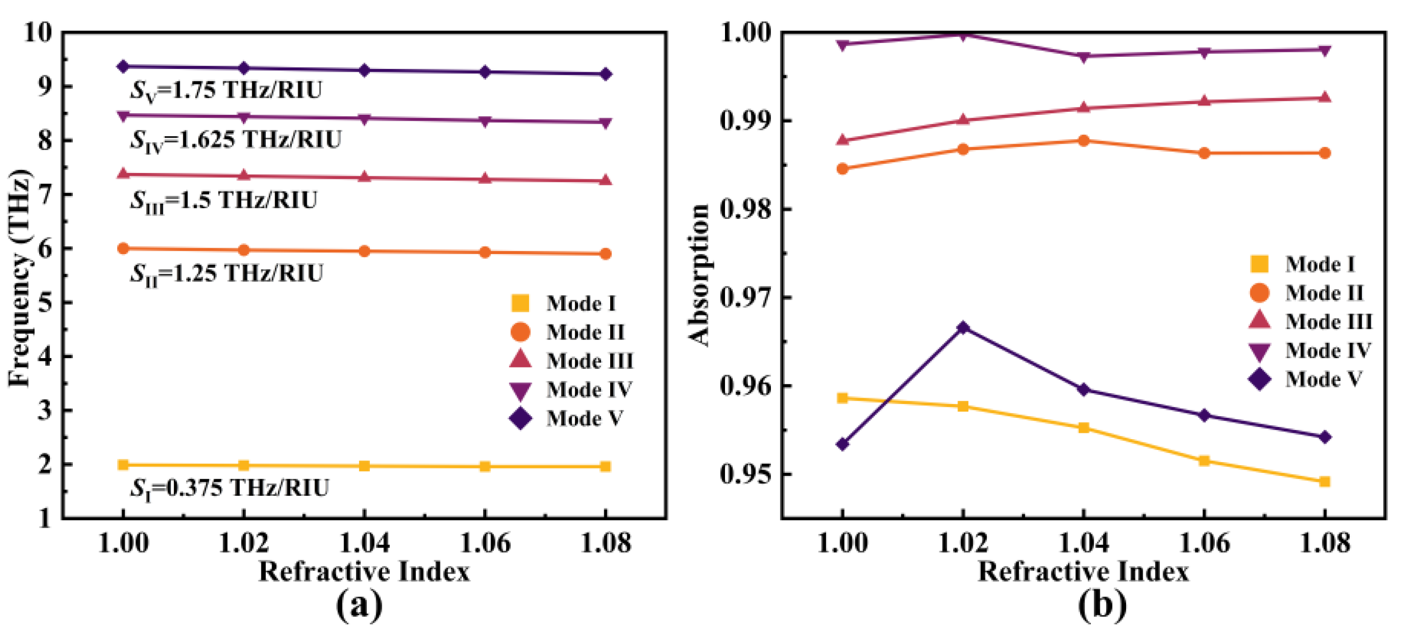
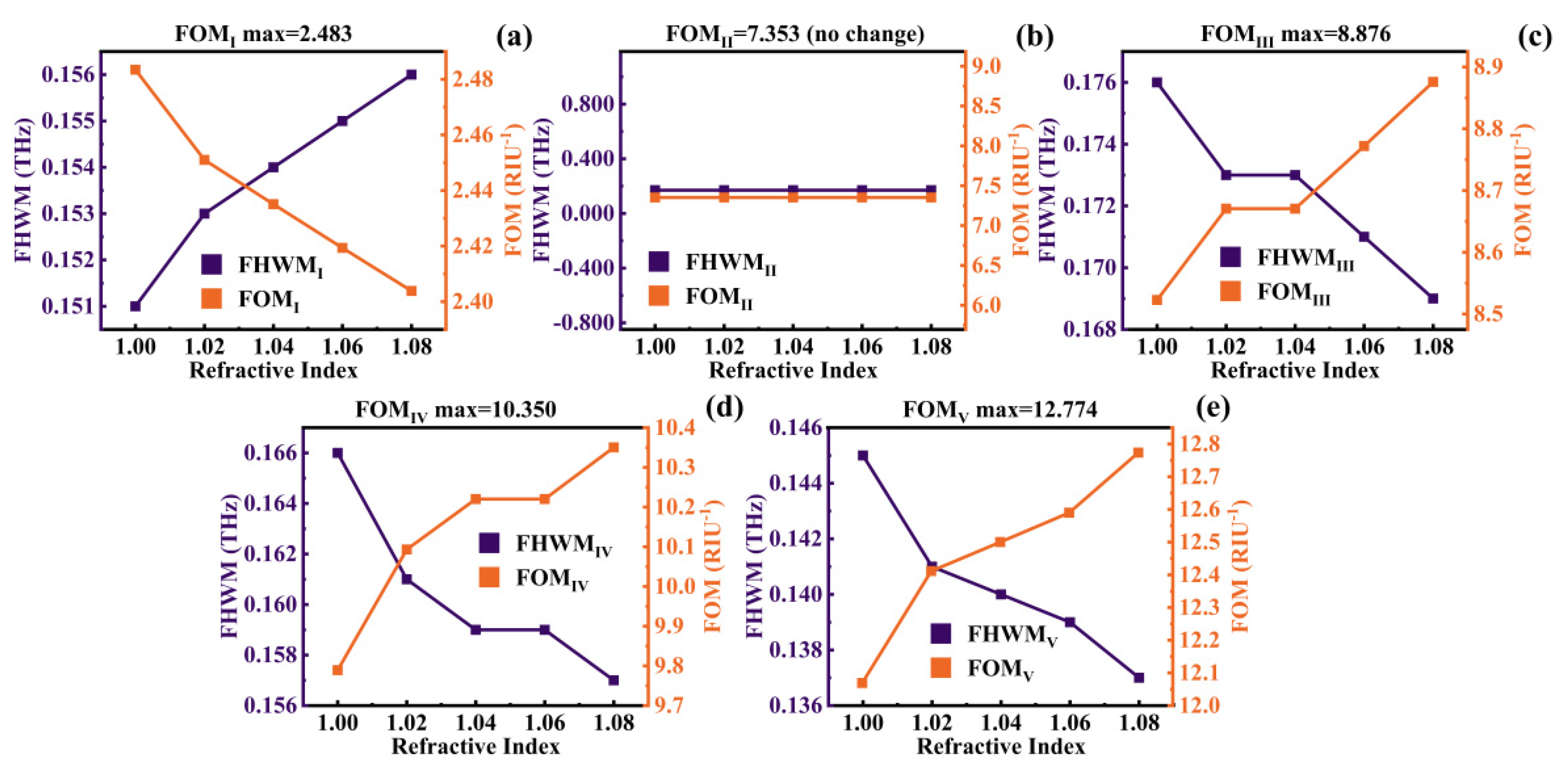
| Mode | I | II | III | IV | V |
|---|---|---|---|---|---|
| FHWMavg (GHz) | 153.8 | 170 | 172.4 | 160.4 | 140.4 |
| FOMavg (RIU−1) | 2.438 | 7.353 | 8.703 | 10.134 | 12.469 |
| Mode | Ⅰ | II | III | IV | V |
|---|---|---|---|---|---|
| FHWMmin (GHz) | 151 | 170 | 169 | 157 | 137 |
| FOMmax (RIU−1) | 2.483 | 7.353 | 8.876 | 10.350 | 12.774 |
Disclaimer/Publisher’s Note: The statements, opinions and data contained in all publications are solely those of the individual author(s) and contributor(s) and not of MDPI and/or the editor(s). MDPI and/or the editor(s) disclaim responsibility for any injury to people or property resulting from any ideas, methods, instructions or products referred to in the content. |
© 2023 by the authors. Licensee MDPI, Basel, Switzerland. This article is an open access article distributed under the terms and conditions of the Creative Commons Attribution (CC BY) license (https://creativecommons.org/licenses/by/4.0/).
Share and Cite
Lai, R.; Chen, H.; Zhou, Z.; Yi, Z.; Tang, B.; Chen, J.; Yi, Y.; Tang, C.; Zhang, J.; Sun, T. Design of a Penta-Band Graphene-Based Terahertz Metamaterial Absorber with Fine Sensing Performance. Micromachines 2023, 14, 1802. https://doi.org/10.3390/mi14091802
Lai R, Chen H, Zhou Z, Yi Z, Tang B, Chen J, Yi Y, Tang C, Zhang J, Sun T. Design of a Penta-Band Graphene-Based Terahertz Metamaterial Absorber with Fine Sensing Performance. Micromachines. 2023; 14(9):1802. https://doi.org/10.3390/mi14091802
Chicago/Turabian StyleLai, Runing, Hao Chen, Zigang Zhou, Zao Yi, Bin Tang, Jing Chen, Yougen Yi, Chaojun Tang, Jianguo Zhang, and Tangyou Sun. 2023. "Design of a Penta-Band Graphene-Based Terahertz Metamaterial Absorber with Fine Sensing Performance" Micromachines 14, no. 9: 1802. https://doi.org/10.3390/mi14091802