

Emerging SiC Applications beyond Power Electronic Devices

 , , , , , and
Abstract
:1. Introduction
2. Results and Discussions
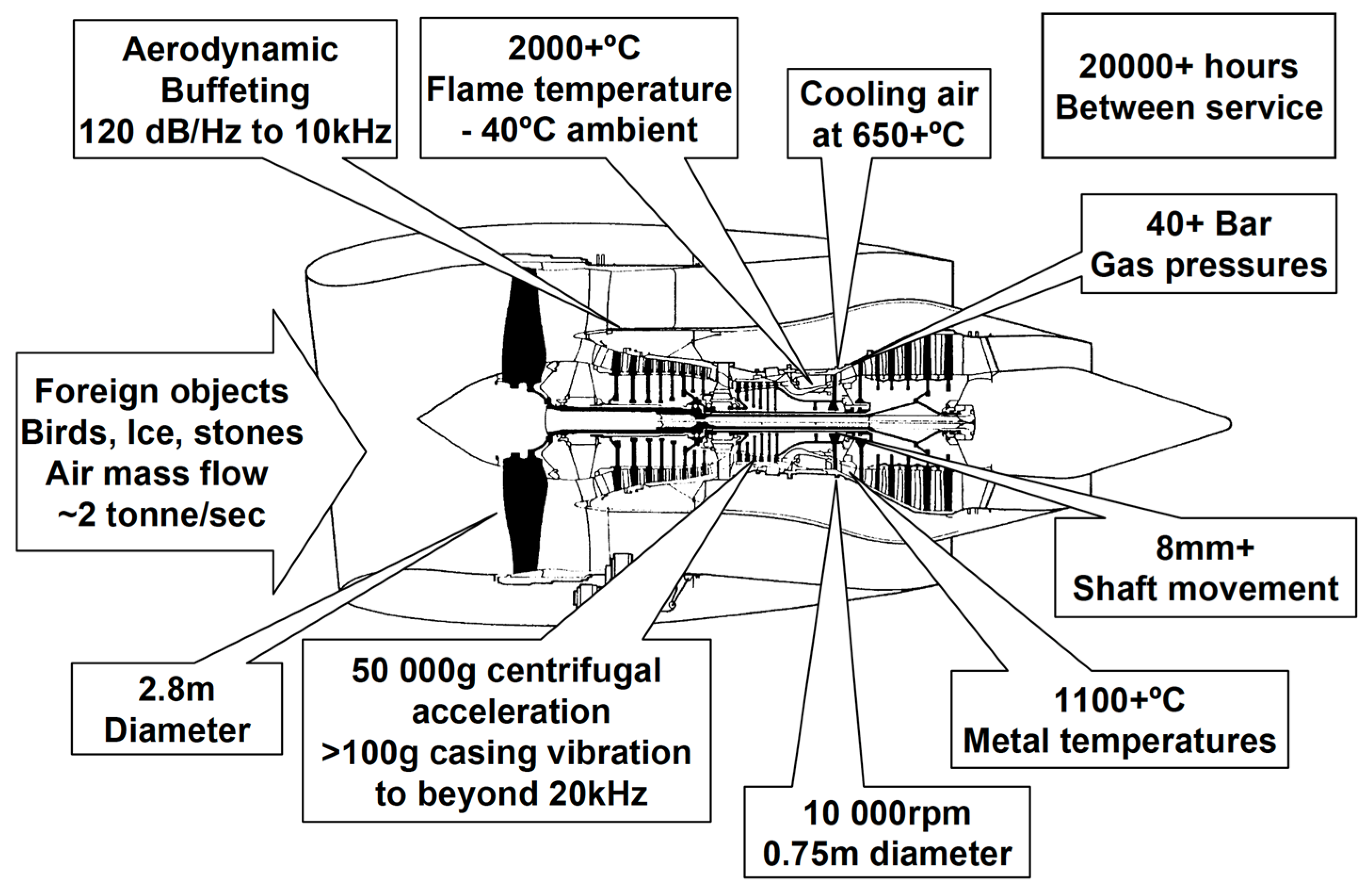
2.1. High Temperature SiC Devices for Aerospace Applications
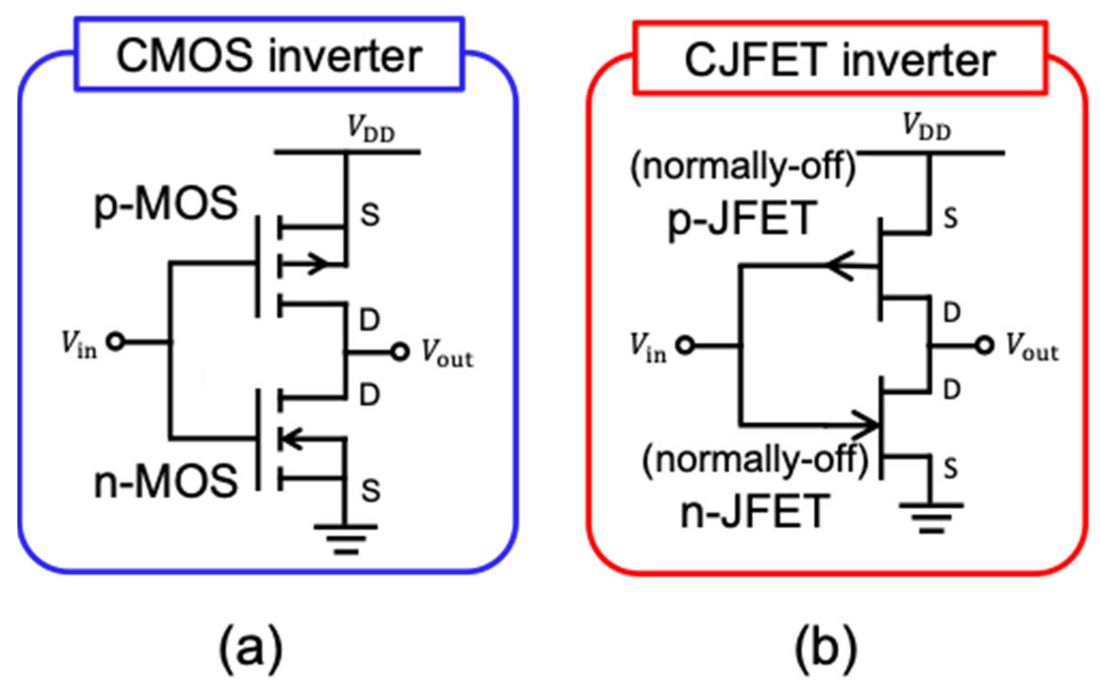
2.2. SiC Complementary MOSFETs and JFETs
2.2.1. Features and Basic Configurations of SiC Complementary FETs
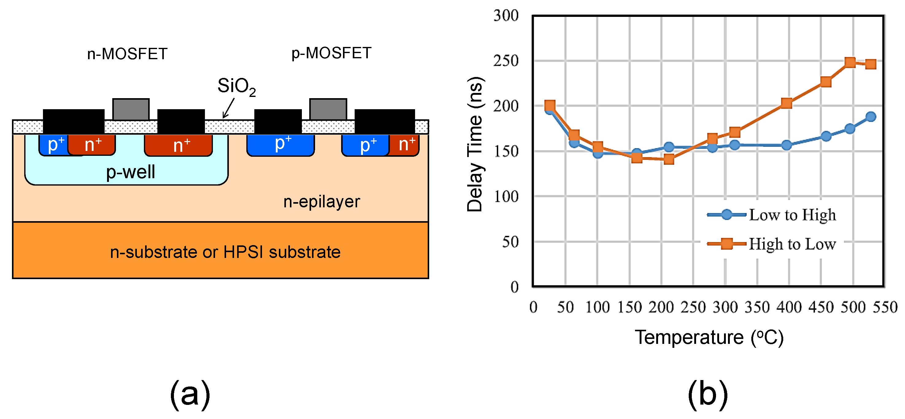
2.2.2. SiC CMOS
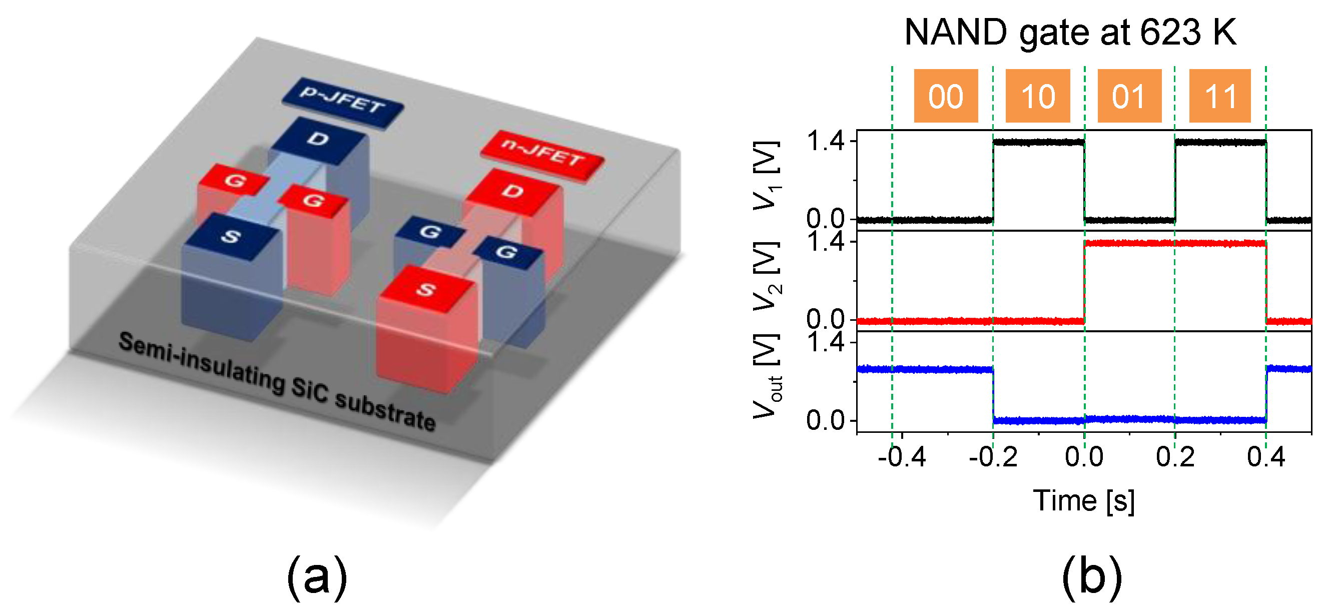
2.2.3. SiC CJFET
2.2.4. Technological Challenges of SiC CMOS and CJFET
3. SiC Detectors
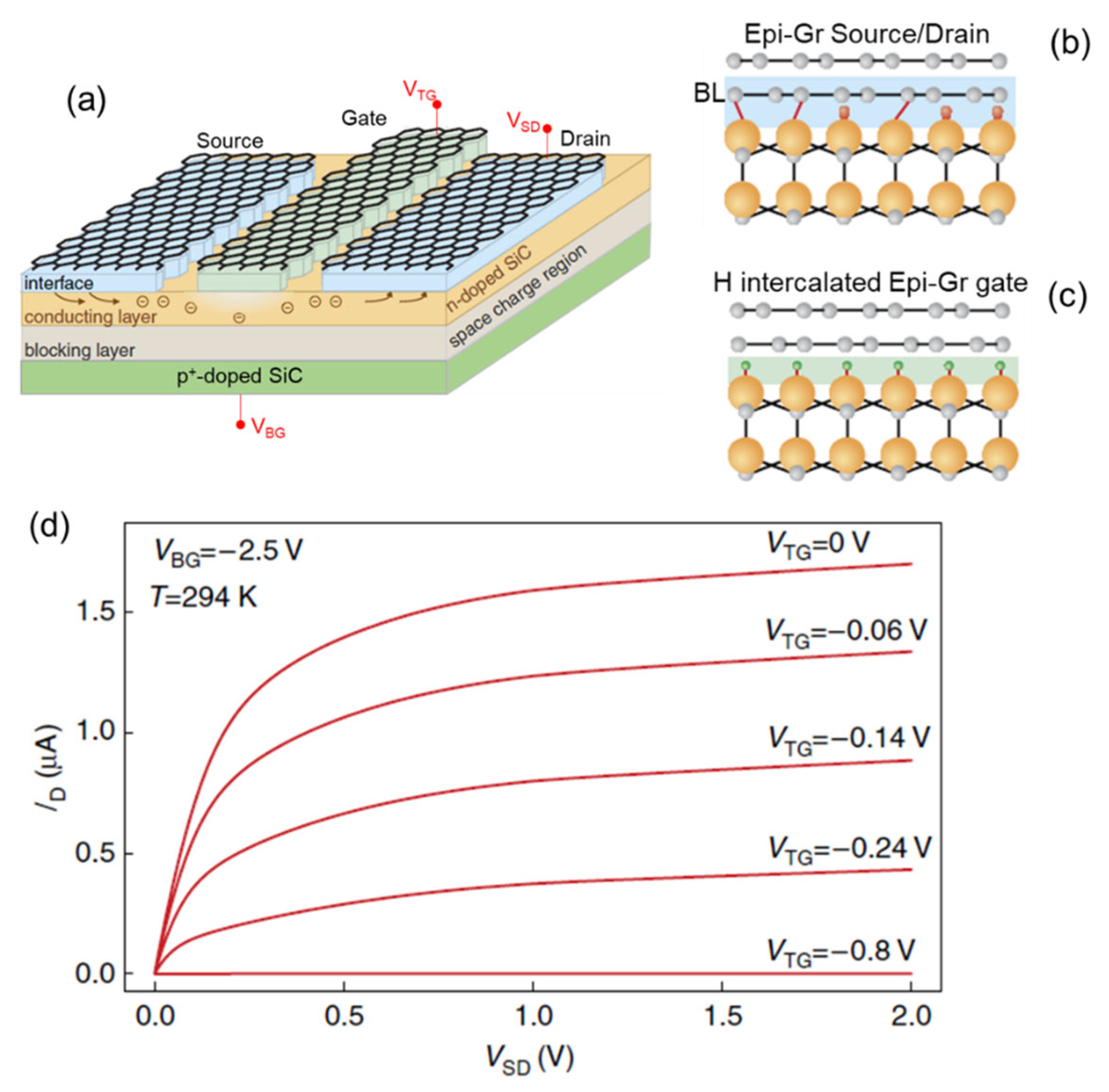
4. 2D Materials’ Integration on Silicon Carbide
5. SiC MEMS
5.1. SiC Material for MEMS
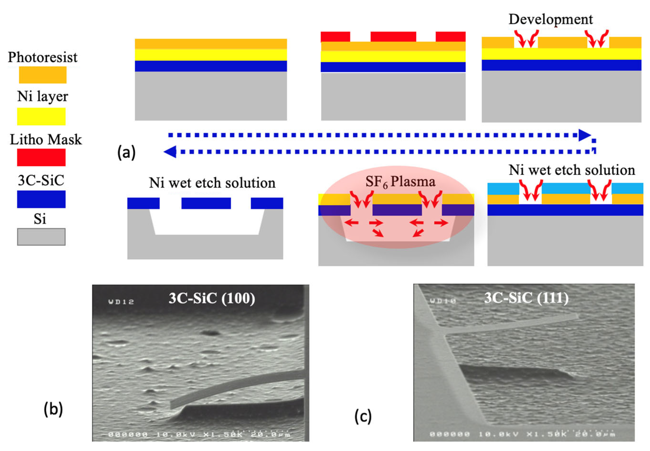
5.2. SiC Micromachining Technologies and Processes
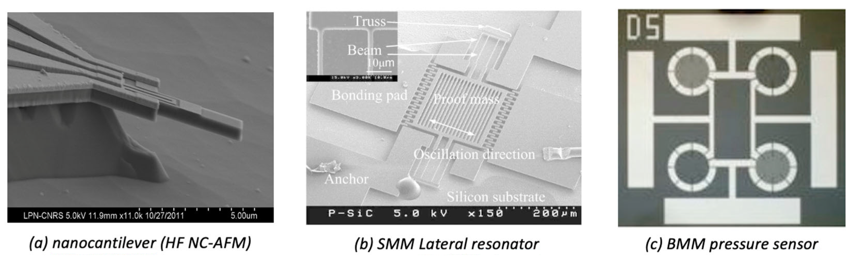
5.3. SiC MEMS Devices
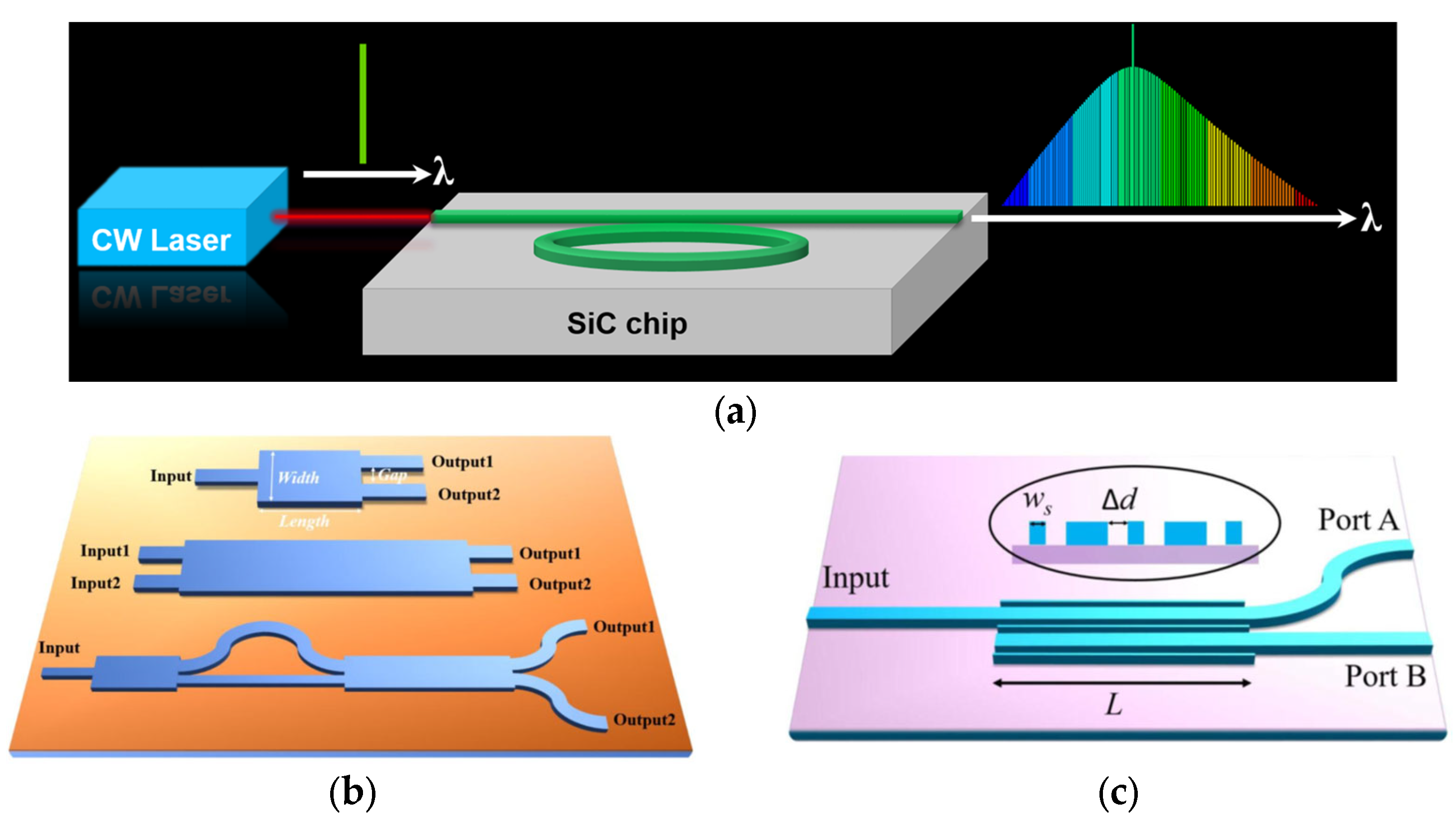
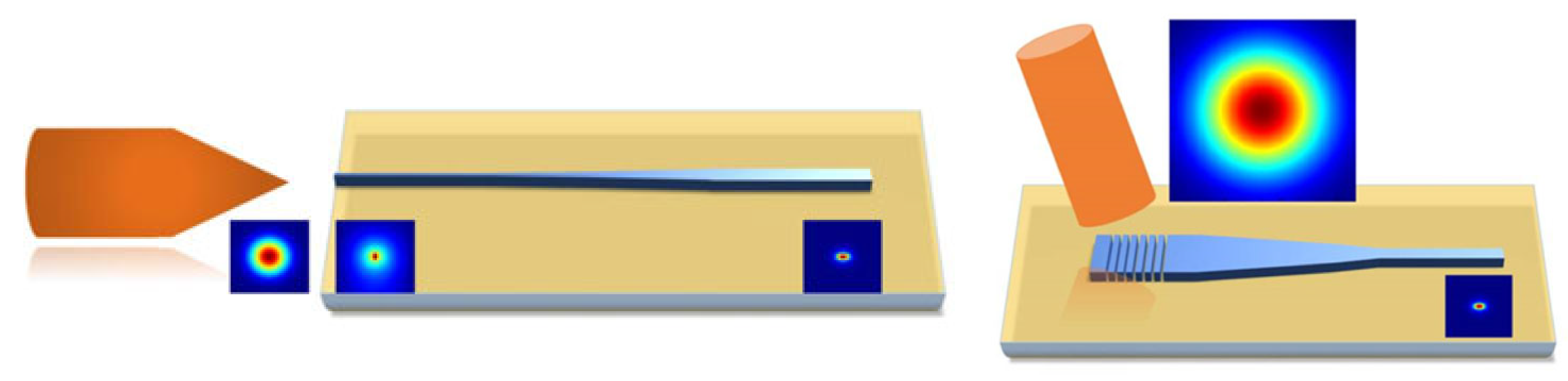
6. SiC Photonic Devices
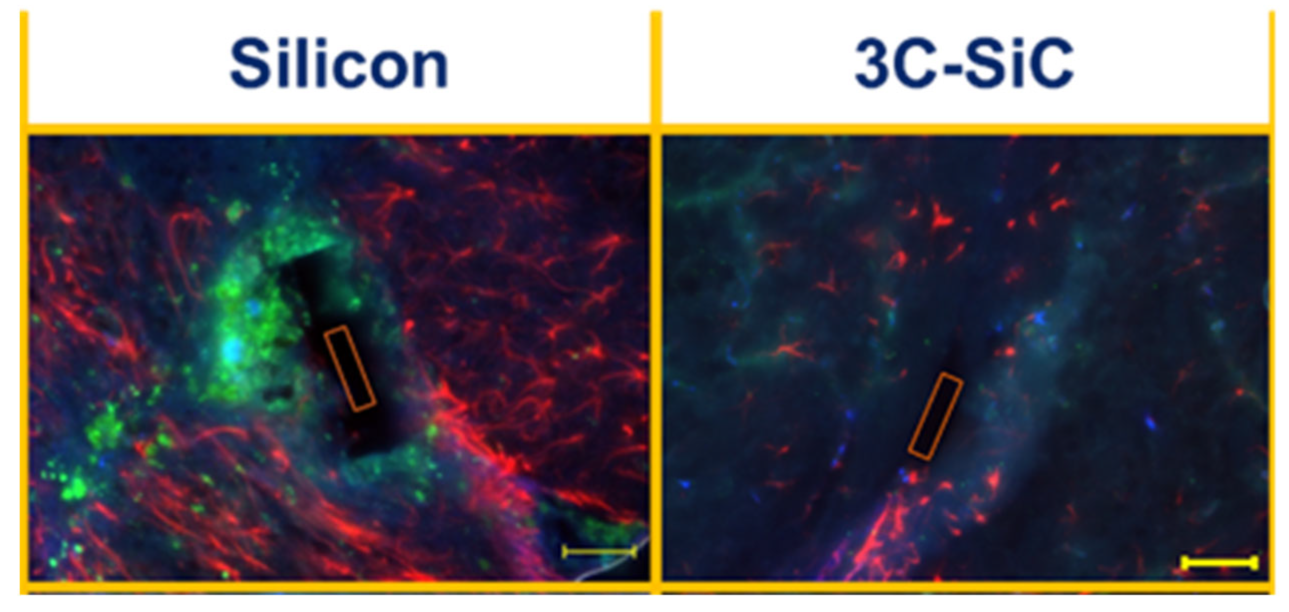
7. Biological Performance of SiC
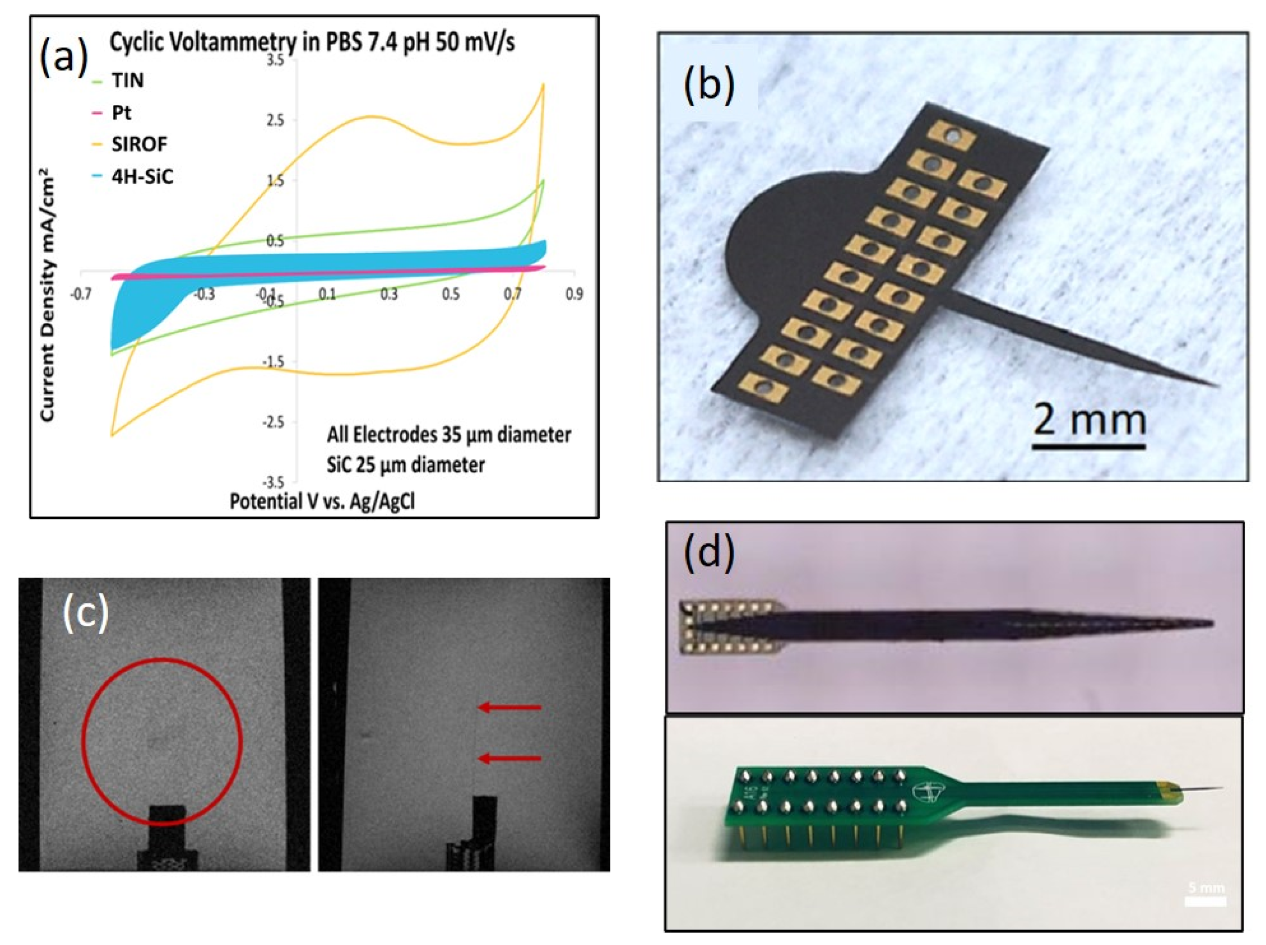
7.1. SiC Biosensors
7.2. SiC Nanotechnology
7.3. SiC Implants
7.4. Bone Scaffolds
8. Conclusions and Outlooks
9. Patents
Author Contributions
Funding
Acknowledgments
Conflicts of Interest
References
- Kimoto, T.; Yonezawa, Y. Current Status and Perspectives of Ultrahigh-Voltage SiC Power Devices. Mater. Sci. Semicond. Process. 2018, 78, 43–56. [Google Scholar] [CrossRef]
- Cooper, J.A.; Agarwal, A. SiC Power-Switching Devices—The Second Electronics Revolution? Proc. IEEE 2002, 90, 956–968. [Google Scholar] [CrossRef]
- Agarwal, A.K. An Overview of SiC Power Devices. In Proceedings of the 2010 International Conference on Power, Control and Embedded Systems, Allahabad, India, 29 November–1 December 2010. [Google Scholar] [CrossRef]
- Kimoto, T. Material Science and Device Physics in SiC Technology for High-Voltage Power Devices. Jpn. J. Appl. Phys. 2015, 54, 040103. [Google Scholar] [CrossRef]
- Okumura, H. Invited Review Paper Present Status and Future Prospect of Widegap Semiconductor High-Power Devices. Jpn. J. Appl. Phys. 2006, 45, 7565–7586. [Google Scholar] [CrossRef] [Green Version]
- La Via, F.; Roccaforte, F.; la Magna, A.; Nipoti, R.; Mancarella, F.; Wellman, P.; Crippa, D.; Mauceri, M.; Ward, P.; Miglio, L.; et al. 3C-SiC Hetero-Epitaxially Grown on Silicon Compliance Substrates and New 3C-SiC Substrates for Sustainable Wide-Band-Gap Power Devices (CHALLENGE). Eur. Comm. 2018, 924, 913–918. [Google Scholar] [CrossRef]
- Sarro, P.M. Silicon Carbide as a New MEMS Technology. Sens. Actuators A Phys. 2000, 82, 210–218. [Google Scholar] [CrossRef]
- Cutroneo, M.; Musumeci, P.; Zimbone, M.; Torrisi, L.; La Via, F.; Margarone, D.; Velyhan, A.; Ullschmied, J.; Calcagno, L. High Performance SiC Detectors for MeV Ion Beams Generated by Intense Pulsed Laser Plasmas. J. Mater. Res. 2013, 28, 87–93. [Google Scholar] [CrossRef]
- Beygi, M.; Bentley, J.T.; Frewin, C.L.; Kuliasha, C.A.; Takshi, A.; Bernardin, E.K.; La Via, F.; Saddow, S.E. Fabrication of a Monolithic Implantable Neural Interface from Cubic Silicon Carbide. Micromachines 2019, 10, 430. [Google Scholar] [CrossRef] [PubMed] [Green Version]
- Han, T.; Privitera, S.; Milazzo, R.G.G.; Bongiorno, C.; Di Franco, S.; La Via, F.; Song, X.; Shi, Y.; Lanza, M.; Lombardo, S.; et al. Materials Science & Engineering B Photo-Electrochemical Water Splitting in Silicon Based Photocathodes Enhanced by Plasmonic/Catalytic Nanostructures. Mater. Sci. Eng. B Solid State Mater. Adv. Technol. 2017, 225, 128–133. [Google Scholar] [CrossRef]
- La Via, F.; Severino, A.; Anzalone, R.; Bongiorno, C.; Litrico, G.; Mauceri, M.; Schoeler, M.; Schuh, P.; Wellmann, P. From Thin Film to Bulk 3C-SiC Growth: Understanding the Mechanism of Defects Reduction. Mater. Sci. Semicond. Process. 2018, 78, 57–68. [Google Scholar] [CrossRef]
- Neudeck, P.; Spry, D.; Krasowski, M.; Chen, L.; Prokop, N.; Greer, L.; Chang, C. Progressing −190 °C to +500 °C Durable SiC JFET ICs From MSI to LSI. In Proceedings of the 2020 IEEE International Electron. Devices Meeting (IEDM), San Francisco, CA, USA, 12–18 December 2020. [Google Scholar] [CrossRef]
- Shakir, M.; Hou, S.; Hedayati, R.; Malm, B.G.; Östling, M.; Zetterling, C.M. Towards Silicon Carbide VLSI Circuits for Extreme Environment Applications. Electronics 2019, 8, 496. [Google Scholar] [CrossRef] [Green Version]
- Taur, Y.; Tak, H. NingFundamentals of Modern VLSI Devices. Google Libri. Available online: https://books.google.it/books?hl=it&lr=&id=cbhIEAAAQBAJ&oi=fnd&pg=PR13&dq=3.%09Taur,+Y.%3B+Ning,+T.+H.+Fundamentals+of+Modern+VLSI+Devices,+3rd+ed.+(Cambridge+Univ.+Press,+2021).&ots=MairrFIxP1&sig=mlzfVcheucs1gHdDxIDjQrZIRso&redir_esc=y#v=onepage&q&f=false (accessed on 6 March 2023).
- Zekentes, K.; Choi, J.; Stambouli, V.; Bano, E.; Karker, O.; Rogdakis, K. Progress in SiC Nanowire Field-Effect-Transistors for Integrated Circuits and Sensing Applications. Microelectron. Eng. 2022, 255, 111704. [Google Scholar] [CrossRef]
- Rogdakis, K.; Lee, S.Y.; Bescond, M.; Lee, S.K.; Bano, E.; Zekentes, K. 3C-Silicon Carbide Nanowire FET: An Experimental and Theoretical Approach. IEEE Trans. Electron. Devices 2008, 55, 1970–1976. [Google Scholar] [CrossRef]
- Peng, G.; Zhou, Y.; He, Y.; Yu, X.; Zhang, X.A.; Li, G.Y.; Haick, H. UV-Induced SiC Nanowire Sensors. J. Phys. D Appl. Phys. 2015, 48, 055102. [Google Scholar] [CrossRef]
- Chen, J.; Zhang, J.; Wang, M.; Li, Y. High-Temperature Hydrogen Sensor Based on Platinum Nanoparticle-Decorated SiC Nanowire Device. Sens. Actuators B Chem. 2014, 201, 402–406. [Google Scholar] [CrossRef]
- Ou, H.; Shi, X.; Lu, Y.; Kollmuss, M.; Steiner, J.; Tabouret, V.; Syväjärvi, M.; Wellmann, P.; Chaussende, D. Novel Photonic Applications of Silicon Carbide. Materials 2023, 16, 1014. [Google Scholar] [CrossRef]
- Castelletto, S.; Peruzzo, A.; Bonato, C.; Johnson, B.C.; Radulaski, M.; Ou, H.; Kaiser, F.; Wrachtrup, J. Silicon Carbide Photonics Bridging Quantum Technology. ACS Photonics 2021, 9, 1434–1457. [Google Scholar] [CrossRef]
- Michaud, J.-F.; Portail, M.; Alquier, D. 3C-SiC—From Electronic to MEMS Devices. In Advanced Silicon Carbide Devices and Processing; IntechOpen: London, UK, 2015. [Google Scholar] [CrossRef] [Green Version]
- Locke, C.; Kravchenko, G.; Waters, P.; Reddy, J.D.; Du, K.; Volinsky, A.A.; Frewin, C.L.; Saddow, S.E. 3C-SiC Films on Si for MEMS Applications: Mechanical Properties. In Proceedings of the Materials Science Forum; Trans Tech Publications Ltd.: Stafa-Zurich, Switzerland, 2009; Volume 615–617, pp. 633–636. [Google Scholar]
- Michaud, J.F.; Zielinski, M.; Ben Messaoud, J.; Chassagne, T.; Portail, M.; Alquier, D. Influence of Aluminum Incorporation on Mechanical Properties of 3C-SiC Epilayers. In Proceedings of the Materials Science Forum; Trans Tech Publications Ltd.: Stafa-Zurich, Switzerland, 2018; Volume 924 MSF, pp. 318–321. [Google Scholar]
- Anzalone, R.; Piluso, N.; Marino, A.; Sciuto, A.; D’Arrigo, G. Very Low Dose Ion-Implantation Effect on Heteroepitaxial 3C-SiC Mechanical Properties. Phys. Status Solidi 2012, 209, 2235–2240. [Google Scholar] [CrossRef]
- Pozzi, M.; Hassan, M.; Harris, A.J.; Burdess, J.S.; Jiang, L.; Lee, K.K.; Cheung, R.; Phelps, G.J.; Wright, N.G.; Zorman, C.A.; et al. Mechanical Properties of a 3C-SiC Film between Room Temperature and 600 °C. J. Phys. D Appl. Phys. 2007, 40, 3335–3342. [Google Scholar] [CrossRef]
- Zhang, J.; Carraro, C.; Howe, R.T.; Maboudian, R. Electrical, Mechanical and Metal Contact Properties of Polycrystalline 3C-SiC Films for MEMS in Harsh Environments. Surf. Coat. Technol. 2007, 201, 8893–8898. [Google Scholar] [CrossRef]
- Modulus, Y.; Anzalone, R.; D’Arrigo, G.; Camarda, M.; Piluso, N.; La Via, F. Evaluation of Mechanical and Optical Properties of Hetero-Epitaxial Single Crystal 3C-SiC Squared-Membrane. Mater. Sci. Forum 2014, 780, 457–460. [Google Scholar] [CrossRef]
- Umeno, Y.; Yagi, K.; Nagasawa, H. Ab Initio Calculation of Mechanical Properties of Stacking Fault in 3C-SiC: Effect of Stress and Doping. Mater. Sci. Forum 2012, 1, 415–418. [Google Scholar] [CrossRef]
- Saddow, S.E. Silicon Carbide Technology for Advanced Human Healthcare Applications. Micromachines 2022, 13, 346. [Google Scholar] [CrossRef] [PubMed]
- Saddow, S.E. Silicon Carbide Biotechnology: A Biocompatible Semiconductor for Advanced Biomedical Devices and Applications, 2nd ed.; Elsevier Inc.: Amsterdam, The Netherlands, 2016; ISBN 9780128029930. [Google Scholar]
- Saddow, S.E. Silicon Carbide Biotechnology: A Biocompatible Semiconductor for Advanced Biomedical Devices and Applications; Elsevier Inc.: Amsterdam, The Netherlands, 2012; p. 479. [Google Scholar]
- Shenai, K.; Scott, R.S.; Baliga, B.J. Optimum Semiconductors for High-Power Electronics. IEEE Trans. Electron. Devices 1989, 36, 1811–1823. [Google Scholar] [CrossRef]
- Garg, S.; Schadow, K.; Horn, W.; Pfoertner, H.; Stiharu, I. Sensor and Actuator Needs for More Intelligent Gas Turbine Engines. Proc. ASME Turbo Expo 2010, 3, 155–167. [Google Scholar] [CrossRef] [Green Version]
- Quigley, R.E. More Electric Aircraft. In Proceedings of the Eighth Annual Applied Power Electronics Conference and Exposition (APEC), San Diego, CA, USA, 7–11 March 1993; pp. 906–911. [Google Scholar] [CrossRef]
- Reinhardt, K.C.; Marciniak, M.A. Wide-Bandgap Power Electronics for the More Electric Aircraft. In Proceedings of the 31st Intersociety Energy Conversion Engineering Conference, Washington, DC, USA, 11–16 August 1996; Volume 1, pp. 127–132. [Google Scholar] [CrossRef]
- Fard, M.T.; He, J.; Huang, H.; Cao, Y. Aircraft Distributed Electric Propulsion Technologies—A Review. IEEE Trans. Transp. Electrif. 2022, 8, 4067–4090. [Google Scholar] [CrossRef]
- Mason, L.S. A Comparison of Energy Conversion Technologies for Space Nuclear Power Systems. In Proceedings of the 2018 International Energy Conversion Engineering Conference, Washington, DC, USA, 9–11 July 2018. [Google Scholar] [CrossRef] [Green Version]
- Kolawa, E.; Mojarradi, M.; del Castillo, L. Extreme Environments in NASA Planetary Exploration. In Extreme Environment Electronics; CRC Press: Boca Raton, FL, USA, 2017; pp. 11–22. [Google Scholar]
- Neudeck, P.G.; Chen, L.; Meredith, R.D.; Lukco, D.; Spry, D.J.; Nakley, L.M.; Hunter, G.W. Operational Testing of 4H-SiC JFET ICs for 60 Days Directly Exposed to Venus Surface Atmospheric Conditions. IEEE J. Electron. Devices Soc. 2019, 7, 140–149. [Google Scholar] [CrossRef]
- Beauchamp, P.; Jessup, K.-L.; Herrick, R.; Kremic, T.; Hunter, G.W. Long-Lived In-Situ Solar System Explorer (LLISSE) Potential Contributions to Solar System Exploration. BAAS 2021, 53, 151. [Google Scholar] [CrossRef]
- Neudeck, P.G.; Spry, D.S.; Krasowski, M.J.; Chang, C.W.; Gonzalez, J.M.; Rajgopal, S.; Prokop, N.F.; Greer, L.C.; Lukco, D.; Maldanado-Rivera, S.; et al. Recent Progress in Extreme Environment Durable SiC JFET-R Integrated Circuit Technology to appear in IMAPSource Proceedings February 2023 (HiTEC). Available online: https://ntrs.nasa.gov/citations/20230002648 (accessed on 27 February 2023).
- Cressler, J.D.; Mantooth, H.A. Extreme Environment Electronics; CRC Press: Boca Raton, FL, USA, 2017; pp. 1–1009. [Google Scholar] [CrossRef]
- Liu, G.; Tuttle, B.R.; Dhar, S. Silicon Carbide: A Unique Platform for Metal-Oxide-Semiconductor Physics. Appl. Phys. Rev. 2015, 2, 021307. [Google Scholar] [CrossRef]
- Kimoto, T.; Watanabe, H. Defect Engineering in SiC Technology for High-Voltage Power Devices. Appl. Phys. Express 2020, 13, 120101. [Google Scholar] [CrossRef]
- Moges, K.; Hosoi, T.; Shimura, T.; Watanabe, H. Demonstration of 4H-SiC CMOS Circuits Consisting of Well-Balanced n- and p-Channel MOSFETs Fabricated by Ultrahigh-Temperature Gate Oxidation. Appl. Phys. Express 2021, 14, 091006. [Google Scholar] [CrossRef]
- Romijn, J.; Vollebregt, S.; Middelburg, L.M.; el Mansouri, B.; van Zeijl, H.W.; May, A.; Erlbacher, T.; Zhang, G.; Sarro, P.M. Integrated Digital and Analog Circuit Blocks in a Scalable Silicon Carbide CMOS Technology. IEEE Trans. Electron. Devices 2022, 69, 4–10. [Google Scholar] [CrossRef]
- Ryu, S.H.; Kornegay, K.T.; Cooper, J.A.; Melloch, M.R. Digital CMOS IC’s in 6H-SiC Operating on a 5-V Power Supply. IEEE Trans. Electron. Devices 1998, 45, 45–53. [Google Scholar] [CrossRef]
- Martin, L.C.; Clark, D.; Ramsay, E.P.; Murphy, A.E.; Thompson, R.F.; Smith, D.A.; Young, R.A.R.; Cormack, J.D.; Wright, N.G.; Horsfall, A.B. Charge Pumping Analysis of Monolithically Fabricated 4H-SiC CMOS Structures. Mater. Sci. Forum 2013, 740–742, 891–894. [Google Scholar] [CrossRef]
- Barlow, M.; Ahmed, S.; Francis, A.M.; Mantooth, H.A. An Integrated SiC CMOS Gate Driver for Power Module Integration. IEEE Trans. Power Electron. 2019, 34, 11191–11198. [Google Scholar] [CrossRef]
- Rahman, A.; Francis, A.M.; Ahmed, S.; Akula, S.K.; Holmes, J.; Mantooth, A. High-Temperature Voltage and Current References in Silicon Carbide CMOS. IEEE Trans. Electron. Devices 2016, 63, 2455–2461. [Google Scholar] [CrossRef]
- Masunaga, M.; Sato, S.; Kuwana, R.; Sugii, N.; Shima, A. 4H-SiC CMOS Transimpedance Amplifier of Gamma-Irradiation Resistance over 1 MGy. IEEE Trans. Electron. Devices 2020, 67, 224–229. [Google Scholar] [CrossRef]
- Romijn, J.; Vollebregt, S.; Middelburg, L.M.; el Mansouri, B.; van Zeijl, H.W.; May, A.; Erlbacher, T.; Leijtens, J.; Zhang, G.; Sarro, P.M. Integrated 64 Pixel UV Image Sensor and Readout in a Silicon Carbide CMOS Technology. Microsyst. Nanoeng. 2022, 8, 1–17. [Google Scholar] [CrossRef]
- Liu, T.; Zhang, H.; Isukapati, S.B.; Ashik, E.; Morgan, A.J.; Lee, B.; Sung, W.; Fayed, A.; White, M.H.; Agarwal, A.K. SPICE Modeling and Circuit Demonstration of a SiC Power IC Technology. IEEE J. Electron. Devices Soc. 2022, 10, 129–138. [Google Scholar] [CrossRef]
- Jiang, J.Y.; Hung, J.C.; Lo, K.M.; Huang, C.F.; Lee, K.Y.; Tsui, B.Y. Demonstration of CMOS Integration with High-Voltage Double-Implanted MOS in 4H-SiC. IEEE Electron. Device Lett. 2021, 42, 78–81. [Google Scholar] [CrossRef]
- Palmour, J.W.; Lipkin, L.A.; Singh, R.; Slater, D.B.; Suvorov, A.V.; Carter, C.H. SiC Device Technology: Remaining Issues. Diam. Relat. Mater. 1997, 6, 1400–1404. [Google Scholar] [CrossRef]
- Okamoto, M.; Yao, A.; Sato, H.; Harada, S. First Demonstration of a Monolithic SiC Power IC Integrating a Vertical MOSFET with a CMOS Gate Buffer. In Proceedings of the 2021 33rd International Symposium on Power Semiconductor Devices and ICs (ISPSD), Nagoya, Japan, 30 May–3 June 2021; pp. 71–74. [Google Scholar] [CrossRef]
- Isukapati, S.B.; Zhang, H.; Liu, T.; Ashik, E.; Lee, B.; Morgan, A.J.; Sung, W.; Fayed, A.; Agarwal, A.K. Monolithic Integration of Lateral HV Power MOSFET with LV CMOS for SiC Power IC Technology. In Proceedings of the 2021 33rd International Symposium on Power Semiconductor Devices and ICs (ISPSD), Nagoya, Japan, 30 May–3 June 2021; pp. 267–270. [Google Scholar] [CrossRef]
- Zuleeg, R.; Notthoff, J.K.; Troeger, G.L. Double-Implanted GaAs Complementary JFET’s. IEEE Electron. Device Lett. 1984, 5, 21–23. [Google Scholar] [CrossRef]
- Habib, H. Complementary JFET Logic in Silicon Carbide; Newcastle University: Newcastle upon Tyne, UK, 2013. [Google Scholar]
- Nakajima, M.; Kaneko, M.; Kimoto, T. Normally-off 400 °C Operation of n- and p-JFETs with a Side-Gate Structure Fabricated by Ion Implantation into a High-Purity Semi-Insulating SiC Substrate. IEEE Electron. Device Lett. 2019, 40, 866–869. [Google Scholar] [CrossRef]
- Kaneko, M.; Nakajima, M.; Jin, Q.; Kimoto, T. SiC Complementary Junction Field-Effect Transistor Logic Gate Operation at 623 K. IEEE Electron. Device Lett. 2022, 43, 997–1000. [Google Scholar] [CrossRef]
- Noborio, M.; Suda, J.; Kimoto, T. P-Channel MOSFETs on 4H-SiC {0001} and Nonbasal Faces Fabricated by Oxide Seposition and Notation N2O Annealing. IEEE Trans. Electron. Devices 2009, 56, 1953–1958. [Google Scholar] [CrossRef]
- Lelis, A.J.; Green, R.; Habersat, D.B.; El, M. Basic Mechanisms of Threshold-Voltage Instability and Implications for Reliability Testing of SiC MOSFETs. IEEE Trans. Electron. Devices 2015, 62, 316–323. [Google Scholar] [CrossRef]
- Yang, L.; Bai, Y.; Li, C.; Chen, H.; Tang, Y.; Hao, J.; Yang, C.; Tian, X.; Lu, J.; Liu, X. Bias Temperature Instability of 4H-SiC p- and n-Channel MOSFETs Induced by Negative Stress at 200 °C. IEEE Trans. Electron. Devices 2022, 69, 3042–3046. [Google Scholar] [CrossRef]
- Tachiki, K.; Ono, T.; Kobayashi, T.; Tanaka, H.; Kimoto, T. Estimation of Threshold Voltage in SiC Short-Channel MOSFETs. IEEE Trans. Electron. Devices 2018, 65, 3077–3080. [Google Scholar] [CrossRef]
- Kaneko, M.; Nakajima, M.; Jin, Q.; Kimoto, T. Experimental Study on Short-Channel Effects in Double-Gate Silicon Carbide JFETs. IEEE Trans. Electron. Devices 2020, 67, 4538–4540. [Google Scholar] [CrossRef]
- Lebedev, A.A. Deep Level Centers in Silicon Carbide: A Review. Semiconductors 1999, 33, 107–130. [Google Scholar] [CrossRef]
- Laref, A.; Laref, S. Electronic and Optical Properties of SiC Polytypes Using a Transferable Semi-Empirical Tight-Binding Model. Phys. Status Solidi B Basic Res. 2008, 245, 89–100. [Google Scholar] [CrossRef]
- Basile, A.F.; Rozen, J.; Williams, J.R.; Feldman, L.C.; Mooney, P.M. Capacitance-Voltage and Deep-Level-Transient Spectroscopy Characterization of Defects near SiO2/SiC Interfaces. J. Appl. Phys. 2011, 109, 64514. [Google Scholar] [CrossRef]
- Nipoti, R.; Ayedh, H.M.; Svensson, B.G. Defects Related to Electrical Doping of 4H-SiC by Ion Implantation. Mater. Sci. Semicond. Process. 2018, 78, 13–21. [Google Scholar] [CrossRef]
- Zvanut, M.E.; Konovalov, V.V.; Wang, H.; Mitchel, W.C.; Mitchell, W.D.; Landis, G. Defect Levels and Types of Point Defects in High-Purity and Vanadium-Doped Semi-Insulating 4H–SiC. J. Appl. Phys. 2004, 96, 5484–5489. [Google Scholar] [CrossRef]
- Izzo, G.; Litrico, G.; Calcagno, L.; Foti, G.; La Via, F. Compensation Effects in 7 MeV C Irradiated N-Doped 4H-SiC. Mater. Sci. Forum 2009, 600–603, 619–622. [Google Scholar] [CrossRef]
- Castaldini, A.; Cavallini, A.; Rigutti, L.; Nava, F.; Ferrero, S.; Giorgis, F. Deep Levels by Proton and Electron Irradiation in 4H–SiC. J. Appl. Phys. 2005, 98, 053706. [Google Scholar] [CrossRef]
- Izzo, G.; Litrico, G.; Severino, A.; Foti, G.; La Via, F.; Calcagno, L. Defects in High Energy Ion Irradiated 4H-SiC. Mater. Sci. Forum 2009, 615–617, 397–400. [Google Scholar] [CrossRef]
- Izzo, G.; Litrico, G.; Calcagno, L.; Foti, G.; La Via, F. Electrical Properties of High Energy Ion Irradiated 4H-SiC Schottky Diodes. J. Appl. Phys. 2008, 104, 093711. [Google Scholar] [CrossRef]
- Moscatelli, F.; Scorzoni, A.; Poggi, A.; Passini, M.; Pizzocchero, G.; Nipoti, R. Effects of Very High Neutron Fluence Irradiation on P+n Junction 4H-SiC Diodes. Mater. Sci. Forum 2007, 556–557, 917–920. [Google Scholar] [CrossRef]
- Raciti, G.; De Napoli, M.; Giacoppo, F.; Rapisarda, E.; Sfienti, C. Detection Properties and Radiation Damage Effects in SiC Diodes Irradiated with Light Ions. Nucl. Phys. A 2010, 834, 784c–787c. [Google Scholar] [CrossRef]
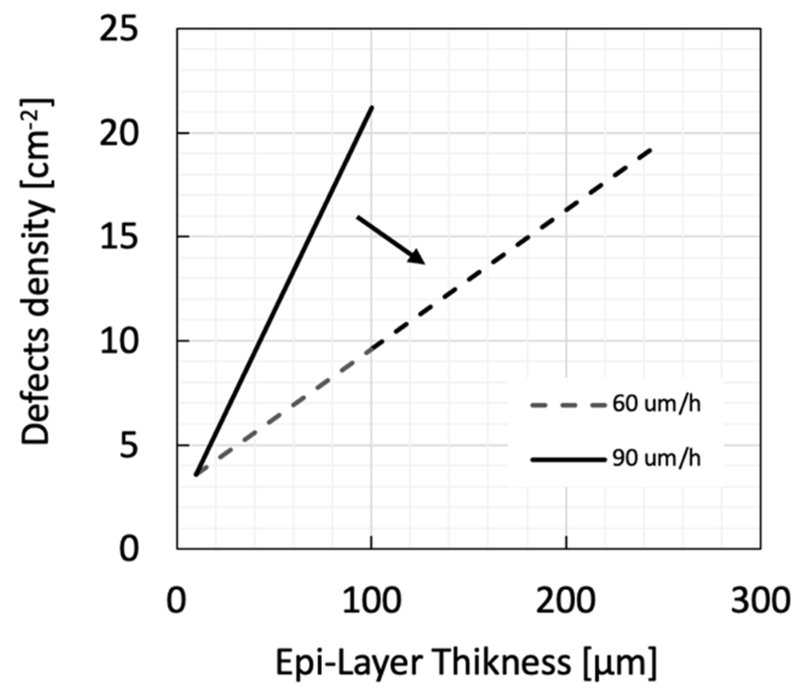
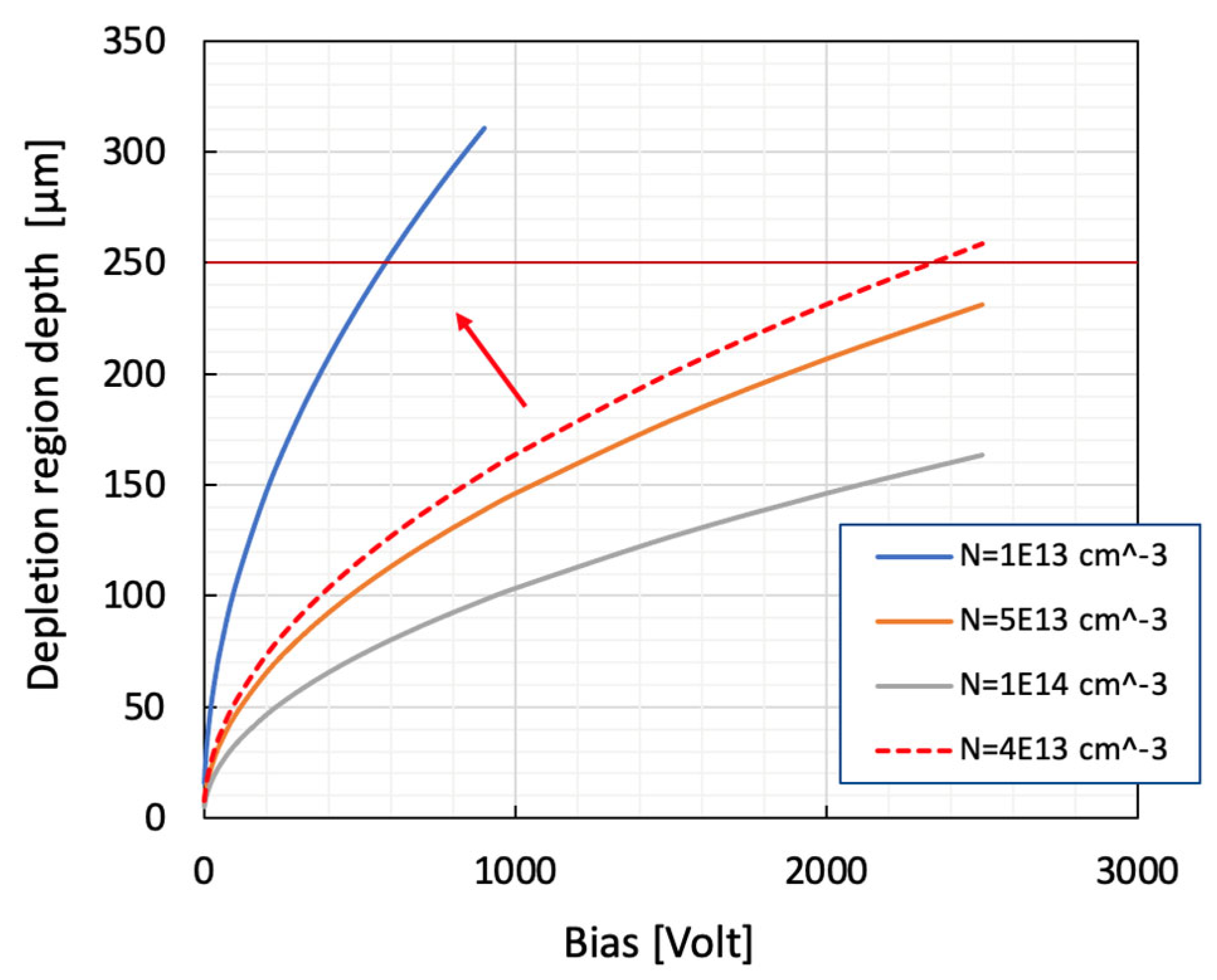
- La Via, F.; Camarda, M.; La Magna, A. Mechanisms of Growth and Defect Properties of Epitaxial SiC. Appl. Phys. Rev. 2014, 1, 031301. [Google Scholar] [CrossRef]
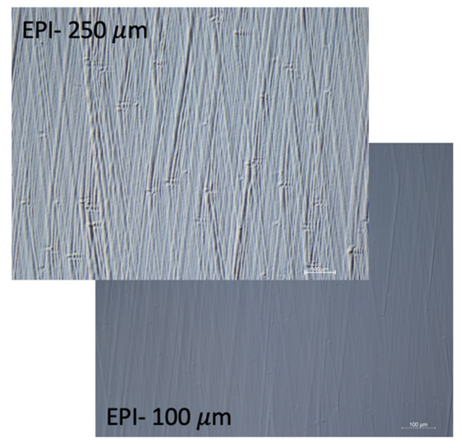
- Mauceri, M.; Pecora, A.; Litrico, G.; Vecchio, C.; Puglisi, M.; Crippa, D.; Piluso, N.; Camarda, M.; La Via, F. 4H-SiC Epitaxial Layer Grown on 150 Mm Automatic Horizontal Hot Wall Reactor PE106. Mater. Sci. Forum 2014, 778, 121–124. [Google Scholar] [CrossRef]
- Meli, A.; Muoio, A.; Reitano, R.; Sangregorio, E.; Calcagno, L.; Trotta, A.; Parisi, M.; Meda, L.; La Via, F. Effect of the Oxidation Process on Carrier Lifetime and on SF Defects of 4H SiC Thick Epilayer for Detection Applications. Micromachines 2022, 13, 1042. [Google Scholar] [CrossRef] [PubMed]
- Altana, C.; Calcagno, L.; Ciampi, C.; La Via, F.; Lanzalone, G.; Muoio, A.; Pasquali, G.; Pellegrino, D.; Puglia, S.; Rapisarda, G.; et al. Study of Radiation Damage Induced by Heavy Ion Beams on Silicon and Silicon Carbide Detectors. Sensors 2023. submitted. [Google Scholar]
- Rebai, M.; Rigamonti, D.; Cancelli, S.; Croci, G.; Gorini, G.; Perelli Cippo, E.; Putignano, O.; Tardocchi, M.; Altana, C.; Angelone, M.; et al. New Thick Silicon Carbide Detectors: Response to 14 MeV Neutrons and Comparison with Single-Crystal Diamonds. Nucl. Instrum. Methods Phys. Res. A 2019, 946, 162637. [Google Scholar] [CrossRef]
- Kushoro, M.H.; Rebai, M.; Tardocchi, M.; Altana, C.; Cazzaniga, C.; De Marchi, E.; La Via, F.; Meda, L.; Meli, A.; Parisi, M.; et al. Detector Response to D-d Neutrons and Stability Measurements with 4h Silicon Carbide Detectors. Materials 2021, 14, 568. [Google Scholar] [CrossRef]
- Nida, S.; Tsibizov, A.; Ziemann, T.; Woerle, J.; Moesch, A.; Schulze-Briese, C.; Pradervand, C.; Tudisco, S.; Sigg, H.; Bunk, O.; et al. Silicon Carbide X-Ray Beam Position Monitors for Synchrotron Applications. J. Synchrotron. Radiat. 2019, 26, 28–35. [Google Scholar] [CrossRef] [Green Version]
- Tudisco, S.; Altana, C.; Boscardin, M.; Calcagno, L.; Ciampi, C.; Cirrone, G.A.P.; Fazzi, A.; Giove, D.; Gorini, G.; Labate, L.; et al. Silicon Carbide for Future Intense Luminosity Nuclear Physics Investigations. Nuovo Cim. Soc. Ital. Fis. C 2019, 42, i2019–i19074. [Google Scholar]
- Ciampi, C.; Pasquali, G.; Altana, C.; Bini, M.; Boscardin, M.; Calcagno, L.; Casini, G.; Cirrone, G.A.P.; Fazzi, A.; Labate, L.; et al. Nuclear Fragment Identification with E-E Telescopes Exploiting Silicon Carbide Detectors SiCILIA Collaboration. Nucl. Inst. Methods Phys. Res. A 2019, 925, 60–69. [Google Scholar] [CrossRef]
- Jariwala, D.; Marks, T.J.; Hersam, M.C. Mixed-Dimensional van Der Waals Heterostructures. Nat. Mater. 2016, 16, 170–181. [Google Scholar] [CrossRef] [Green Version]
- Ruhl, G.; Wittmann, S.; Koenig, M.; Neumaier, D. The Integration of Graphene into Microelectronic Devices. Beilstein J. Nanotechnol. 2017, 8, 1056–1064. [Google Scholar] [CrossRef] [PubMed]
- Giannazzo, F.; Fisichella, G.; Greco, G.; La Magna, A.; Roccaforte, F.; Pecz, B.; Yakimova, R.; Dagher, R.; Michon, A.; Cordier, Y. Graphene Integration with Nitride Semiconductors for High Power and High Frequency Electronics. Phys. Status Solidi 2017, 214, 1600460. [Google Scholar] [CrossRef]
- Giannazzo, F.; Deretzis, I.; La Magna, A.; Nicotra, G.; Spinella, C.; Roccaforte, F.; Yakimova, R. Nanoscale Electrical and Structural Properties of Epitaxial Graphene Interface with Sic(0001). In Epitaxial Graphene on Silicon Carbide; Jenny Stanford Publishing: Dubai, United Arab Emirates, 2018; pp. 111–141. [Google Scholar] [CrossRef]
- Lee, E.W.; Ma, L.; Nath, D.N.; Lee, C.H.; Arehart, A.; Wu, Y.; Rajan, S. Growth and Electrical Characterization of Two-Dimensional Layered MoS2/SiC Heterojunctions. Appl. Phys. Lett. 2014, 105, 203504. [Google Scholar] [CrossRef]
- Majety, S.; Li, J.; Zhao, W.P.; Huang, B.; Wei, S.H.; Lin, J.Y.; Jiang, H.X. Hexagonal Boron Nitride and 6H-SiC Heterostructures. Appl. Phys. Lett. 2013, 102, 213505. [Google Scholar] [CrossRef]
- Berger, C.; Song, Z.; Li, X.; Wu, X.; Brown, N.; Naud, C.; Mayou, D.; Li, T.; Hass, J.; Marchenkov, A.N.; et al. Electronic Confinement and Coherence in Patterned Epitaxial Graphene. Science 2006, 312, 1191–1196. [Google Scholar] [CrossRef] [Green Version]
- Emtsev, K.V.; Bostwick, A.; Horn, K.; Jobst, J.; Kellogg, G.L.; Ley, L.; McChesney, J.L.; Ohta, T.; Reshanov, S.A.; Röhrl, J.; et al. Towards Wafer-Size Graphene Layers by Atmospheric Pressure Graphitization of Silicon Carbide. Nat. Mater. 2009, 8, 203–207. [Google Scholar] [CrossRef] [Green Version]
- Virojanadara, C.; Syväjarvi, M.; Yakimova, R.; Johansson, L.I.; Zakharov, A.A.; Balasubramanian, T. Homogeneous Large-Area Graphene Layer Growth on 6H-SiC(0001). Phys. Rev. B Condens. Matter Mater. Phys. 2008, 78, 245403. [Google Scholar] [CrossRef]
- Suemitsu, M.; Jiao, S.; Fukidome, H.; Tateno, Y.; Makabe, I.; Nakabayashi, T. Epitaxial Graphene Formation on 3C-SiC/Si Thin Films. J. Phys. D Appl. Phys. 2014, 47, 094016. [Google Scholar] [CrossRef]
- La Via, F.; Zimbone, M.; Bongiorno, C.; La Magna, A.; Fisicaro, G.; Deretzis, I.; Scuderi, V.; Calabretta, C.; Giannazzo, F.; Zielinski, M.; et al. New Approaches and Understandings in the Growth of Cubic Silicon Carbide. Materials 2021, 14, 5348. [Google Scholar] [CrossRef]
- Giannazzo, F.; Deretzis, I.; La Magna, A.; Roccaforte, F.; Yakimova, R. Electronic Transport at Monolayer-Bilayer Junctions in Epitaxial Graphene on SiC. Phys. Rev. B Condens. Matter Mater. Phys. 2012, 86, 235422. [Google Scholar] [CrossRef]
- Emtsev, K.V.; Speck, F.; Seyller, T.; Ley, L.; Riley, J.D. Interaction, Growth, and Ordering of Epitaxial Graphene on SiC{0001} Surfaces: A Comparative Photoelectron Spectroscopy Study. Phys. Rev. B Condens. Matter Mater. Phys. 2008, 77, 155303. [Google Scholar] [CrossRef] [Green Version]
- Hiebel, F.; Mallet, P.; Varchon, F.; Magaud, L.; Veuillen, J.Y. Graphene-Substrate Interaction on 6H-SiC(000): A Scanning Tunneling Microscopy Study. Phys. Rev. B Condens. Matter Mater. Phys. 2008, 78, 153412. [Google Scholar] [CrossRef]
- Jabakhanji, B.; Camara, N.; Caboni, A.; Consejo, C.; Jouault, B.; Godignon, P.; Camassel, J. Almost Free Standing Graphene on SiC(000-1) and SiC(11-20). Mater. Sci. Forum 2012, 711, 235–241. [Google Scholar] [CrossRef]
- Ostler, M.; Deretzis, I.; Mammadov, S.; Giannazzo, F.; Nicotra, G.; Spinella, C.; Seyller, T.; La Magna, A. Direct Growth of Quasi-Free-Standing Epitaxial Graphene on Nonpolar SiC Surfaces. Phys. Rev. B Condens. Matter Mater. Phys. 2013, 88, 085408. [Google Scholar] [CrossRef] [Green Version]
- Giannazzo, F.; Deretzis, I.; Nicotra, G.; Fisichella, G.; Spinella, C.; Roccaforte, F.; La Magna, A. Electronic Properties of Epitaxial Graphene Residing on SiC Facets Probed by Conductive Atomic Force Microscopy. Appl. Surf. Sci. 2014, 291, 53–57. [Google Scholar] [CrossRef]
- Nicotra, G.; Ramasse, Q.M.; Deretzis, I.; La Magna, A.; Spinella, C.; Giannazzo, F. Delaminated Graphene at Silicon Carbide Facets: Atomic Scale Imaging and Spectroscopy. ACS Nano 2013, 7, 3045–3052. [Google Scholar] [CrossRef]
- Bouhafs, C.; Zakharov, A.A.; Ivanov, I.G.; Giannazzo, F.; Eriksson, J.; Stanishev, V.; Kühne, P.; Iakimov, T.; Hofmann, T.; Schubert, M.; et al. Multi-Scale Investigation of Interface Properties, Stacking Order and Decoupling of Few Layer Graphene on C-Face 4H-SiC. Carbon 2017, 116, 722–732. [Google Scholar] [CrossRef] [Green Version]
- Nicotra, G.; Deretzis, I.; Scuderi, M.; Spinella, C.; Longo, P.; Yakimova, R.; Giannazzo, F.; La Magna, A. Interface Disorder Probed at the Atomic Scale for Graphene Grown on the C Face of SiC. Phys. Rev. B Condens. Matter Mater. Phys. 2015, 91, 155411. [Google Scholar] [CrossRef] [Green Version]
- Varchon, F.; Feng, R.; Hass, J.; Li, X.; Nguyen, B.N.; Naud, C.; Mallet, P.; Veuillen, J.Y.; Berger, C.; Conrad, E.H.; et al. Electronic Structure of Epitaxial Graphene Layers on SiC: Effect of the Substrate. Phys. Rev. Lett. 2007, 99, 126805. [Google Scholar] [CrossRef] [Green Version]
- Sonde, S.; Giannazzo, F.; Raineri, V.; Yakimova, R.; Huntzinger, J.R.; Tiberj, A.; Camassel, J. Electrical Properties of the Graphene/4H-SiC (0001) Interface Probed by Scanning Current Spectroscopy. Phys. Rev. B Condens. Matter Mater. Phys. 2009, 80, 241406. [Google Scholar] [CrossRef]
- Briggs, N.; Gebeyehu, Z.M.; Vera, A.; Zhao, T.; Wang, K.; De La Fuente Duran, A.; Bersch, B.; Bowen, T.; Knappenberger, K.L.; Robinson, J.A. Epitaxial Graphene/Silicon Carbide Intercalation: A Minireview on Graphene Modulation and Unique 2D Materials. Nanoscale 2019, 11, 15440–15447. [Google Scholar] [CrossRef] [PubMed]
- Riedl, C.; Coletti, C.; Iwasaki, T.; Zakharov, A.A.; Starke, U. Quasi-Free-Standing Epitaxial Graphene on SiC Obtained by Hydrogen Intercalation. Phys. Rev. Lett. 2009, 103, 246804. [Google Scholar] [CrossRef] [PubMed] [Green Version]
- Hertel, S.; Waldmann, D.; Jobst, J.; Albert, A.; Albrecht, M.; Reshanov, S.; Schöner, A.; Krieger, M.; Weber, H.B. Tailoring the Graphene/Silicon Carbide Interface for Monolithic Wafer-Scale Electronics. Nat. Commun. 2012, 3, 957. [Google Scholar] [CrossRef] [PubMed] [Green Version]
- Moon, J.S.; Curtis, D.; Hu, M.; Wong, D.; McGuire, C.; Campbell, P.M.; Jernigan, G.; Tedesco, J.L.; VanMil, B.; Myers-Ward, R.; et al. Epitaxial-Graphene RF Field-Effect Transistors on Si-Face 6H-SiC Substrates. IEEE Electron. Device Lett. 2009, 30, 650–652. [Google Scholar] [CrossRef]
- Lin, Y.M.; Dimitrakopoulos, C.; Jenkins, K.A.; Farmer, D.B.; Chiu, H.Y.; Grill, A.; Avouris, P. 100-GHz Transistors from Wafer-Scale Epitaxial Graphene. Science 2010, 327, 662. [Google Scholar] [CrossRef] [Green Version]
- Tzalenchuk, A.; Lara-Avila, S.; Kalaboukhov, A.; Paolillo, S.; Syväjärvi, M.; Yakimova, R.; Kazakova, O.; Janssen, T.J.B.M.; Fal’Ko, V.; Kubatkin, S. Towards a Quantum Resistance Standard Based on Epitaxial Graphene. Nat. Nanotechnol. 2010, 5, 186–189. [Google Scholar] [CrossRef]
- Ribeiro-Palau, R.; Lafont, F.; Brun-Picard, J.; Kazazis, D.; Michon, A.; Cheynis, F.; Couturaud, O.; Consejo, C.; Jouault, B.; Poirier, W.; et al. Quantum Hall Resistance Standard in Graphene Devices under Relaxed Experimental Conditions. Nat. Nanotechnol. 2015, 10, 965–971. [Google Scholar] [CrossRef] [Green Version]
- Pearce, R.; Iakimov, T.; Andersson, M.; Hultman, L.; Spetz, A.L.; Yakimova, R. Epitaxially Grown Graphene Based Gas Sensors for Ultra Sensitive NO2 Detection. Sens. Actuators B. Chem. 2011, 155, 451–455. [Google Scholar] [CrossRef] [Green Version]
- Melios, C.; Panchal, V.; Edmonds, K.; Lartsev, A.; Yakimova, R.; Kazakova, O. Detection of Ultralow Concentration NO2 in Complex Environment Using Epitaxial Graphene Sensors. ACS Sens. 2018, 3, 1666–1674. [Google Scholar] [CrossRef] [Green Version]
- Tehrani, Z.; Burwell, G.; Mohd Azmi, M.A.; Castaing, A.; Rickman, R.; Almarashi, J.; Dunstan, P.; Miran Beigi, A.; Doak, S.H.; Guy, O.J. Generic Epitaxial Graphene Biosensors for Ultrasensitive Detection of Cancer Risk Biomarker. 2D Mater. 2014, 1, 025004. [Google Scholar] [CrossRef]
- Teixeira, S.; Burwell, G.; Castaing, A.; Gonzalez, D.; Conlan, R.S.; Guy, O.J. Epitaxial Graphene Immunosensor for Human Chorionic Gonadotropin. Sens. Actuators B Chem. 2014, 190, 723–729. [Google Scholar] [CrossRef] [Green Version]
- Yang, J.; Guo, L.; Guo, Y.; Hu, W.; Zhang, Z. Epitaxial Graphene/SiC Schottky Ultraviolet Photodiode with Orders of Magnitude Adjustability in Responsivity and Response Speed. Appl. Phys. Lett. 2018, 112, 103501. [Google Scholar] [CrossRef]
- Kuşdemir, E.; Özkendir, D.; Firat, V.; Çelebi, C. Epitaxial Graphene Contact Electrode for Silicon Carbide Based Ultraviolet Photodetector. J. Phys. D Appl. Phys. 2015, 48, 095104. [Google Scholar] [CrossRef]
- Wang, Q.H.; Kalantar-Zadeh, K.; Kis, A.; Coleman, J.N.; Strano, M.S. Electronics and Optoelectronics of Two-Dimensional Transition Metal Dichalcogenides. Nat. Nanotechnol. 2012, 7, 699–712. [Google Scholar] [CrossRef] [PubMed]
- Xiao, Y.; Min, L.; Liu, X.; Liu, W.; Younis, U.; Peng, T.; Kang, X.; Wu, X.; Ding, S.; Zhang, D.W. Facile Integration of MoS2/SiC Photodetector by Direct Chemical Vapor Deposition. Nanophotonics 2020, 9, 3035–3044. [Google Scholar] [CrossRef] [Green Version]
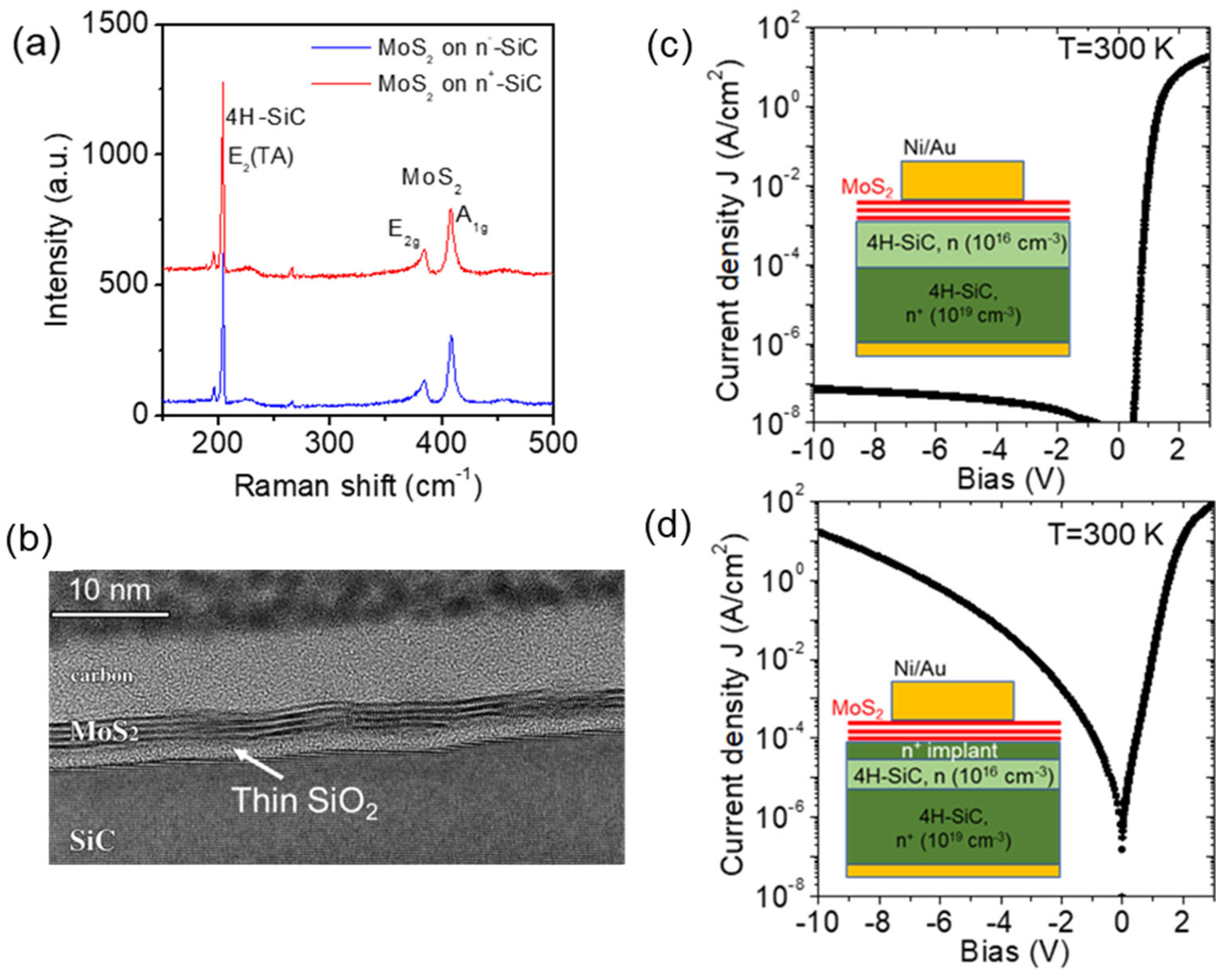
- Giannazzo, F.; Panasci, S.E.; Schilirò, E.; Roccaforte, F.; Koos, A.; Nemeth, M.; Pécz, B. Esaki Diode Behavior in Highly Uniform MoS2/Silicon Carbide Heterojunctions. Adv. Mater. Interfaces 2022, 9, 2200915. [Google Scholar] [CrossRef]
- Giannazzo, F.; Panasci, S.E.; Schilirò, E.; Fiorenza, P.; Greco, G.; Roccaforte, F.; Cannas, M.; Agnello, S.; Koos, A.; Pécz, B.; et al. Highly Homogeneous 2D/3D Heterojunction Diodes by Pulsed Laser Deposition of MoS2 on Ion Implantation Doped 4H-SiC. Adv. Mater. Interfaces 2023, 10, 2201502. [Google Scholar] [CrossRef]
- Serrao, C.R.; Diamond, A.M.; Hsu, S.L.; You, L.; Gadgil, S.; Clarkson, J.; Carraro, C.; Maboudian, R.; Hu, C.; Salahuddin, S. Highly Crystalline MoS2 Thin Films Grown by Pulsed Laser Deposition. Appl. Phys. Lett. 2015, 106, 052101. [Google Scholar] [CrossRef]
- Mehregany, M.; Zorman, C.A. SiC MEMS: Opportunities and Challenges for Applications in Harsh Environments. Thin Solid Films 1999, 356, 518–524. [Google Scholar] [CrossRef]
- Saddow, S.E.; Frewin, C.; Reyes, M.; Register, J.; Nezafati, M.; Thomas, S. 3C-SiC on Si: A Biocompatible Material for Advanced Bioelectronic Devices. ECS Trans. 2014, 61, 101–111. [Google Scholar] [CrossRef]
- Neudeck, P.G. Silicon Carbide Electronic Devices. Encycl. Mater. Sci. Technol. 2001, v, 8508–8519. [Google Scholar] [CrossRef]
- Blevins, J.D. Development of a World Class Silicon Carbide Substrate Manufacturing Capability. IEEE Trans. Semicond. Manuf. 2020, 33, 539–545. [Google Scholar] [CrossRef]
- Zorman, C.A.; Fleischman, A.J.; Dewa, A.S.; Mehregany, M.; Jacob, C.; Nishino, S.; Pirouz, P. Epitaxial Growth of 3C–SiC Films on 4 in. Diam (100) Silicon Wafers by Atmospheric Pressure Chemical Vapor Deposition. J. Appl. Phys. 1998, 78, 5136. [Google Scholar] [CrossRef]
- Nishino, S.; Suhara, H.; Ono, H.; Matsunami, H. Epitaxial Growth and Electric Characteristics of Cubic SiC on Silicon. J. Appl. Phys. 1998, 61, 4889. [Google Scholar] [CrossRef]
- Ferro, G.; Monteil, Y.; Vincent, H.; Thevenot, V.; Tran, M.D.; Cauwet, F.; Bouix, J. Atomic Force Microscopy Growth Modeling of SiC Buffer Layers on Si(100) and Quality Optimization. J. Appl. Phys. 1998, 80, 4691. [Google Scholar] [CrossRef]
- Portail, M.; Zielinski, M.; Chassagne, T.; Roy, S.; Nemoz, M. Comparative Study of the Role of the Nucleation Stage on the Final Crystalline Quality of (111) and (100) Silicon Carbide Films Deposited on Silicon Substrates. J. Appl. Phys. 2009, 105, 083505. [Google Scholar] [CrossRef]
- Pirouz, P.; Chorey, C.M.; Powell, J.A. Antiphase Boundaries in Epitaxially Grown Β-SiC. Appl. Phys. Lett. 1998, 50, 221. [Google Scholar] [CrossRef]
- Yagi, K.; Nagasawa, H. Crystallinity of 3C-SiC Films Grown on Si Substrates. Mater. Sci. Forum 1998, 264–268, 191–194. [Google Scholar] [CrossRef]
- Anzalone, R.; Bongiorno, C.; Severino, A.; D’Arrigo, G.; Abbondanza, G.; Foti, G.; La Via, F. Heteroepitaxial Growth of (111) 3C-SiC on (110) Si Substrate by Second Order Twins. Appl. Phys. Lett. 2008, 92, 224102. [Google Scholar] [CrossRef]
- Locke, C.W.; Severino, A.; La Via, F.; Reyes, M.; Register, J.; Saddow, S.E. SiC Films and Coatings: Amorphous, Polycrystalline, and Single Crystal Forms. In Silicon Carbide Biotechnology: A Biocompatible Semiconductor for Advanced Biomedical Devices and Applications; Elsevier Inc.: Amsterdam, The Netherlands, 2012; Chapter 2; pp. 17–61. [Google Scholar] [CrossRef]
- Du, J.; Singh, N.; Summers, J.B.; Zorman, C.A. Development of PECVD SiC for MEMS Using 3MS as the Precursor. Mater. Res. Soc. Symp. Proc. 2006, 911, 283–288. [Google Scholar] [CrossRef]
- Ovanesyan, R.A.; Filatova, E.A.; Elliott, S.D.; Hausmann, D.M.; Smith, D.C.; Agarwal, S. Atomic Layer Deposition of Silicon-Based Dielectrics for Semiconductor Manufacturing: Current Status and Future Outlook. J. Vac. Sci. Technol. A 2019, 37, 060904. [Google Scholar] [CrossRef]
- Fraga, M.; Pessoa, R. Progresses in Synthesis and Application of SiC Films: From CVD to ALD and from MEMS to NEMS. Micromachines 2020, 11, 799. [Google Scholar] [CrossRef] [PubMed]
- Anzalone, R.; Camarda, M.; Canino, A.; Piluso, N.; La Via, F.; D’Arrigo, G. Defect Influence on Heteroepitaxial 3C-SiC Young’s Modulus. Electrochem. Solid-State Lett. 2011, 14, H161. [Google Scholar] [CrossRef]
- Zielinski, M.; Michaud, J.F.; Jiao, S.; Chassagne, T.; Bazin, A.E.; Michon, A.; Portail, M.; Alquier, D. Experimental Observation and Analytical Model of the Stress Gradient Inversion in 3C-SiC Layers on Silicon. J. Appl. Phys. 2012, 111, 053507. [Google Scholar] [CrossRef]
- Ben Messaoud, J.; Michaud, J.F.; Certon, D.; Camarda, M.; Piluso, N.; Colin, L.; Barcella, F.; Alquier, D. Investigation of the Young’s Modulus and the Residual Stress of 4H-SiC Circular Membranes on 4H-SiC Substrates. Micromachines 2019, 10, 801. [Google Scholar] [CrossRef] [Green Version]
- Sapienza, S.; Ferri, M.; Belsito, L.; Marini, D.; Zielinski, M.; La Via, F.; Roncaglia, A. Measurement of Residual Stress and Young’s Modulus on Micromachined Monocrystalline 3C-SiC Layers Grown on <111> and <100> Silicon. Micromachines 2021, 12, 1072. [Google Scholar] [CrossRef]
- Kermany, A.R.; Brawley, G.; Mishra, N.; Sheridan, E.; Bowen, W.P.; Iacopi, F. Microresonators with Q-Factors over a Million from Highly Stressed Epitaxial Silicon Carbide on Silicon. Appl. Phys. Lett. 2014, 104, 081901. [Google Scholar] [CrossRef]
- Romero, E.; Valenzuela, V.M.; Kermany, A.R.; Sementilli, L.; Iacopi, F.; Bowen, W.P. Engineering the Dissipation of Crystalline Micromechanical Resonators. Phys. Rev. Appl. 2020, 13, 044007. [Google Scholar] [CrossRef] [Green Version]
- Mehregany, M.; Zorman, C.A.; Rajan, N.; Wu, C.H. Silicon Carbide MEMS for Harsh Environments. Proc. IEEE 1998, 86, 1594–1609. [Google Scholar] [CrossRef]
- Fu, X.A.; Dunning, J.L.; Zorman, C.A.; Mehregany, M. Measurement of Residual Stress and Elastic Modulus of Polycrystalline 3C-SiC Films Deposited by Low-Pressure Chemical Vapor Deposition. Thin Solid Films 2005, 492, 195–202. [Google Scholar] [CrossRef]
- Roy, S.; DeAnna, R.G.; Zorman, C.A.; Mehregany, M. Fabrication and Characterization of Polycrystalline SiC Resonators. IEEE Trans. Electron. Devices 2002, 49, 2323–2332. [Google Scholar] [CrossRef]
- Wiser, R.F.; Chung, J.; Mehregany, M.; Zorman, C.A. Polycrystalline Silicon-Carbide Surface-Micromachined Vertical Resonators—Part I: Growth Study and Device Fabrication. J. Microelectromech. Syst. 2005, 14, 567–578. [Google Scholar] [CrossRef]
- Mehregany, M.; Tong, L.; Malus, L.G.; Larkin, D.J. Internal Stress and Elastic Modulus Measurements on Micromachined 3c-Sic Thin Films. IEEE Trans. Electron. Devices 1997, 44, 74–79. [Google Scholar] [CrossRef]
- Pradeepkumar, A.; Mishra, N.; Kermany, A.R.; Boeckl, J.J.; Hellerstedt, J.; Fuhrer, M.S.; Iacopi, F. Catastrophic Degradation of the Interface of Epitaxial Silicon Carbide on Silicon at High Temperatures. Appl. Phys. Lett. 2016, 109, 011604. [Google Scholar] [CrossRef]
- Pradeepkumar, A.; Zielinski, M.; Bosi, M.; Verzellesi, G.; Gaskill, D.K.; Iacopi, F. Electrical Leakage Phenomenon in Heteroepitaxial Cubic Silicon Carbide on Silicon. J. Appl. Phys. 2018, 123, 215103. [Google Scholar] [CrossRef] [Green Version]
- Vinod, K.N.; Zorman, C.A.; Mehregany, M. Novel SiC on Insulator Technology Using Wafer Bonding. Int. Conf. Solid-State Sens. Actuators Proc. 1997, 1, 653–656. [Google Scholar] [CrossRef]
- Cong, P.; Young, D.J. Single Crystal 6H-SiC MEMS Fabrication Based on Smart-Cut Technique. J. Micromech. Microeng. 2005, 15, 2243. [Google Scholar] [CrossRef]
- Wu, C.; Fang, X.; Kang, Q.; Fang, Z.; Wu, J.; He, H.; Zhang, D.; Zhao, L.; Tian, B.; Maeda, R.; et al. Exploring the Nonlinear Piezoresistive Effect of 4H-SiC and Developing MEMS Pressure Sensors for Extreme Environments. Microsyst. Nanoeng. 2023, 9, 1–18. [Google Scholar] [CrossRef]
- Lv, Y.; Yi, A.; Wang, Y.; Zhou, H.; Ou, X.; Li, T. MEMS Thermocouple Sensor Based on 4H-Silicon-Carbide-On-Insulator (4H-SiCOI). IEEE Sens. J. 2022, 22, 13930–13936. [Google Scholar] [CrossRef]
- Zhai, Y.; Li, H.; Tao, Z.; Cao, X.; Yang, C.; Che, Z.; Xu, T. Design, Fabrication and Test of a Bulk SiC MEMS Accelerometer. Microelectron. Eng. 2022, 260, 111793. [Google Scholar] [CrossRef]
- Jiang, B.; Opondo, N.P.; Bhave, S.A. Semi-Insulating 4H-SiC Lateral Bulk Acoustic Wave Resonators. Appl. Phys. Lett. 2021, 118, 114002. [Google Scholar] [CrossRef]
- Ayazi, F.; Hamelin, B.; Yang, J. Precision Deep Reactive Ion Etching of Monocrystalline 4H-SiCOI for Bulk Acoustic Wave Resonators with Ultra-Low Dissipation. J. Electrochem. Soc. 2021, 168, 017512. [Google Scholar] [CrossRef]
- Yang, J.; Hamelin, B.; Ayazi, F. Capacitive Lamé Mode Resonators in 65μ M-Thick Monocrystalline Silicon Carbide with Q-Factors Exceeding 20 Million. In Proceedings of the 2020 IEEE 33rd International Conference on Micro Electro Mechanical Systems (MEMS), Vancouver, BC, Canada, 18–22 January 2020; pp. 226–229. [Google Scholar] [CrossRef]
- Hamelin, B.; Yang, J.; Liu, Z.; Ayazi, F. Monocrystalline 4H Silicon Carbide-on-Insulator Substrates for Nav-Grade Planar BAW Gyroscopes. In Proceedings of the INERTIAL 2021—8th IEEE International Symposium on Inertial Sensors and Systems, Virtual, 22–25 March 2021. [Google Scholar] [CrossRef]
- Placidi, M.; Peŕez-Tomás, A.; Zielinski, M.; Godignon, P.; Millán, J.; Jordà, X.; Mestres, N.; Abadal, G. 3C-SiC Films on Insulated Substrates for High-Temperature Electrostatic-Based Resonators. J. Micromech. Microeng. 2010, 20, 115007. [Google Scholar] [CrossRef]
- Belsito, L.; Bosi, M.; Mancarella, F.; Ferri, M.; Roncaglia, A. Nanostrain Resolution Strain Sensing by Monocrystalline 3C-SiC on SOI Electrostatic MEMS Resonators. J. Microelectromech. Syst. 2020, 29, 117–128. [Google Scholar] [CrossRef]
- Watanabe, N.; Kimoto, T.; Suda, J. Fabrication of Electrostatic-Actuated Single-Crystalline 4H-SiC Bridge Structures by Photoelectrochemical Etching. SPIE Digit. Libr. 2011, 7926, 65–70. [Google Scholar] [CrossRef]
- Wang, L.; Zhao, Y.; Zhao, Y.; Yang, Y.; Gong, T.; Hao, L.; Ren, W. Design and Fabrication of Bulk Micromachined 4H-SiC Piezoresistive Pressure Chips Based on Femtosecond Laser Technology. Micromachines 2021, 12, 56. [Google Scholar] [CrossRef]
- Okojie, R.S.; Chang, C.W.; Evans, L.J. Reducing DRIE-Induced Trench Effects in SiC Pressure Sensors Using FEA Prediction. J. Microelectromech. Syst. 2011, 20, 1174–1183. [Google Scholar] [CrossRef]
- Cheung, R.; Argyrakis, P. Microscale Sensors Based on Silicon Carbide and Silicon. SAGE J. 2008, 222, 19–26. [Google Scholar] [CrossRef]
- Anzalone, R.; D’Arrigo, G.; Camarda, M.; Piluso, N.; Severino, A.; La Via, F. Mechanical Proprieties and Residual Stress Evaluation on Heteroepitaxial 3C-SiC/Si for MEMS Application. Mater. Sci. Forum 2012, 711, 51–54. [Google Scholar] [CrossRef]
- Anzalone, R.; D’Arrigo, G.; Camarda, M.; Locke, C.; Saddow, S.E.; La Via, F. Advanced Residual Stress Analysis and FEM Simulation on Heteroepitaxial 3CSiC for MEMS Application. J. Microelectromech. Syst. 2011, 20, 745–752. [Google Scholar] [CrossRef]
- Frewin, C.L.; Reyes, M.; Register, J.; Thomas, S.W.; Saddow, S.E. 3C-SiC on Si: A Versatile Material for Electronic, Biomedical and Clean Energy Applications. MRS Online Proc. Libr. 2014, 1693. [Google Scholar] [CrossRef]
- Yih, P.H.; Saxena, V.; Steckl, A.J. A Review of SiC Reactive Ion Etching in Fluorinated Plasmas—Yih—1997—Physica Status Solidi (b)—Wiley Online Library. Phys. Status Solidi 2001, 202, 605–624. [Google Scholar] [CrossRef]
- Jiao, S.; Michaud, J.F.; Portail, M.; Madouri, A.; Chassagne, T.; Zielinski, M.; Alquier, D. A New Approach for AFM Cantilever Elaboration with 3C-SiC. Mater. Lett. 2012, 77, 54–56. [Google Scholar] [CrossRef]
- Khazaka, R.; Michaud, J.F.; Vennéguès, P.; Alquier, D.; Portail, M. Turning the Undesired Voids in Silicon into a Tool: In-Situ Fabrication of Free-Standing 3C-SiC Membranes. Appl. Phys. Lett. 2017, 110, 081602. [Google Scholar] [CrossRef]
- Ozgur, M.; Huff, M. Plasma Etching of Deep High-Aspect Ratio Features Into Silicon Carbide. J. Microelectromech. Syst. 2017, 26, 456–463. [Google Scholar] [CrossRef]
- Luna, L.E.; Hobart, K.D.; Tadjer, M.J.; Myers-Ward, R.L.; Anderson, T.J.; Kub, F.J. SiC Wafer Bonding and Deep Reactive Ion Etching Towards High-Aspect Ratio SiC MEMS Fabrication. ECS Trans. 2018, 86, 105–110. [Google Scholar] [CrossRef]
- Ayazi, F.; Hamelin, B.; Yang, J. (Invited) Nano-Precision Deep Reactive Ion Etching of Monocrystalline 4H-SiCOI for Bulk Acoustic Wave Resonators with Ultra-Low Dissipation. ECS Trans. 2020, 97, 3–13. [Google Scholar] [CrossRef]
- Nguyen, T.K.; Phan, H.P.; Dowling, K.M.; Yalamarthy, A.S.; Dinh, T.; Balakrishnan, V.; Liu, T.; Chapin, C.A.; Truong, Q.D.; Dau, V.T.; et al. Lithography and Etching-Free Microfabrication of Silicon Carbide on Insulator Using Direct UV Laser Ablation. Adv. Eng. Mater. 2020, 22, 1901173. [Google Scholar] [CrossRef]
- Wang, X.; Han, B.; Ehrhardt, M.; Zhang, F.; Wang, J.; Wang, P.; Monka, P.P.; Sun, S. Non-Damage Deep Etching of SiC by Hybrid Laser-High Temperature Chemical Processing. Int. J. Appl. Ceram. Technol. 2022, 19, 2344–2355. [Google Scholar] [CrossRef]
- MacKowiak, P.; Erbacher, K.; Schiffer, M.; Manier, C.A.; Topper, M.; Ngo, H.D.; Schneider-Ramelow, M.; Lang, K.D. Investigation and Modeling of Etching Through Silicon Carbide Vias (TSiCV) for SiC Interposer and Deep SiC Etching for Harsh Environment MEMS by DoE. IEEE Trans. Compon. Packag. Manuf. Technol. 2022, 12, 437–445. [Google Scholar] [CrossRef]
- Boubekri, R.; Cambril, E.; Couraud, L.; Bernardi, L.; Madouri, A.; Portail, M.; Chassagne, T.; Moisson, C.; Zielinski, M.; Jiao, S.; et al. Electrothermally Driven High-Frequency Piezoresistive SiC Cantilevers for Dynamic Atomic Force Microscopy. J. Appl. Phys. 2014, 116, 054304. [Google Scholar] [CrossRef] [Green Version]
- Chang, W.T.; Zorman, C. Electrical Characterization of Microelectromechanical Silicon Carbide Resonators. Sensors 2008, 8, 5759–5774. [Google Scholar] [CrossRef] [PubMed]
- Yi, A.; Zheng, Y.; Huang, H.; Lin, J.; Yan, Y.; You, T.; Huang, K.; Zhang, S.; Shen, C.; Zhou, M.; et al. Wafer-Scale 4H-Silicon Carbide-on-Insulator (4H–SiCOI) Platform for Nonlinear Integrated Optical Devices. Opt. Mater. 2020, 107, 109990. [Google Scholar] [CrossRef]
- Zheng, Y.; Pu, M.; Yi, A.; Chang, B.; You, T.; Huang, K.; Kamel, A.N.; Henriksen, M.R.; Jørgensen, A.A.; Ou, X.; et al. High-Quality Factor, High-Confinement Microring Resonators in 4H-Silicon Carbide-on-Insulator. Opt. Express 2019, 27, 13053. [Google Scholar] [CrossRef] [Green Version]
- Shi, X.; Lu, Y.; Peng, N.; Rottwitt, K.; Ou, H. High-Performance Polarization-Independent Beam Splitters and MZI in Silicon Carbide Integrated Platforms for Single-Photon Manipulation. J. Light. Technol. 2022, 40, 7626–7633. [Google Scholar] [CrossRef]
- Shi, X.; Zhang, J.; Fan, W.; Lu, Y.; Peng, N.; Rottwitt, K.; Ou, H. Compact Low-Birefringence Polarization Beam Splitter Using Vertical-Dual-Slot Waveguides in Silicon Carbide Integrated Platforms. Photonics Res. 2022, 10, A8. [Google Scholar] [CrossRef]
- Shi, X.; Fan, W.; Hansen, A.K.; Chi, M.; Yi, A.; Ou, X.; Rottwitt, K.; Ou, H. Thermal Behaviors and Optical Parametric Oscillation in 4H-Silicon Carbide Integrated Platforms. Adv. Photonics Res. 2021, 2, 2100068. [Google Scholar] [CrossRef]
- Guidry, M.; Yang, K.; Lukin, D.; Markosyan, A.; Yang, J.; Fejer, M.; Vuckovic, J. Optical Parametric Oscillation in Silicon Carbide Nanophotonics. Optica 2020, 7, 1139–1142. [Google Scholar] [CrossRef]
- Powell, K.; Li, L.; Shams-Ansari, A.; Wang, J.; Meng, D.; Sinclair, N.; Deng, J.; Lončar, M.; Yi, X. Integrated Silicon Carbide Electro-Optic Modulator. Nat. Commun. 2022, 13, s41467–s42022. [Google Scholar] [CrossRef]
- Coletti, C.; Jaroszeski, M.J.; Pallaoro, A.; Hoff, A.M.; Iannotta, S.; Saddow, S.E. Biocompatibility and Wettability of Crystalline SiC and Si Surfaces. In Proceedings of the Annual International Conference of the IEEE Engineering in Medicine and Biology, Lyon, France, 22–26 August 2007; pp. 5849–5852. [Google Scholar] [CrossRef]
- Knaack, G.L.; McHail, D.G.; Borda, G.; Koo, B.; Peixoto, N.; Cogan, S.F.; Dumas, T.C.; Pancrazio, J.J. In Vivo Characterization of Amorphous Silicon Carbide as a Biomaterial for Chronic Neural Interfaces. Front. Neurosci. 2016, 10, 301. [Google Scholar] [CrossRef] [PubMed] [Green Version]
- Oliveros, A.; Guiseppi-Elie, A.; Saddow, S.E. Silicon Carbide: A Versatile Material for Biosensor Applications. Biomed. Microdevices 2013, 15, 353–368. [Google Scholar] [CrossRef] [PubMed]
- Ahmad, R.; Mahmoudi, T.; Ahn, M.S.; Hahn, Y.B. Recent Advances in Nanowires-Based Field-Effect Transistors for Biological Sensor Applications. Biosens. Bioelectron. 2018, 100, 312–325. [Google Scholar] [CrossRef]
- Zhou, W.; Dai, X.; Fu, T.M.; Xie, C.; Liu, J.; Lieber, C.M. Long Term Stability of Nanowire Nanoelectronics in Physiological Environments. Nano Lett. 2014, 14, 1614–1619. [Google Scholar] [CrossRef] [PubMed]
- Zhang, W.-H.; Zhang, F.-C.; Li, Y.-J.; Li, Y.-L.; Bange, R.; Bano, E.; Rapenne, L.; Stambouli, V. Superior Long Term Stability of SiC Nanowires over Si Nanowires under Physiological Conditions. Mater. Res. Express 2018, 6, 015013. [Google Scholar] [CrossRef]
- Ollivier, M.; Latu-Romain, L.; Salem, B.; Fradetal, L.; Brouzet, V.; Choi, J.H.; Bano, E. Integration of SiC-1D Nanostructures into Nano-Field Effect Transistors. Mater. Sci. Semicond. Process. 2015, 29, 218–222. [Google Scholar] [CrossRef]
- Fares, C.; Hsu, S.M.; Xian, M.; Xia, X.; Ren, F.; Mecholsky, J.J.; Gonzaga, L.; Esquivel-Upshaw, J. Demonstration of a SiC Protective Coating for Titanium Implants. Materials 2020, 13, 3321. [Google Scholar] [CrossRef]
- Camargo, S.E.A.; Mohiuddeen, A.S.; Fares, C.; Partain, J.L.; Carey, P.H.; Ren, F.; Hsu, S.M.; Clark, A.E.; Esquivel-Upshaw, J.F. Anti-Bacterial Properties and Biocompatibility of Novel SiC Coating for Dental Ceramic. J. Funct. Biomater. 2020, 11, 33. [Google Scholar] [CrossRef]
- Maynard, E.M.; Nordhausen, C.T.; Normann, R.A. The Utah Intracortical Electrode Array: A Recording Structure for Potential Brain-Computer Interfaces. Electroencephalogr. Clin. Neurophysiol. 1997, 102, 228–239. [Google Scholar] [CrossRef]
- Bernardin, E.K.; Saddow, S.E.; Frisina, R.D.; Frewin, C.L.; Hoff, A.; Jaroszeski, M. Demonstration of Monolithic-Silicon Carbide (SiC) Neural Devices. Ph.D. Thesis, University of South Florida, Tampa, FL, USA, 2018. [Google Scholar]
- Bernardin, E.K.; Frewin, C.L.; Everly, R.; Ul Hassan, J.; Saddow, S.E. Demonstration of a Robust All-Silicon-Carbide Intracortical Neural Interface. Micromachines 2018, 9, 412. [Google Scholar] [CrossRef] [Green Version]
- Beygi, M.; Dominguez-Viqueira, W.; Feng, C.; Mumcu, G.; Frewin, C.L.; La Via, F.; Saddow, S.E. Silicon Carbide and MRI: Towards Developing a MRI Safe Neural Interface. Micromachines 2021, 12, 126. [Google Scholar] [CrossRef] [PubMed]
- Feng, C.; Frewin, C.L.; Tanjil, M.R.E.; Everly, R.; Bieber, J.; Kumar, A.; Wang, M.C.; Saddow, S.E. A Flexible A-SiC-Based Neural Interface Utilizing Pyrolyzed-Photoresist Film (C) Active Sites. Micromachines 2021, 12, 821. [Google Scholar] [CrossRef] [PubMed]
- Fabbri, F.; Rossi, F.; Melucci, M.; Manet, I.; Attolini, G.; Favaretto, L.; Zambianchi, M.; Salviati, G. Optical Properties of Hybrid T3Pyr/SiO2/3C-SiC Nanowires. Nanoscale Res. Lett. 2012, 7, 680. [Google Scholar] [CrossRef] [PubMed] [Green Version]
- Medical Devices Market Size, Share & Growth|Forecast Report. Available online: https://www.fortunebusinessinsights.com/industry-reports/medical-devices-market-100085 (accessed on 29 March 2023).


| Property | 3C-SiC | 4H-SiC | Si |
|---|---|---|---|
| Eg [eV] | 2.4 | 3.28 | 1.12 |
| Ebreakdown [V/cm] @ 1 × 1016 cm−3 | 1.5 × 10⁶ | 2.5 × 10⁶ | 3 × 10⁵ |
| μe [cm2/Vs] | 900 | 1000–1200 | 1450 |
| μh [cm2/Vs] | 40 | 115 | 450 |
| Vsat [cm/s] | 2 × 10⁷ | 2 × 10⁷ | 0.8 × 10⁷ |
| Z | 14/6 | 14/6 | 14 |
| εr | 9.7 | 9.7 | 11.9 |
| e-h energy [eV] | - | 7.6–8.4 | 3.6 |
| Density [g/cm3] | 3.22 | 3.22 | 2.33 |
| Displacement [eV] | - | 30–40 | 13–15 |
| Young’s Modulus (GPa) | 450 | 390–690 | 160 |
| Hardness (GPa) | 35–45 | 21 | 7 |
| Poisson Ratio | 0.18 | 0.21 | 0.22 |
| Thermal conductivity [W cm−1K−1] | 3.2 | 3.7 | 1.5 |
| Refractive index @1550 nm | 2.6 | 2.6 | 3.48 |
| Nonlinear refractive index [m2/W] | 5.31 × 10⁻¹⁹ | 8.6 × 10⁻¹⁹ | 6.7 × 10⁻¹⁸ |
| Second-order susceptibility [pm/V] | 33 | 0.3–0.7 | 0 |
| Device | Advantages | Concerns |
|---|---|---|
| SiC CMOS | High input resistance; Flexible supply voltage (2–20 V); Large benefits from Si CMOS. | Low channel mobility; Threshold voltage instability; Oxide reliability in harsh environment. |
| SiC CJFET | Free from oxide reliability issues; Superior resistance against high temperature and radiation; Easy SPICE simulation. | Severe threshold voltage control; Limited supply voltage range (≤2.5 V); Larger short-channel effects. |
Disclaimer/Publisher’s Note: The statements, opinions and data contained in all publications are solely those of the individual author(s) and contributor(s) and not of MDPI and/or the editor(s). MDPI and/or the editor(s) disclaim responsibility for any injury to people or property resulting from any ideas, methods, instructions or products referred to in the content. |
© 2023 by the authors. Licensee MDPI, Basel, Switzerland. This article is an open access article distributed under the terms and conditions of the Creative Commons Attribution (CC BY) license (https://creativecommons.org/licenses/by/4.0/).
Share and Cite
La Via, F.; Alquier, D.; Giannazzo, F.; Kimoto, T.; Neudeck, P.; Ou, H.; Roncaglia, A.; Saddow, S.E.; Tudisco, S. Emerging SiC Applications beyond Power Electronic Devices. Micromachines 2023, 14, 1200. https://doi.org/10.3390/mi14061200
La Via F, Alquier D, Giannazzo F, Kimoto T, Neudeck P, Ou H, Roncaglia A, Saddow SE, Tudisco S. Emerging SiC Applications beyond Power Electronic Devices. Micromachines. 2023; 14(6):1200. https://doi.org/10.3390/mi14061200
Chicago/Turabian StyleLa Via, Francesco, Daniel Alquier, Filippo Giannazzo, Tsunenobu Kimoto, Philip Neudeck, Haiyan Ou, Alberto Roncaglia, Stephen E. Saddow, and Salvatore Tudisco. 2023. "Emerging SiC Applications beyond Power Electronic Devices" Micromachines 14, no. 6: 1200. https://doi.org/10.3390/mi14061200