
Electrochemical Redox Cycling Behavior of Gold Nanoring Electrodes Microfabricated on a Silicon Micropillar
Abstract
:1. Introduction
2. Materials and Methods
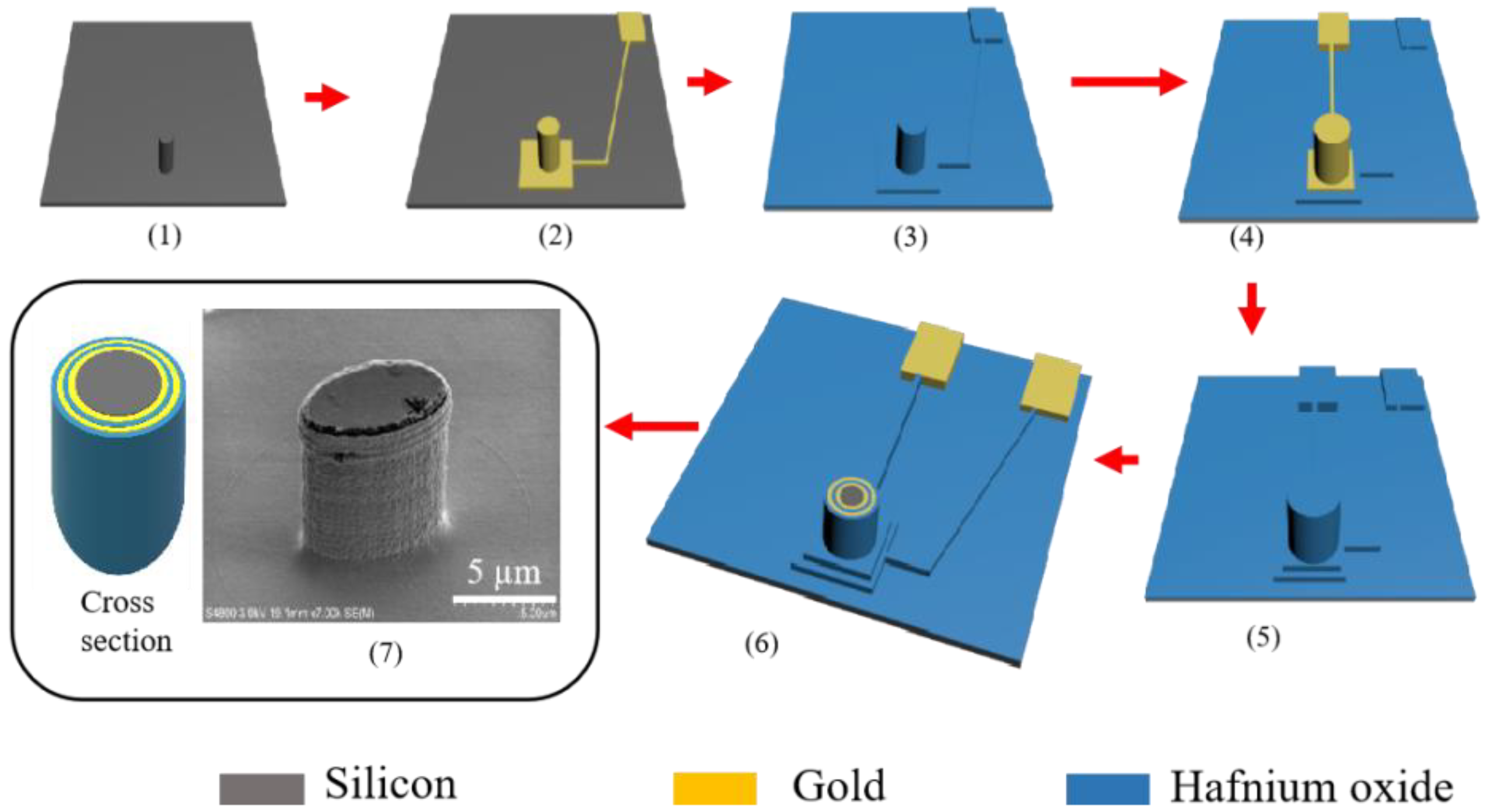
2.1. Microfabrication Processing
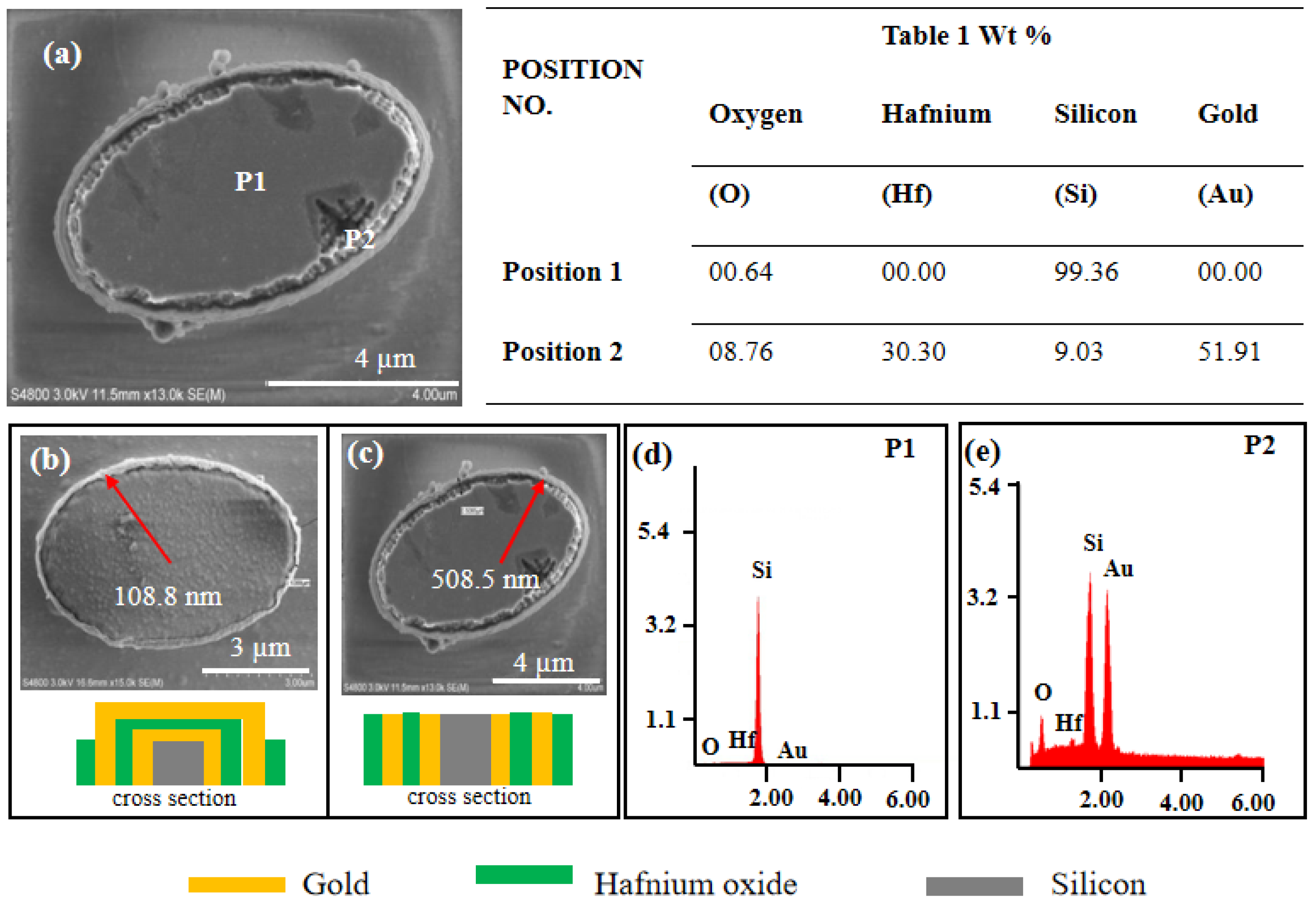
2.2. Morphology
2.3. Electrochemical Characterization
3. Results and Discussion
3.1. Surface Characterization of Si Micropillar and Au NREs
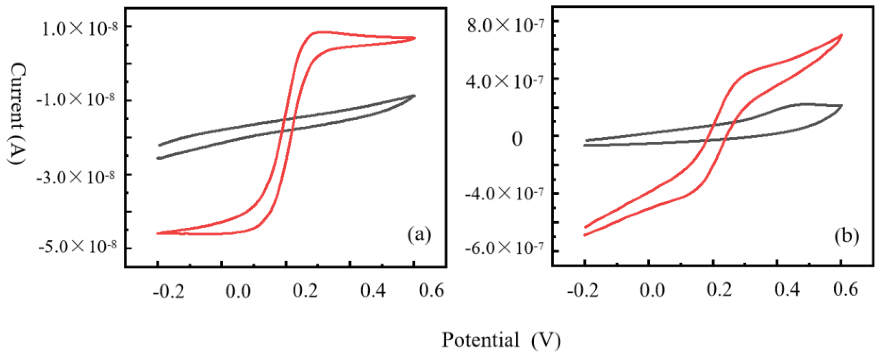
3.2. CV Theory and Analysis
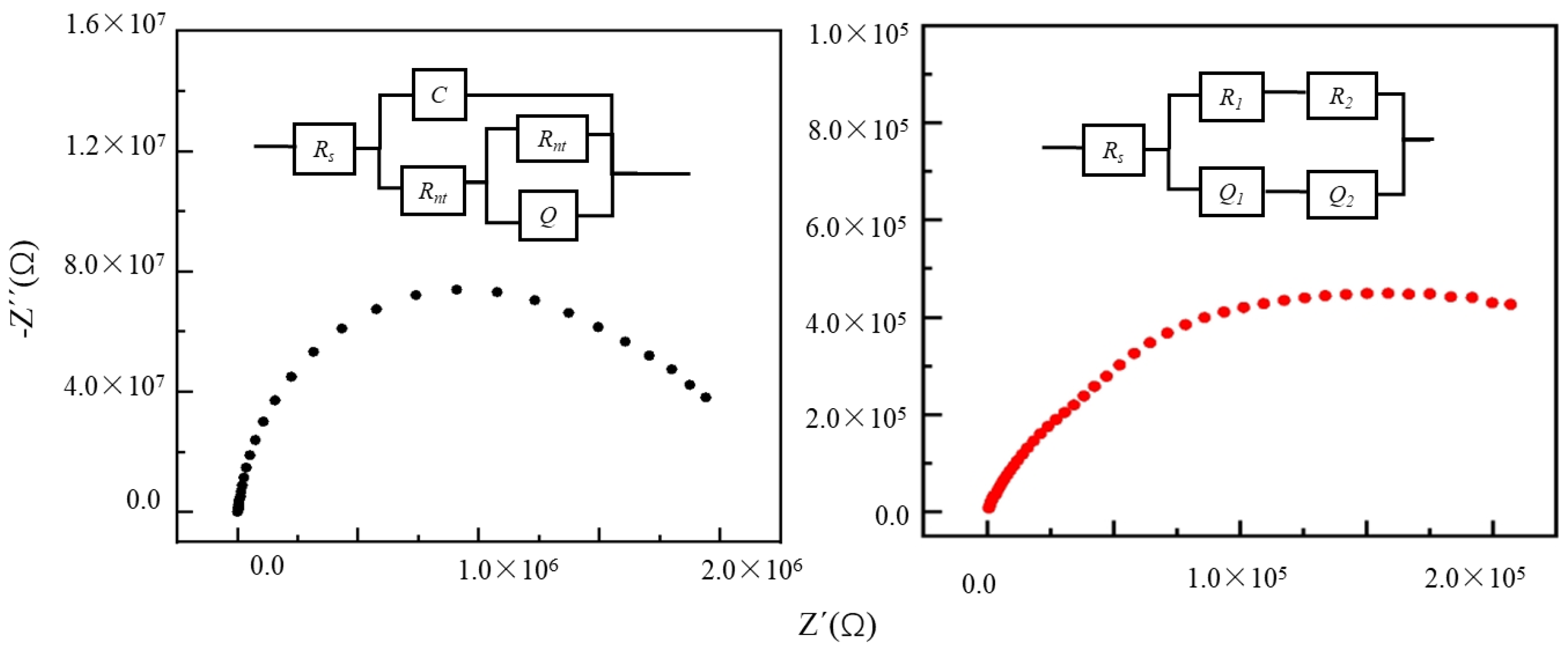
3.3. EIS Analysis
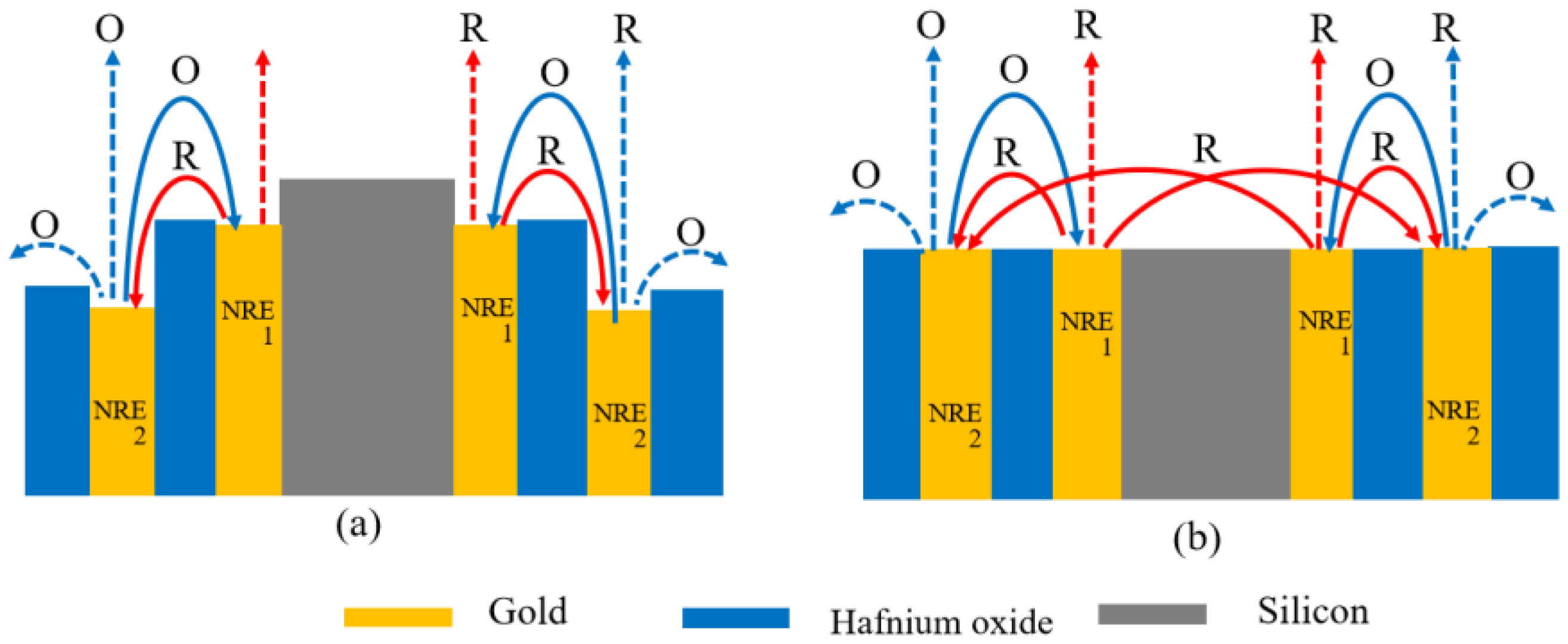
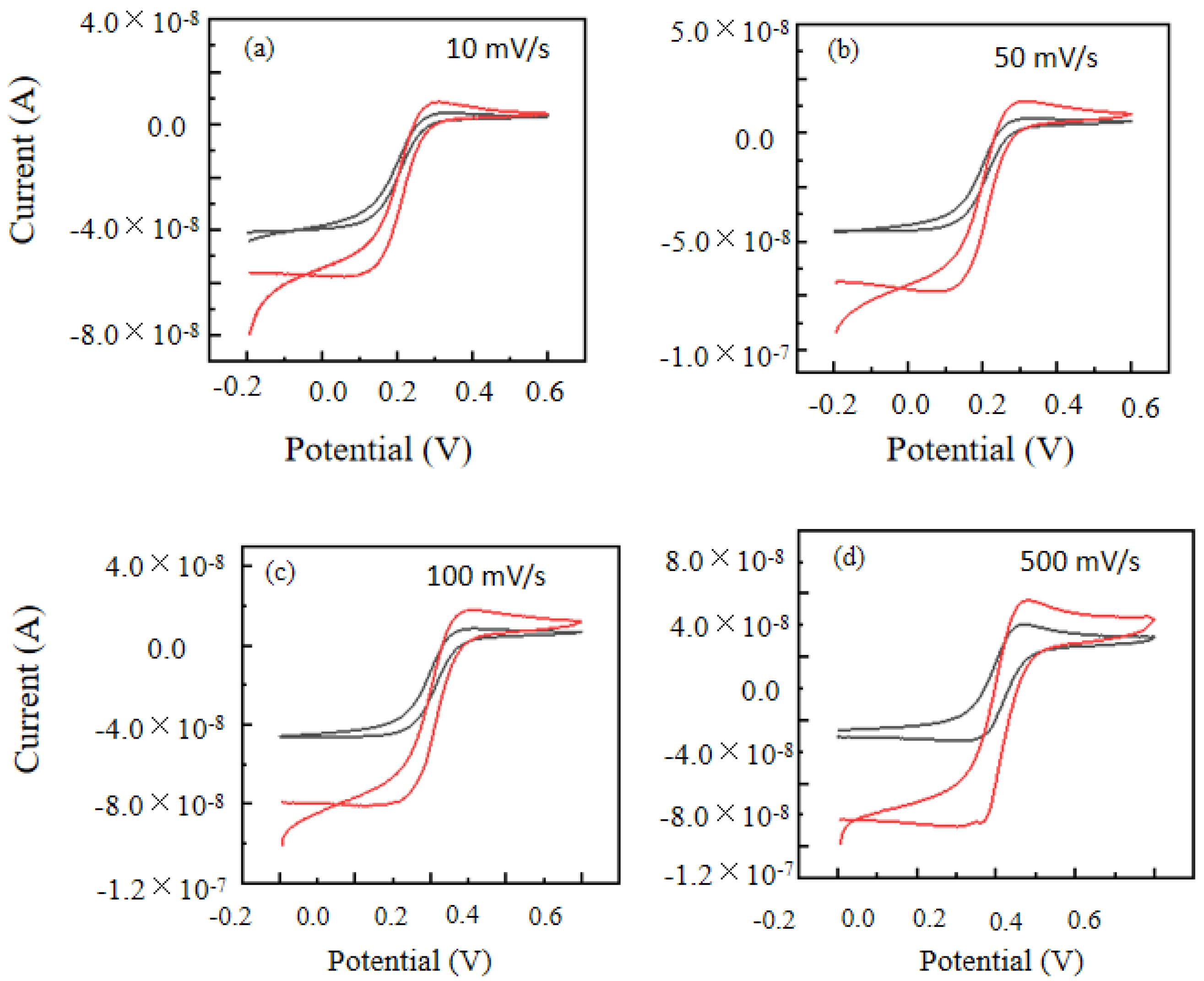
3.4. Redox Cycling
4. Conclusions
Author Contributions
Funding
Data Availability Statement
Acknowledgments
Conflicts of Interest
References
- Arrigian, D.W.M. Nanoelectrodes, nanoelectrode arrays and their applications. Analyst 2004, 129, 1157–1165. [Google Scholar] [CrossRef] [PubMed]
- Hasan, R.; Luo, X.; Sun, J. Rolling Nanoelectrode Lithography. Micromachines 2020, 11, 656. [Google Scholar] [CrossRef] [PubMed]
- Lin, R.; Lim, T.M.; Tran, T. Enhancement of mass transfer coefficient towards carbon nanotube nanoelectrode array. Sens. Actuators B Chem. 2018, 260, 1052–1058. [Google Scholar] [CrossRef]
- Al-Jeda, M.; Mena-Morcillo, E.; Chen, A. Micro-Sized pH Sensors Based on Scanning Electrochemical Probe Microscopy. Micromachines 2022, 12, 2143. [Google Scholar] [CrossRef] [PubMed]
- Anderson, S.; Bau, H.H. Carbon nanoelectrodes for single cell probing. Nanotechnology 2015, 26, 185101. [Google Scholar] [CrossRef] [Green Version]
- Compton, R.G.; Wildgoose, G.G.; Rees, N.V.; Streeter, I.; Baron, R. Design, fabrication, characterization, and application of nanoelectrode arrays. Chem. Phys. Lett. 2008, 459, 1–17. [Google Scholar] [CrossRef]
- Scholvin, J.; Zorzos, A.N.; Kinney, J.; Bernstein, J.G.; Boyden, E.S. Scalable, Modular Three-Dimensional Silicon Microelectrode Assembly via Electroless Plating. Micromachines 2018, 9, 436. [Google Scholar] [CrossRef] [Green Version]
- Watkins, J.J.; Chen, J.; White, H.S.; Abruña, H.D. Zeptomole voltammetric detection and electron-transfer rate measurements using platinum electrodes of nanometer dimensions. Anal. Chem. 2003, 75, 3962–3971. [Google Scholar] [CrossRef]
- Dayton, M.A.; Brown, J.C.; Stutts, K.J.; Wightman, R.M. Faradaic electrochemistry at microvoltammetric electrodes. Anal. Chem. 1980, 52, 946–950. [Google Scholar] [CrossRef]
- Triroj, N.; Jaroenapibal, P.; Shi, H.; Yeh, J.I.; Beresford, R. Microfluidic chip-based nanoelectrode array as miniaturized biochemical sensing platform for prostate-specific antigen detection. Biosens. Bioelectron. 2011, 26, 2927–2933. [Google Scholar] [CrossRef]
- Shi, H.; Yeh, J.I. Nanoelectrodes for Biomedical Applications. In Handbook of Nanobiomedical Research: Fundamentals, Applications and Recent Developments, Applications in Diagnostics, 1st ed.; World Scientific: Singapore, 2014. [Google Scholar] [CrossRef]
- Zhang, Y.; Lin, L.; Feng, Z.; Zhou, J. Fabrication of a PANI/Au nanocomposite modified nanoelectrode for sensitive dopamine nanosensor design. Electrochim. Acta 2010, 55, 265–270. [Google Scholar] [CrossRef]
- Zanut, A.; Cian, A.; Cefarin, N.; Pozzato, A.; Tormen, M. Nanoelectrode Arrays Fabricated by Thermal Nanoimprint Lithography for Biosensing Application. Biosensors 2020, 10, 90. [Google Scholar] [CrossRef]
- Moazzenzade, T.; Walstra, T.; Yang, X.; Huskens, J.; Lemay, S.G. Ring Ultramicroelectrodes for Current-Blockade Particle-Impact Electrochemistry. Anal. Chem. 2022, 94, 10168–10174. [Google Scholar] [CrossRef] [PubMed]
- Ma, C.; Contento, N.M.; Bohn, P.W. Redox cycling on recessed ring-disk nanoelectrode arrays in the absence of supporting electrolyte. J. Am. Chem. Soc. 2014, 136, 7225–7228. [Google Scholar] [CrossRef] [PubMed]
- Ma, C.; Contento, N.M.; Gibson, L.R., 2nd; Bohn, P.W. Recessed ring-disk nanoelectrode arrays integrated in nanofluidic structures for selective electrochemical detection. Anal. Chem. 2013, 85, 9882–9888. [Google Scholar] [CrossRef] [PubMed]
- Wang, D.; Dongmei, H.; Tang, H.; Yang, C.; Chen, W.; Li, Y. A signal amplification strategy and sensing application using single gold nanoelectrodes. Analyst 2018, 144, 310–316. [Google Scholar] [CrossRef] [PubMed]
- Gerhardt, I.; Wrigge, G.; Sandoghdar, V. Control and imaging of single-molecule spectral dynamics using a nano-electrode. Mol. Physics 2009, 107, 1975–1979. [Google Scholar] [CrossRef]
- Tang, H.; Zhu, J.; Xiao, X.; Wang, Z.; Wang, H.; Li, Y. Single mercury nanoelectrode: Single nucleus growth on Au nanoelectrode and its sensing application. Sens. Actuators B Chem. 2019, 282, 523–528. [Google Scholar] [CrossRef]
- Ma, C.; Contento, N.M.; Gibson, L.R.; Bohn, P.W. Redox Cycling in Nanoscale-Recessed Ring-Disk Electrode Arrays for Enhanced Electrochemical Sensitivity. ACS Nano 2013, 6, 5483–5490. [Google Scholar] [CrossRef]
- Ito, K.; Inoue, K.Y.; Ino, K.; Matsue, T.; Shiku, H. A highly sensitive endotoxin sensor based on redox cycling in a nanocavity. Analyst 2019, 144, 3659–3667. [Google Scholar] [CrossRef]
- Bartelt, J.E.; Deakin, M.R.; Amatore, C.; Wightman, R.M. Construction, and use of paired and triple band microelectrodes in solutions of low ionic strength. Anal. Chem. 1988, 60, 2167–2169. [Google Scholar] [CrossRef]
- Paixao, T.R.L.C.; Richter, E.M.; Brito-Neto, J.G.A.; Bertotti, M. Fabrication of a new generator-collector electrochemical microdevice: Characterization and applications. Electrochem. Commun. 2006, 8, 9–14. [Google Scholar] [CrossRef]
- Neugebauer, S.; Mueller, U.; Lohmueller, T.; Spatz, J.P.; Stelzle, M.; Schuhmann, W. Characterization of nanopore electrode structures as basis for amplified electrochemical assays. Electroanalysis 2006, 18, 1929–1936. [Google Scholar] [CrossRef]
- Menshykau, D.; del Campo, F.J.; Munoz, F.X.; Compton, R.G. Current collection efficiency of micro- and nanoring-recessed disk electrodes and of arrays of these electrodes. Sens. Actuators B Chem. 2009, 138, 362–367. [Google Scholar] [CrossRef]
- Luo, L.; White, H.S. Electrogeneration of Single Nanobubbles at Sub-50-nm-Radius Platinum Nanodisk Electrodes. Langmuir 2013, 35, 11169–11175. [Google Scholar] [CrossRef] [PubMed]
- Guerrette, J.P.; Percival, S.J.; Zhang, B. Voltammetric behavior of gold nanotrench electrodes. Langmuir 2011, 27, 12218. [Google Scholar] [CrossRef]
- Schmueser, I.; Walton, A.J.; Terry, J.G.; Woodvine, H.L.; Freeman, N.J.; Mount, A.R. A systematic study of the influence of nanoelectrode dimensions on electrode performance and the implications for electroanalysis and sensing. Faraday Discuss 2013, 164, 295–314. [Google Scholar] [CrossRef] [PubMed] [Green Version]
- Guerrette, J.P.; Oja, S.M.; Zhang, B. Coupled electrochemical reactions at bipolar microelectrodes and nanoelectrodes. Anal. Chem. 2012, 84, 1609–1616. [Google Scholar] [CrossRef] [PubMed]
- Chen, C.; Teng, W.; Hahn, J.H. Nanoband electrode for high-performance in-channel amperometric detection in dualchannel microchip capillary electrophoresis. Electrophoresis 2011, 32, 838–843. [Google Scholar] [CrossRef]
- Falk, M.; Sultana, R.; Swann, M.J.; Mount, A.R.; Freeman, N.J. Nanoband array electrode as a platform for high sensitivity enzyme-based glucose biosensing bioelechem. Bioelectrochemistry 2016, 112, 100–105. [Google Scholar] [CrossRef] [PubMed] [Green Version]
- Arnold, M.; Cavalcanti-Adam, E.A.; Class, R.; Blümmel, J.; Eck, W.; Kantlehner, M.; Kessler, H.; Spatz, J.P. Activation of integrin function by nanopatterned adhesive interfaces, Chem. Phys. Chem. 2004, 19, 383–388. [Google Scholar] [CrossRef]
- Roos, W.; Ulmer, J.; Gräter, S.; Surrey, T.; Spatz, J.P. Microtubule gliding and crosslinked microtubule networks on micropillar interfaces. Nano Lett. 2005, 5, 2630–2634. [Google Scholar] [CrossRef]
- Kim, W.; Ng, J.K.; Kunitake, M.E.; Conklin, B.R.; Yang, P. Interfacing silicon nanowires with mammalian cell. J. Am. Chem. Soc. 2007, 129, 7228–7229. [Google Scholar] [CrossRef] [PubMed]
- Xie, C.; Hanson, L.; Xie, W.; Lin, Z.; Cui, B.; Cui, Y. Noninvasive neuron pinning with nanopillar arrays. Nano Lett. 2010, 10, 4020–4024. [Google Scholar] [CrossRef] [PubMed] [Green Version]
- Yin, H.; Tan, C.; Siddiqui, S.; Arumugam, P. Electrochemical behavior of a gold nanoring electrode microfabricated on a silicon micropillar. Sens. Actuators B Chem. 2004, 281, 392–398. [Google Scholar] [CrossRef]
- Dixit, P.; Miao, J. Effect of SF6 flow rate on the etched surface profile and bottom grass formation in deep reactive ion etching process. J. Phys. Conf. Ser. 2006, 34, 577–582. [Google Scholar] [CrossRef]
- Cheung, C.L.; Nikolić, R.J.; Reinhardt, C.E.; Wang, T.F. Fabrication of nanopillars by nanosphere lithography. Nanotechnology 2006, 17, 1339–1343. [Google Scholar] [CrossRef]
- Frommhold, A.; Robinson, A.P.G.; Tarte, E. High aspect ratio silicon and polyimide nanopillars by combination of nanosphere lithography and intermediate mask pattern transfer. Microelectron. Eng. 2012, 99, 43–49. [Google Scholar] [CrossRef]
- Robertson, J. High dielectric constant oxides. Eur. Phys. J. Appl. Phys. 2004, 28, 265–291. [Google Scholar] [CrossRef] [Green Version]
- Hausmann, D.M.; Gordon, R.G. Surface morphology and crystallinity control in the atomic layer deposition (ALD) of hafnium and zirconium oxide thin films. J. Cryst. Growth 2003, 249, 251–261. [Google Scholar] [CrossRef]
- Lee, J.H.; Kim, J.P.; Lee, J.T.; Kim, Y.S.; Jung, H.S.; Lee, N.I.; Kang, H.K.; Suh, K.P.; Jeong, M.M.; Hyun, K.T.; et al. Mass production worthy HfO2-Al2O3 laminate capacitor technology using Hf liquid precursor for sub-100nm DRAMs. In Proceedings of theDigest. International Electron Devices Meeting, San Francisco, CA, USA, 8–11 December 2002; pp. 221–224. [Google Scholar] [CrossRef]
- Bard, A.J.; Faulkner, L.R. Electrochemical Methods, 2nd ed.; John Wiley & Sons: New York, NY, USA, 2001; p. 833. [Google Scholar]
- Lanyon, Y.H.; Arrigan, D.W.M. Recessed nanoband electrodes fabricated by focused ion beam milling. Sens. Actuators B 2007, 121, 341–347. [Google Scholar] [CrossRef]
- Lantiat, D.; Vivier, V.; Laberty-Robert, C.; Grosso, D.; Sanchez, C. Gold nanoelectrode arrays and their evaluation by impedance spectroscopy and cyclic voltammetry. Chem. Phys. Chem. 2010, 11, 1971–1977. [Google Scholar] [CrossRef]
- Hees, J.; Hoffmann, R.; Kriele, A.; Smirnov, W.; Obloh, H.; Glorer, K.; Raynor, B.; Driad, R.; Yang, N.; Williams, O.A.; et al. Nanocrystalline diamond nanoelectrode arrays and ensembles. ACS Nano 2011, 5, 3339–3346. [Google Scholar] [CrossRef] [PubMed]
- Gholizadeh, A.; Shahrokhian, S.; Irajizad, A.; Mohajerzadeh, S.; Vosoughi, M.; Darbari, S.; Koohsorkhi, J.; Mehran, M. Fabrication of sensitive glutamate biosensor based on vertically aligned CNT nanoelectrode array and investigating the effect of CNTs density on the electrode performance. Anal. Chem. 2012, 84, 5932–5938. [Google Scholar] [CrossRef]
- Siddiqui, S.; Arumugam, P.U.; Chen, H.; Li, J.; Meyyappan, M. Characterization of carbon nanofiber electrode arrays using electrochemical impedance spectroscopy: Effect of scaling down electrode size. ACS Nano 2010, 4, 955–961. [Google Scholar] [CrossRef]
- Steil, M.C.; Thevenot, F.; Kleitz, M. Densification of Yttria-stabilized zirconia impedance spectroscopy analysis. J. Electrochem. Soc. 1997, 144, 390–398. [Google Scholar] [CrossRef]
- De Florio, D.Z.; Muccillo, R. Sintering of zirconia-yttria ceramics studied by impedance spectroscopy. Solid State Ion. 1999, 123, 301–305. [Google Scholar] [CrossRef]
- Amirudin, A.; Thieny, D. Application of electrochemical impedance spectroscopy to study the degradation of polymer-coated metals. Prog. Org. Coat. 1995, 26, 1–28. [Google Scholar] [CrossRef]
- Bruce, P.G.; Lisowska-Oleksiak, A.; Los, P.; Vincent, C.A. Electrochemcial impedance spectroscopy at an ultramicroelectrode. J. Electroanal. Chem. 1994, 367, 279–283. [Google Scholar] [CrossRef]
- Kang, J.; Ko, Y.; Park, J.; Kim, D. Origin of Capacity Fading in Nano-Sized Co3O4 Electrodes: Electrochemical Impedance Spectroscopy Study. Nanoscale Res. Lett. 2008, 3, 390–394. [Google Scholar] [CrossRef] [Green Version]
- Inaba, A.; Takei, Y.; Kan, T.; Matsumoto, K.; Shimoyama, I. Electrochemical impedance measurement of a carbon nanotube probe electrode. Nanotechnology 2012, 23, 485302. [Google Scholar] [CrossRef] [PubMed]
- Huang, W.; McCreery, R. Electron transfer kinetics of Fe(CN)3-/4- on laser-activated and CN-modified Pt electrodes. J. Electroanal. Chem. 1992, 326, 1–12. [Google Scholar] [CrossRef]


| Scan Rate | Non-RC Mode (nA) | RC Mode (nA) | Amplification |
|---|---|---|---|
| 10 mV/s | 29.3 | 47.5 | 1.63 |
| 50 mV/s | 43.7 | 59.3 | 1.36 |
| 100 mV/s | 48.9 | 65.2 | 1.34 |
| 500 mV/s | 64.9 | 86.6 | 1.30 |
| Scan Rate | i2,a (nA) | i1,c (nA) | Φ2 |
|---|---|---|---|
| 10 mV/s | 42.3 | 46.5 | 90.7% |
| 50 mV/s | 40.6 | 61.8 | 65.7% |
| 100 mV/s | 42.7 | 70.5 | 60.6% |
| 500 mV/s | 47.1 | 110.5 | 40.2% |
Disclaimer/Publisher’s Note: The statements, opinions and data contained in all publications are solely those of the individual author(s) and contributor(s) and not of MDPI and/or the editor(s). MDPI and/or the editor(s) disclaim responsibility for any injury to people or property resulting from any ideas, methods, instructions or products referred to in the content. |
© 2023 by the authors. Licensee MDPI, Basel, Switzerland. This article is an open access article distributed under the terms and conditions of the Creative Commons Attribution (CC BY) license (https://creativecommons.org/licenses/by/4.0/).
Share and Cite
Yin, H.; Tan, C.; Siddiqui, S.; Arumugam, P.U. Electrochemical Redox Cycling Behavior of Gold Nanoring Electrodes Microfabricated on a Silicon Micropillar. Micromachines 2023, 14, 726. https://doi.org/10.3390/mi14040726
Yin H, Tan C, Siddiqui S, Arumugam PU. Electrochemical Redox Cycling Behavior of Gold Nanoring Electrodes Microfabricated on a Silicon Micropillar. Micromachines. 2023; 14(4):726. https://doi.org/10.3390/mi14040726
Chicago/Turabian StyleYin, Haocheng, Chao Tan, Shabnam Siddiqui, and Prabhu U. Arumugam. 2023. "Electrochemical Redox Cycling Behavior of Gold Nanoring Electrodes Microfabricated on a Silicon Micropillar" Micromachines 14, no. 4: 726. https://doi.org/10.3390/mi14040726