Communication

Analytical and Physical Investigation on Source Resistance in InxGa1−xAs Quantum-Well High-Electron-Mobility Transistors

1
School of Electronic and Electrical Engineering, Kyungpook National University (KNU), Daegu 41566, Republic of Korea
2
NTT Device Technology Laboratories, Atsugi-shi 243-0198, Japan
*
Author to whom correspondence should be addressed.
Micromachines 2023, 14(2), 439; https://doi.org/10.3390/mi14020439
Submission received: 15 January 2023 / Revised: 27 January 2023 / Accepted: 8 February 2023 / Published: 12 February 2023
(This article belongs to the Special Issue Feature Papers of Micromachines in Engineering and Technology 2022)

Abstract

:
We present a fully analytical model and physical investigation on the source resistance (RS) in InxGa1−xAs quantum-well high-electron mobility transistors based on a three-layer TLM system. The RS model in this work was derived by solving the coupled quadratic differential equations for each current component with appropriate boundary conditions, requiring only six physical and geometrical parameters, including ohmic contact resistivity (ρc), barrier tunneling resistivity (ρbarrier), sheet resistances of the cap and channel regions (Rsh_cap and Rsh_ch), side-recessed length (Lside) and gate-to-source length (Lgs). To extract each model parameter, we fabricated two different TLM structures, such as cap-TLM and recessed-TLM. The developed RS model in this work was in excellent agreement with the RS values measured from the two TLM devices and previously reported short-Lg HEMT devices. The findings in this work revealed that barrier tunneling resistivity already played a critical role in reducing the value of RS in state-of-the-art HEMTs. Unless the barrier tunneling resistivity is reduced considerably, innovative engineering on the ohmic contact characteristics and gate-to-source spacing would only marginally improve the device performance.

1. Introduction

The evolving sixth-generation (6G) wireless communication technologies demand higher operating frequencies of approximately 300 GHz with data rates approaching 0.1 Tbps [1,2]. To meet this urgent requirement, transistor technologies must be engineered to sustain the evolution of digital communication systems, guided by Edholm’s law [3]. Among various transistor technologies, indium-rich InxGa1−xAs quantum-well (QW) high-electron-mobility transistors (HEMTs) on InP substrates have offered the best balance of current-gain cutoff frequency (fT) and maximum oscillation frequency (fmax), and the lowest noise figure characteristics in the sub-millimeter-wave region [4,5,6,7,8]. These transistors adopt a combination of Lg scaling down to sub-30 nm, enhancement of the channel carrier transport by incorporating the indium-rich channel design, and reduction of all parasitic components.
Among various parasitic components, it is imperative to minimize the source resistance (RS) itself to fully benefit from the superior intrinsic performance of the InxGa1−xAs QW channel [9,10], demanding an analytical and physical model for the source resistance. Considering state-of-the-art InxGa1−xAs HEMT technologies [11,12,13,14], source and drain contacts have been created with a non-alloyed metal stack of Ti/Pt/Au with a source-to-drain spacing (Lds) between 1 μm and 0.5 μm. Historically, RS is minimized by reducing the ohmic contact resistivity (ρc) [15] and shrinking the gate-to-source spacing (Lgs) using da self-aligned gate architecture [16,17]. However, it is very challenging to reduce RS to below 100 Ω·μm, because of the tunneling resistance component between the heavily doped In0.53Ga0.47As capping layer and the InxGa1−xAs QW channel layer. To understand the limit of RS in HEMTs in an effort to further reduce RS, a sophisticated and comprehensive model must be developed for RS in state-of-the art HEMTs, rather than the simple lumped-elements-based one-layer model [18,19].
Previously, two-layer system-based RS model was developed by Feuer [20], which was applicable to alloyed ohmic contact structures with two different contact resistances: one was associated with a heavily doped GaAs capping layer and the other with a undoped GaAs QW channel layer. In this letter, we present a fully analytical and physical model for RS in advanced HEMTs, requiring only six physical and geometrical parameters. The model considers three different regions: (i) a one-layer transmission-line model (TLM) for the side-recess region, (ii) an analytical TLM for the access region and (iii) an analytical three-layer TLM for the source electrode region, to accurately predict a value of RS in a given HEMT structure and identify dominant components to further minimize RS. To do so, we proposed and fabricated two different types of TLM structures to experimentally extract each component of RS. The analytical model proposed in this work is in excellent agreement with the measured values of RS from the fabricated r-TLMs, as well as recently reported advanced HEMTs. Most importantly, findings in this work reveal that the ρbarrier is a bottleneck for further reductions of RS in advanced HEMTs.

2. Analytical Model for RS

Figure 1a–c show the cross-sectional schematic and TEM images of advanced InxGa1−xAs QW HEMTs on an InP substrate [4]. They adopt non-alloyed S/D ohmic contacts such as a metal stack of Ti/Pt/Au with contact resistance (RC) values between 10 Ω·μm and 20 Ω·μm. Carrier transfer from the cap to channel replies on a tunneling mechanism via an In0.52Al0.48As barrier layer. To model RS, a comprehensive transport mechanism from the source ohmic electrode to the InxGa1−xAs QW channel via the In0.53Ga0.47As cap and In0.52Al0.48As barrier layers must be considered in a distributed manner.
Figure 2a illustrates a complete distributed equivalent circuit model for RS, comprising three regions. One is the source ohmic electrode region (Region-I), where the electrons are injected from the ohmic metal to the In0.53Ga0.47As cap and then to the InxGa1−xAs QW channel through the In0.52Al0.48As barrier, which is governed by a three-layer TLM system. Another is the source access region (Region-II), where the electron transfer mechanism is governed by a cap-to-channel two-layer TLM system with transfer length (LT_barrier) given by ρ b a r r i e r / ( R s h _ c h + R s h _ c a p ) . The other is the side-recessed region (Region-III), where a simple one-layer model works. In comparison, lumped-elements based one-layer model is shown in Figure 2c [18,19].
Next, let us derive a fully analytical and physical expression for RS. Given the coordinate system in Figure 3a, RS can be determined by Vch(x = −Lgs)/IO from Ohm’s law, and then the problem is how to express each current component as a function of x such as Ich(x), Icap(x), and Imet(x). In a given segment as highlighted in Figure 3b, we can define a differential contact conductance as dgc = (Wg/ρc) dx, a differential barrier conductance as dgbarrier = (Wg/ρbarrier) dx, a differential lateral cap resistance as drs_cap = (Rsh_cap/Wg) dx and a differential lateral channel resistance as drs_ch = (Rsh_ch/Wg) dx. At location x, Kirchhoff’s current and voltage laws yield, respectively
d 2 I m e t ( x ) d x 2 = [ R m e t · I m e t ( x ) R s h _ c h · I c a p ( x ) ] ρ c 1
d 2 I c h ( x ) d x 2 = [ R s h _ c h · I c h ( x ) R s h _ c a p · I c a p ( x ) ] ρ b a r r i e r 1
I c a p = I O I m e t I c h
These are coupled quadratic differential equations for three current components (Ich(x), Icap(x) and Imet(x)). From the general solution for these differential equations with existing six boundary conditions (listed in Table 1), we obtain an analytical expression for Ich(x), Icap(x), and Imet(x) for both regions, as written in Table 1. The expression for Vch(x = −Lgs) can then be derived. Although there are several ways to express Vch(x = −Lgs), it is useful to focus on the total voltage drop across the InxGa1−xAs QW channel from x = −Lgs to x = ∞ in this work. From this,
V c h ( x = L g s ) = I c h ( x ) · d r S _ c h   d x
The source resistance, defined as Vch(x = 0)/IO, is
R S = V c h ( x = L g s ) I O = R s h _ c h W g I O L g s I c h ( x ) d x
R S · W g = [ 2 · C 1 · ρ C · ρ b a r r i e r ρ C · ( R s h _ c h + R s h _ c a p ) + ρ b a r r i e r · R s h _ c a p η + 2 · C 1 · ρ C · ρ b a r r i e r ρ C · ( R s h _ c h + R s h _ c a p ) + ρ b a r r i e r · R s h _ c a p + η + ( C 3 C 4 ) · ( 1 e L g s / L T _ b a r r i e r ) L T _ b a r r i e r + R s h _ c a p · L g s ρ b a r r i e r · L T _ b a r r i e r 2 ] + R s h _ c h · L s i d e
η = ρ c 2 ( R s h _ c h 2 + R s h _ c a p 2 ) + 2 R s h _ c h   R s h _ c a p ρ c ( ρ c ρ b a r r i e r ) + R s h _ c a p 2 ρ b a r r i e r ( 2 ρ c + ρ b a r r i e r )
L T _ b a r r i e r = ρ b a r r i e r R s h _ c h + R s h _ c a p
Overall, RS depends on the ohmic contact resistivity, the sheet resistances of the cap and QW channel layers, the barrier tunneling resistivity, and the length of the gate-to-source region and side-recessed regions.

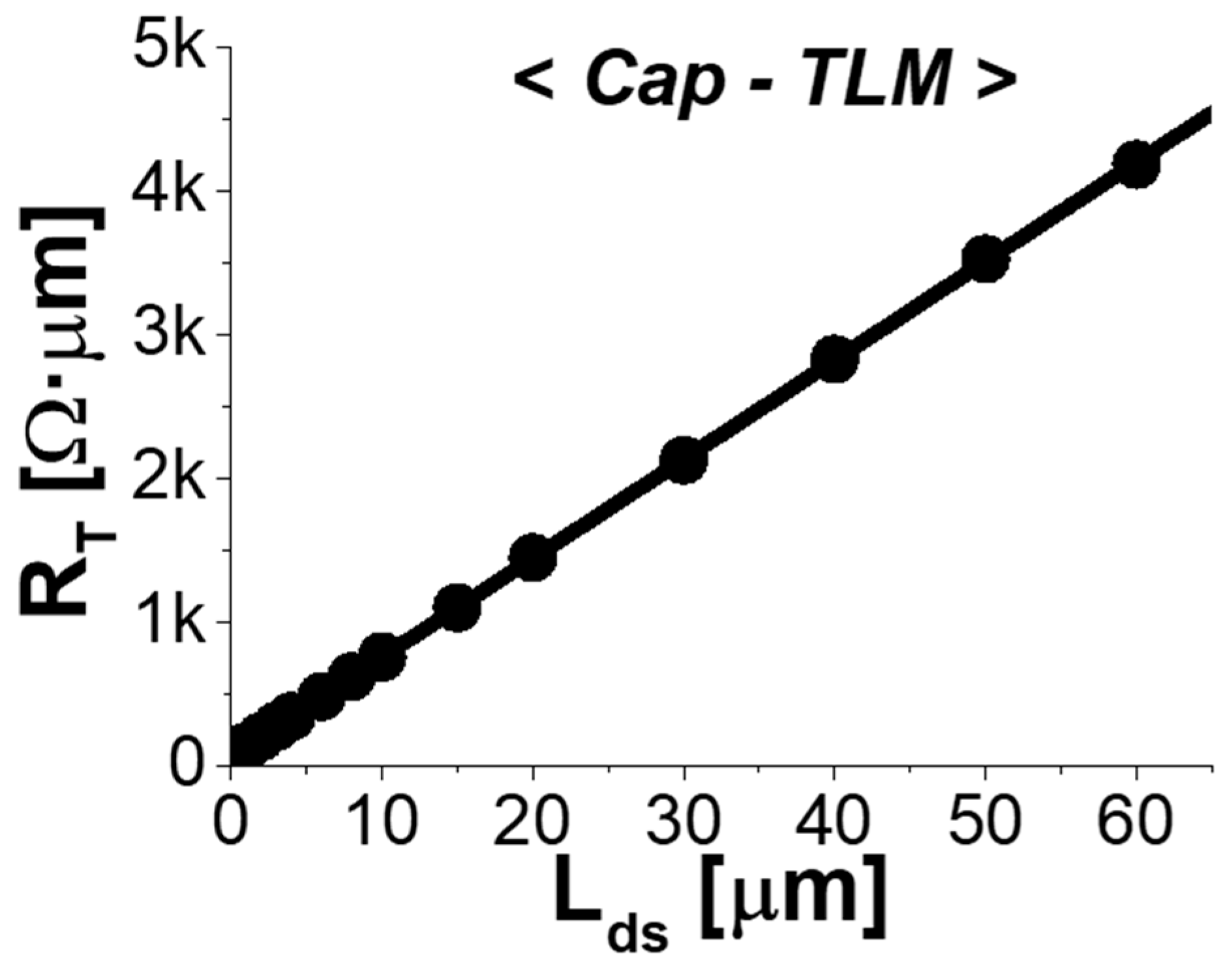
3. Experimental Results and Discussion

Two types of TLM structures were fabricated, as shown in Figure 3: the cap-only TLM structure (cap-TLM, (a)) to evaluate the contact characteristics of the non-alloyed ohmic metal stack, and the recessed TLM structure (r-TLM, (b)) which is identical to the real device without a Schottky gate electrode. Details on the epitaxial layer design and device processing were reported in our previous paper [4]. All device processing was conducted on a full 3-inch wafer with an i-line stepper to ensure fine alignment accuracy within 0.05 μm. In the r-TLM, we varied Lg from 40 μm to 0.5 μm and Lgs from 10 μm to 0.2 μm. In this way, the split of Lg yielded the sheet resistance of the QW channel (Rsh_ch) from the linear dependence, and the source resistance (RS) from the y-intercept at a given Lgs. Lastly, we investigated the dependence of RS on Lgs in detail.
Figure 4 plots the measured total resistance (RT) against Lds, which corresponds to the length between the edge of source and the edge of drain. for the fabricated cap-TLM structures. This yielded values of Rsh_cap = 131 Ω/sq, RC = 32 Ω·μm, LT_cap = 0.34 μm and ρc = 15 Ω·μm2, with an excellent correlation coefficient of 0.99999. Figure 5a plots the measured RT against Lg for the r-TLM structures with various dimensions of Lgs from 10 μm to 0.2 μm. When Lg was long enough, each r-TLM device yielded approximately the same slope for all Lgs with excellent correlation coefficient. This is plotted in Figure 5b with averaged Rsh_ch = 145 Ω/sq and excellent ∆(Rsh_ch) = 1.56 Ω/sq, confirming that the In0.8Ga0.2As QW channel sheet resistance was independent of Lgs. Because we designed the symmetrical Lgs and Lgd, half of the y-intercept from Figure 6a corresponded exactly to RS. In analyzing r-TLM structures with various Lgs, values of the correlation coefficient were also greater than 0.999, increasing the credibility of the overall TLM analysis.
Figure 6 plots the measured RS (filled symbols) from the r-TLM analysis against Lgs, as well as the projected RS (line) from Equation (5) with the model parameters of ρbarrier = 91 Ω·μm2 and others directly from the cap-TLMs and r-TLMs. Additionally, the open symbols in Figure 6 came from the RS extracted directly from the reported HEMTs [4] using the gate-current injection technique [21]. There are two points to identify in Figure 6. First, all of the measured RS characteristics were explained by the modeled RS. Second, RS was linearly proportional to Lgs for Lgs > 1 μm, where its slope was 69 Ω/sq. Interestingly, this was similar to the parallel connection of Rsh_cap and Rsh_ch. However, this linear dependence of RS on Lgs was no longer valid for Lgs < 1 μm and, most importantly, the measured RS eventually saturated to approximately 123 Ω·μm even with Lgs approaching 0. Our model clearly indicated that this was because of the barrier tunneling resistivity. The saturation of RS in Lgs = 0 was because the necessary lateral length for the cap-to-channel tunneling was supplied by its equivalent transfer length from the leading edge of the source metal contact (−LT_barrier < x < 0) in Region-I.
Finally, let us discuss how to further reduce RS with the RS model proposed in this work. The three solid lines in Figure 6 are the model projections of RS with the ohmic contact resistivity improve from 15 Ω·μm2 (present) to 1 Ω·μm2. Surprisingly, RS would not be minimized even with a significant reduction in ρc and Lgs because of the ρbarrier. Alternatively, the three dashed lines in Figure 6 are from the same model projection, but with ρbarrier = 20 Ω·μm2. Note that a reduction in the ρbarrier is important; in consequence, the projected RS would be significantly scaled down to 70 Ω·μm and below. Under this circumstance, RS could then be further reduced by the improved ohmic contact characteristics and the reduction of Lgs.

4. Conclusions

A fully analytical and physical investigation on RS in advanced InxGa1−xAs QW HEMTs was carried out with a three-layer TLM system. Analytical solutions to the three current components (source metal, cap, and channel) along the selected coordinate system with appropriate boundary conditions were produced. The proposed RS model in this work required only six physical and geometrical parameters (ρc, ρbarrier, Rsh_cap, Rsh_ch, Lside and Lgs), yielding excellent agreement with the RS values measured from the two TLM devices and previously reported InxGa1−xAs QW HEMTs. The developed model in this work was capable of explaining the saturation behavior of RS for Lgs < 1 μm, which was due to the ρbarrier. Therefore, one must pay a more careful attention to cut down the ρbarrier to further minimize RS in future HEMTs.

Author Contributions

Conceptualization, J.-H.Y. and D.-H.K.; device fabrication, J.-H.Y., I.-G.L. and D.-H.K.; formal analysis, J.-H.Y., T.T., H.S., H.M. and D.-H.K.; investigation, J.-H.Y., J.-H.L. and D.-H.K.; resources, J.-H.Y., J.-H.L. and D.-H.K.; writing—original draft preparation, J.-H.Y.; writing—review and editing, I.-G.L.; supervision, J.-H.L. and D.-H.K.; funding acquisition, D.-H.K. All authors have read and agreed to the published version of the manuscript.

Funding

This research was supported by the Civil-Military Technology Cooperation program (No. 19-CM-BD-05).

Data Availability Statement

The data presented in this study are available on request from the corresponding author.

Conflicts of Interest

The authors declare no conflict of interest.

References

  1. Cahoon, N.; Srinivasan, P.; Guarin, F. 6G Roadmap for Semiconductor Technologies: Challenges and Advances. In Proceedings of the IEEE International Reliability Physics Symposium, Dallas, TX, USA, 27–31 March 2022. [Google Scholar]
  2. Ikram, M.; Sultan, K.; Lateef, M.F.; Alqadami, A.S.M. A Road towards 6G Communication—A Review of 5G Antennas, Arrays, and Wearable Devices. Electronics 2022, 11, 169. [Google Scholar] [CrossRef]
  3. Cherry, S. Edholm’s law of bandwidth. IEEE Spectr. 2004, 41, 7. [Google Scholar] [CrossRef]
  4. Jo, H.-B.; Yun, S.-W.; Kim, J.G.; Yun, D.-Y.; Lee, I.G.; Kim, D.-H.; Kim, T.-W.; Kim, S.-K.; Yun, J.; Kim, T.; et al. Lg = 19 nm In0.8Ga0.2As composite channel HEMTs with fT = 738 GHz and fmax = 492 GHz. In Proceedings of the IEEE International Electron Devices Meeting, San Francisco, CA, USA, 12–18 December 2020. [Google Scholar]
  5. Cooke, C.M.; Leong, K.M.K.H.; Zamora, A.; Gorospe, B.S.; Mei, X.B.; Kangaslahti, P.; Schlecht, E.; Ogut, M.; Goncharenko, Y.; Reising, S.C.; et al. A 670 GHz Integrated InP HEMT Direct-Detection Receiver for the Tropospheric Water and Cloud Ice Instrument. IEEE Trans. Electron Devices 2021, 11, 566. [Google Scholar] [CrossRef]
  6. Leuther, A.; Koch, S.; Tessmann, A.; Kallfass, I.; Merkle, T.; Massler, H.; Loesch, R.; Schlechtweg, M.; Saito, S.; Ambacher, O. 20 NM metamorphic HEMT WITH 660 GHZ FT. In Proceedings of the International Conference on Indium Phosphide and Related Materials, Berlin/Heidelberg, Germany, 22–26 May 2011. [Google Scholar]
  7. Yun, S.-W.; Jo, H.-B.; Yoo, J.-H.; Park, W.-S.; Jeong, H.-S.; Choi, S.-M.; Kim, H.-J.; George, S.; Beak, J.-M.; Lee, I.-G.; et al. InxGa1−xAs quantum-well high-electron-mobility transistors with a record combination of fT and fmax: From the mobility relevant to ballistic transport regimes. In Proceedings of the IEEE Electron Devices Meeting, San Francisco, CA, USA, 11–16 December 2021. [Google Scholar]
  8. Takahashi, T.; Kawano, Y.; Makiyama, K.; Shiba, S.; Sato, M.; Nakasha, Y.; Hara, N. Enhancement of fmax to 910 GHz by Adopting Asymmetric Gate Recess and Double-Side-Doped Structure in 75-nm-Gate InAlAs/InGaAs HEMTs. IEEE Trans. Electron Devices 2017, 64, 89–95. [Google Scholar] [CrossRef]
  9. Tasker, P.J.; Hughes, B. Importance of source and drain resistance to the maximum f/sub T/ of millimeter-wave MODFETs. IEEE Electron. Device Lett. 1989, 10, 291–293. [Google Scholar] [CrossRef]
  10. Shinohara, K.; Yamashita, Y.; Endoh, A.; Watanabe, I.; Hikosaka, K.; Matsui, T.; Mimura, T.; Hiyamizu, S. 547-GHz f/sub t/ In/sub 0.7/Ga/sub 0.3/As-In/sub 0.52/Al/sub 0.48/As HEMTs with reduced source and drain resistance. IEEE Electron. Device Lett. 2004, 25, 241–243. [Google Scholar] [CrossRef]
  11. Chang, E.-Y.; Kuo, C.-I.; Hsu, H.-T.; Chiang, C.-Y.; Miyamoto, Y. InAs Thin-Channel High-Electron-Mobility Transistors with Very High Current-Gain Cutoff Frequency for Emerging Submillimeter-Wave Applications. Appl. Phys. Express 2013, 6, 034001. [Google Scholar] [CrossRef]
  12. Jo, H.-B.; Yun, S.-W.; Kim, J.-G.; Baek, J.-M.; Lee, I.-G.; Kim, D.-H.; Kim, T.-W.; Kim, S.-K.; Yun, J.; Kim, T.; et al. Sub-30-nm In0.8Ga0.2As Composite-Channel High-Electron-Mobility Transistors With Record High-Frequency Characteristics. IEEE Trans. Electron. Devices 2021, 68, 2010–2016. [Google Scholar] [CrossRef]
  13. Mei, X.; Yoshida, W.; Lange, M.; Lee, J.; Zhou, J.; Liu, P.-H.; Leong, K.; Zamora, A.; Padilla, J.; Sarkozy, S.; et al. First Demonstration of Amplification at 1 THz Using 25-nm InP High Electron Mobility Transistor Process. IEEE Electron. Device Lett. 2015, 36, 327–329. [Google Scholar] [CrossRef]
  14. Yun, D.-Y.; Jo, H.-B.; Son, S.-W.; Baek, J.-M.; Lee, J.-H.; Kim, T.-W.; Kim, D.-H.; Tsutsumi, T.; Sugiyama, H.; Matsuzaki, H. Lg=87 nm InAlAs/InGaAs High-Electron- Mobility Transistors With a g m_max of 3 S/mm and fT of 559 GHz. IEEE Electron. Device Lett. 2018, 39, 1640–1643. [Google Scholar]
  15. Crook, A.M.; Lind, E.; Griffith, A.; Rodwell, W.M.J. Low resistance, nonalloyed Ohmic contacts to InGaAs. Appl. Phys. Lett. 2007, 91, 192114. [Google Scholar] [CrossRef]
  16. Waldron, N.; Kim, D.-H.; del Alamo, J.A. A self-aligned InGaAs HEMT architecture for logic applications. IEEE Trans. Electron. Devices 2010, 57, 297–304. [Google Scholar] [CrossRef]
  17. Moran, D.A.J.; McLelland, H.; Elgaid, K.; Whyte, G.; Stanley, C.R.; Thayne, I. 50-nm Self-Aligned and “Standard” T-gate InP pHEMT Comparison: The Influence of Parasitics on Performance at the 50-nm Node. IEEE Trans. Electron. Devices 2006, 53, 2920–2925. [Google Scholar] [CrossRef]
  18. Takahashi, T.; Sato, M.; Makiyama, K.; Hirose, T.; Hara, N. InAlAs/InGaAs HEMTs with Minumum Noise Figure of 1.0dB AT 94 GHz. In Proceedings of the IEEE 19th International Conference on Indium Phosphide & Related Materials, Matsue, Japan, 14–18 May 2007. [Google Scholar]
  19. Jeong, J.; Kim, S.K.; Kim, J.M.; Geum, D.-M.; Lee, J.; Park, S.-Y.; Kim, S. 3D stackable cryogenic InGaAs HEMTs for heterogeneous and monolithic 3D intergrated highly scalable quantum computing systems. In Proceedings of the IEEE Symposium on VLSI Technology and Circuits, Honolulu, HI, USA, 12–17 June 2022. [Google Scholar]
  20. Feuer, M.D. Two-layer model for source resistance in selectively doped heterojunction transistors. IEEE Trans. Electron. Devices 1985, 32, 7–11. [Google Scholar] [CrossRef]
  21. Azzam, W.J.; Del Alamo, J.A. An all-electrical floating-gate transmission line model technique for measuring source resistance in heterostructure field-effect transistors. IEEE Trans. Electron. Devices 1990, 37, 2105–2107. [Google Scholar] [CrossRef] [Green Version]
Figure 1. (a) Cross-sectional schematic, and (b) TEM images of advanced InxGa1−xAs QW HEMTs [4].
Micromachines 14 00439 g001
Figure 2. (a) Equivalent circuit model of the source structure in the advanced HEMTs, (b) differential segment from x to x + dx, and (c) lumped-elements based one-layer model.
Micromachines 14 00439 g002
Figure 3. Cross-sectional schematic of cap-TLM (a) and recessed-TLM (r-TLM) (b).
Micromachines 14 00439 g003
Figure 4. Measured total resistance (RT) as a function of Lds for cap-TLM.
Micromachines 14 00439 g004
Figure 5. (a) Measured total resistance (RT) as a function of Lg for r-TLM with various dimensions of Lgs from 10 μm to 0.2 μm, and (b) the extracted sheet resistance of the InxGa1−xAs QW channel (Rsh_ch) as a function of Lgs.
Micromachines 14 00439 g005
Figure 6. Comparison of the modeled and measured RS against Lgs in the log-log scale.
Micromachines 14 00439 g006
Table 1. Six boundary conditions, the general solution for three current components, and their corresponding eigenvalues and eigenvectors.
BCs I c h = I O for x =Lgs I m e t   = 0 for −Lgs < x < 0 I m e t = I O for x = ∞
I c a p ( x = 0 ) = I c a p ( x = 0 + ) I c h ( x = 0 ) = I c h ( 0 + ) d I c h ( x = 0 )   d x = d I c h ( x = 0 + ) d x
Region-I [ I m e t I c h ] = [ v 11 v 12 ] C 1 e x p ( λ 1 x ) + [ v 21 v 22 ] C 2 e x p ( λ 2 x ) + [ I O 0 ]
I c a p = I O I m e t I c h
Region-II I c a p = C 3 e x p ( x L T _ b a r r i e r ) + C 4 e x p ( x L T _ b a r r i e r ) + R s h _ c h R s h _ c a p + R s h _ c h I O
I c h = I O I c a p
  λ 1 & λ 2 are eigenvalues of
A = [ ( R s h _ c a p ρ c ) ( R s h _ c a p ρ c ) ( R s h _ c a p ρ b a r r i e r ) ( R s h _ c a p + R s h _ c a p ρ b a r r i e r ) ]
[ v 11 v 12 ]   &   [ v 21 v 22 ] are their corresponding eigenvectors
[ C 1 C 2 C 3 C 4 ] = [ 0 0 e x p ( L g s L T _ b a r r i e r ) e x p ( L g s L T _ b a r r i e r ) v 12 v 22 1 1 v 11 v 21 0 0 λ 1 v 12 λ 2 v 22 1 L T _ b a r r i e r 1 L T _ b a r r i e r ] I [ R s h _ c h × I O R s h _ c a p + R s h _ c h I O ( 1 R s h _ c h R s h _ c a p + R s h _ c h )   I O 0 ]
Disclaimer/Publisher’s Note: The statements, opinions and data contained in all publications are solely those of the individual author(s) and contributor(s) and not of MDPI and/or the editor(s). MDPI and/or the editor(s) disclaim responsibility for any injury to people or property resulting from any ideas, methods, instructions or products referred to in the content.

