
Vertical Nanoscale Vacuum Channel Triodes Based on the Material System of Vacuum Electronics


Abstract
:1. Introduction
2. Materials and Methods
2.1. Materials
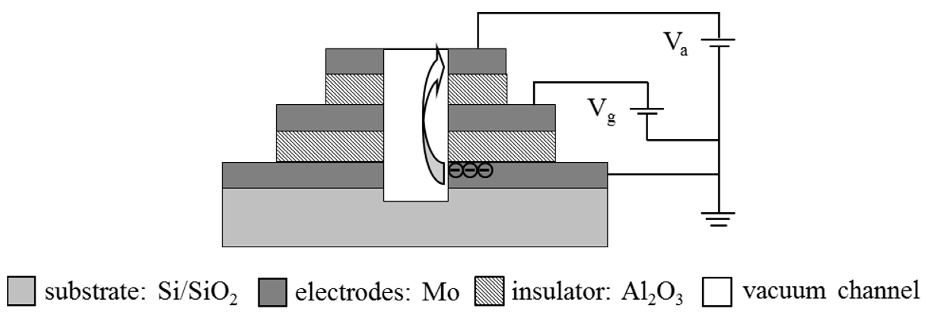
2.2. Structure
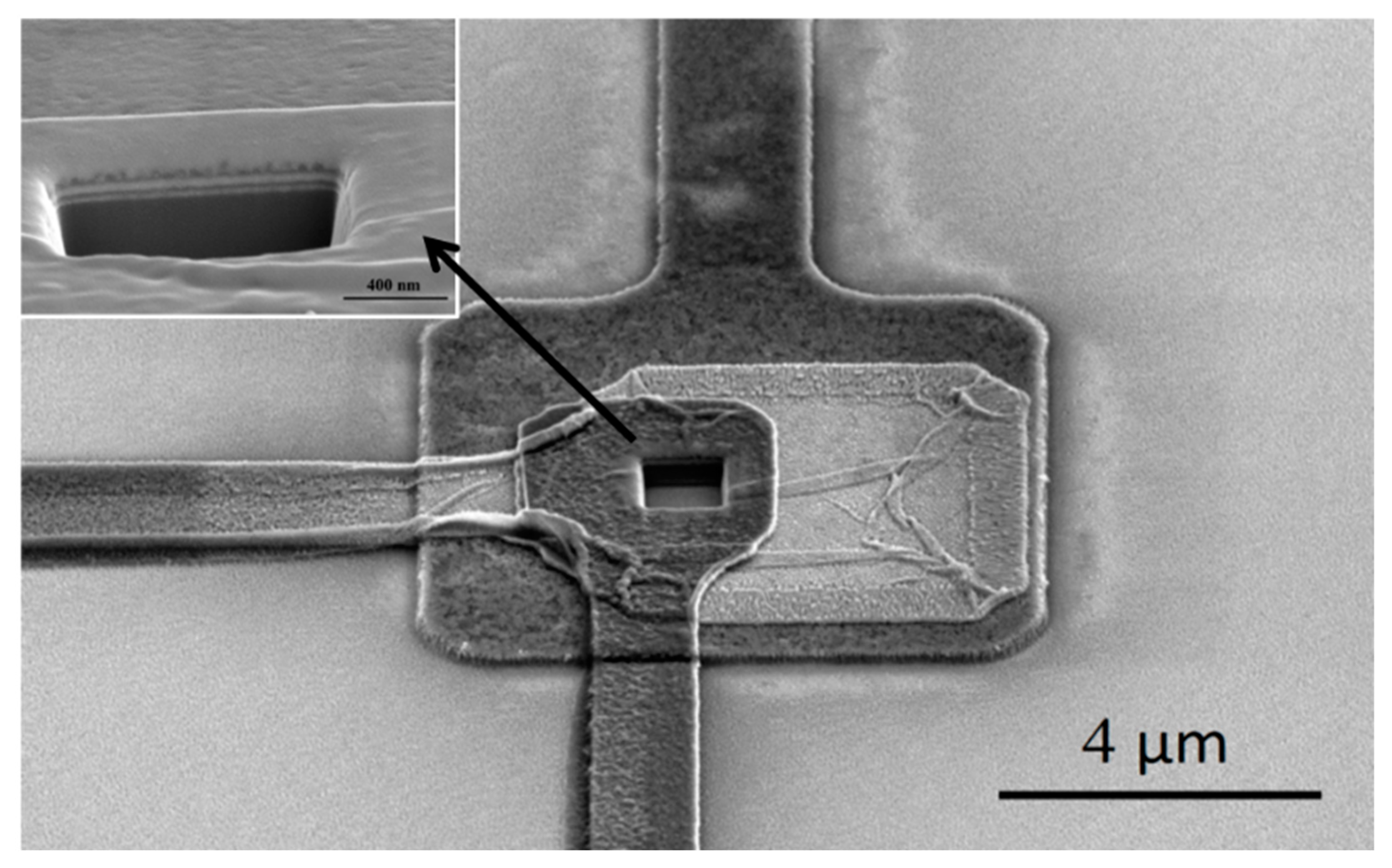
2.3. Fabrication
2.4. Characterization
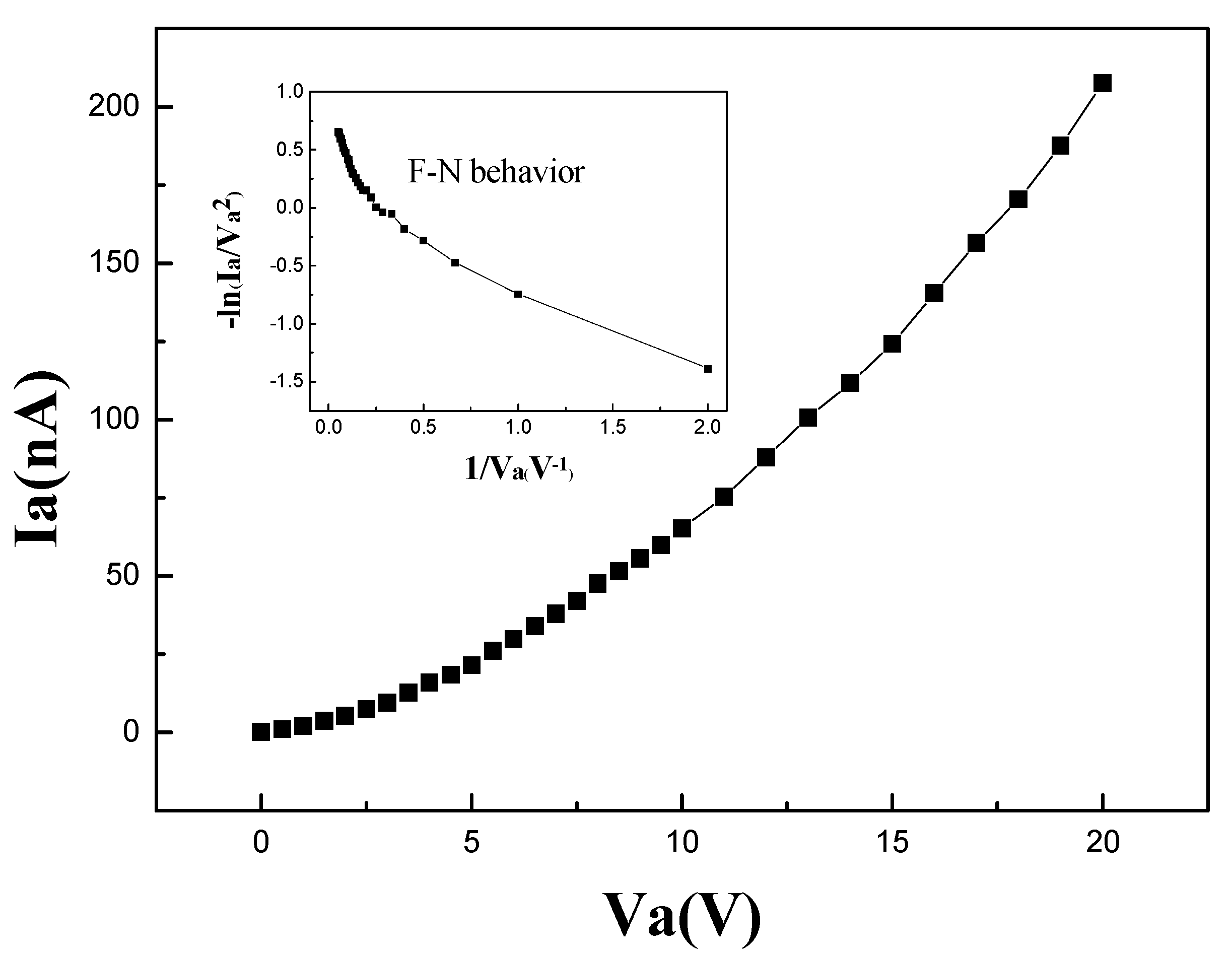
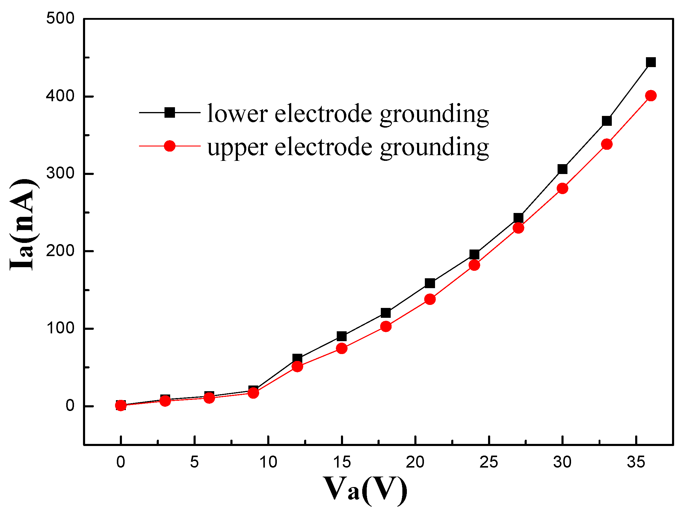
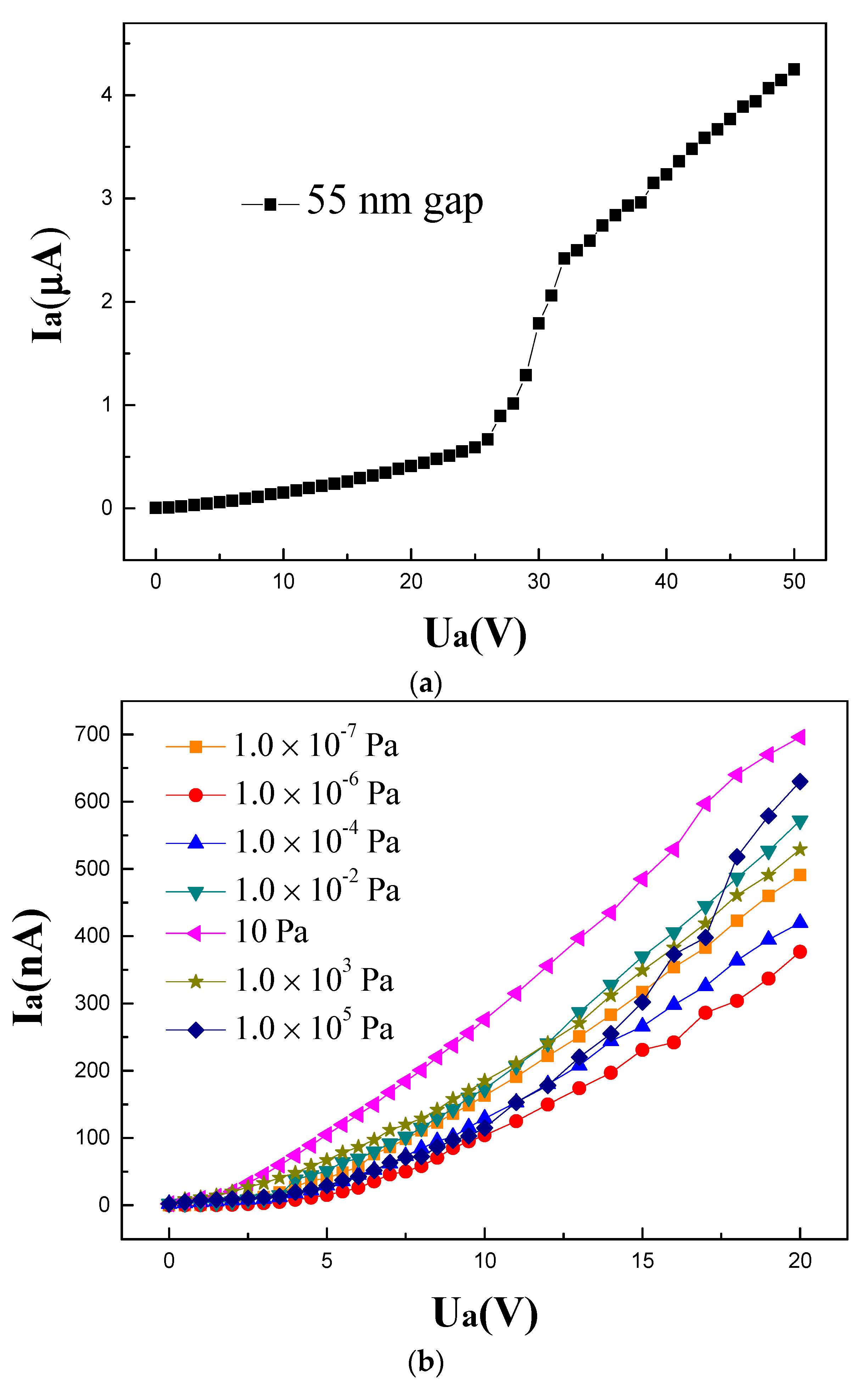
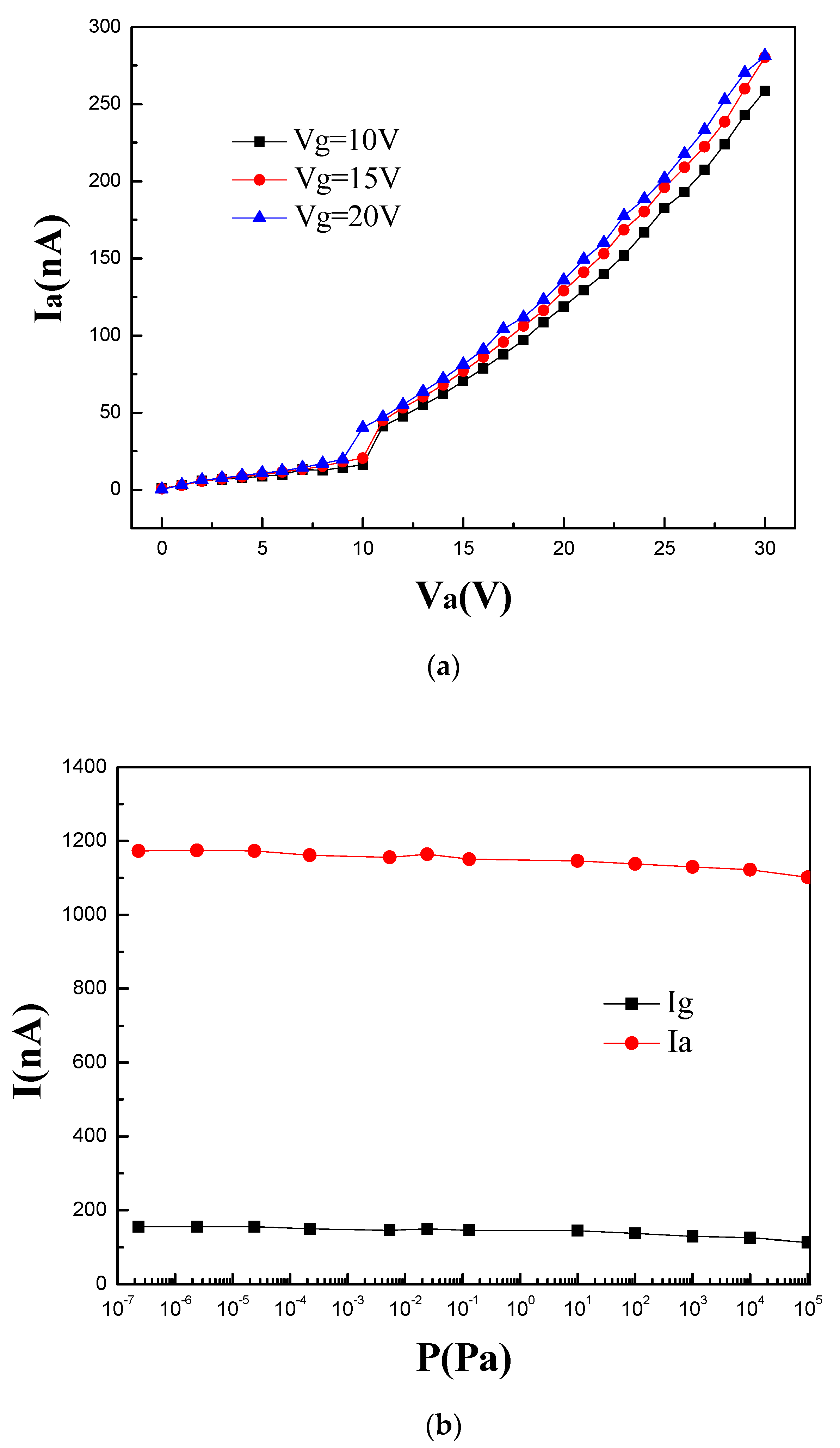
3. Results
4. Conclusions
Author Contributions
Funding
Data Availability Statement
Acknowledgments
Conflicts of Interest
References
- Spindt, C.A. A thin-film field-emission cathode. J. Appl. Phys. 1968, 39, 3504–3505. [Google Scholar] [CrossRef]
- Spindt, C.A.; Brodie, I.; Humphrey, L. Physical properties of thin-film field emission cathodes with molybdenum cones. J. Appl. Phys. 1976, 47, 5248–5263. [Google Scholar] [CrossRef]
- Whaley, D.R.; Duggal, R.; Armstrong, C.M.; Bellew, C.L.; Holland, C.E.; Spindt, C.A. 100 W operation of a cold cathode TWT. Trans. Electron. Devices 2009, 56, 896–905. [Google Scholar] [CrossRef]
- Pirio, G.; Legagneux, P.; Pribat, D.; Teo, K.B.K.; Chhowalla, M.; Amaratunga, G.A.J.; Milne, W.I. Fabrication and electrical characteristics of carbon nanotube field emission microcathodes with an intergrated gate electrode. Nanotechnology 2002, 13, 1. [Google Scholar] [CrossRef]
- Shao, W.; Ding, M.Q.; Chen, C.; Li, X.; Bai, G.; Feng, J.J. Micro-gated-field emission arrays with single carbon nanotubes grown on Mo tips. Appl. Surf. Sci. 2007, 252, 7559–7562. [Google Scholar] [CrossRef]
- Iemmo, L.; Bartolomeo, A.D.; Giubileo, F.; Luongo, G.; Passacantando, M.; Niu, G.; Hatami, F.; Skibitzki, O.; Schroeder, T. Graphene enhanced field emission from InP nanocrystals. Nanotechnology 2017, 28, 495705. [Google Scholar] [CrossRef] [Green Version]
- Schwierz, F. Graphene transistors: Status, prospects and problems. Proc. IEEE 2013, 101, 1567–1584. [Google Scholar] [CrossRef]
- Han, J.W.; Oh, J.S.; Meyyappan, M. Vacuum nanoelectronics: Back to the future?—Gate insulated nanoscale vacuum channel transistor. Appl. Phys. Lett. 2012, 100, 213505. [Google Scholar] [CrossRef] [Green Version]
- Srisonphan, S.; Jung, Y.S.; Kim, H.K. Metal-oxide-semiconductor field-effect transistor with a vacuum channel. Nat. Nanotech. 2012, 7, 504–508. [Google Scholar] [CrossRef]
- Park, I.J.; Jeon, S.G.; Shin, C. A New Slit-Type Vacuum-Channel Transistor. Trans. Electron. Devices 2014, 12, 4186–4191. [Google Scholar] [CrossRef]
- Han, J.W.; Moon, D.I.; Meyyappan, M. Nanoscale Vacuum Channel Transistor. Nano. Lett. 2017, 17, 2146–2151. [Google Scholar] [CrossRef] [PubMed]
- Stoner, B.R.; Glass, J.T. Nothing is like a vacuum. Nat. Nanotech. 2012, 7, 485–487. [Google Scholar] [CrossRef] [PubMed]
- Nirantar, S.; Ahmed, T.; Ren, G.; Gutruf, P.; Xu, C.; Bhaskaran, M.; Walia, S.; Sriram, S. Metal-Air Transistors: Semiconductor-free field-emission air-channel nanoelectronics. Nano. Lett. 2018, 18, 7478–7484. [Google Scholar] [CrossRef] [PubMed]
- Jennings, S.G. The mean free path in air. J. Aerosol. Sci. 1988, 19, 159–166. [Google Scholar] [CrossRef]
- Han, J.W.; Meyyappan, M. The device made of nothing. IEEE Spectr. 2014, 51, 30–35. [Google Scholar] [CrossRef]
- Bartolomeo, A.D.; Giubileo, F.; Iemmo, L.; Romeo, F.; Russo, S.; Unal, S.; Passacantando, M.; Grossi, V.; Cucolo, A.M. Leakage and field emission in side-gate grapheme field effect transistors. Appl. Phys. Lett. 2016, 109, 023510. [Google Scholar] [CrossRef] [Green Version]
- Sapkota, K.R.; Leonard, F.; Talin, A.A.; Gunning, B.P.; Kazanowska, B.A.; Jones, K.S.; Wang, G.T. Ultralow voltage GaN vacuum nanodiodes in air. Nano. Lett. 2021, 21, 1928–1934. [Google Scholar] [CrossRef]
- Chang, W.T.; Hsu, H.J.; Pao, P.H. Vertical field emission air-channel diodes and transistors. Micromachines 2019, 10, 858. [Google Scholar] [CrossRef] [Green Version]
- Feng, J.J.; Li, X.H.; Hu, J.N.; Cai, J. General vacuum electronics. J. Electromagn. Eng. Sc. 2020, 20, 1–8. [Google Scholar] [CrossRef]
- Han, J.W.; Seol, M.L.; Meyyappan, M. A nanoscale vacuum field emission gated diode with an umbrella cathode. Nanoscale Adv. 2021, 3, 1725–1729. [Google Scholar] [CrossRef]
- Han, J.W.; Seol, M.L.; Moon, D.I.; Hunter, G.; Meyyappan, M. Nanoscale vacuum channel transistors fabricated on silicon carbide wafers. Nat. Electron. 2019, 2, 405–411. [Google Scholar] [CrossRef]
- Kim, H.K. Vacuum transistors for space travel. Nat. Electron. 2019, 2, 374–375. [Google Scholar] [CrossRef]


Disclaimer/Publisher’s Note: The statements, opinions and data contained in all publications are solely those of the individual author(s) and contributor(s) and not of MDPI and/or the editor(s). MDPI and/or the editor(s) disclaim responsibility for any injury to people or property resulting from any ideas, methods, instructions or products referred to in the content. |
© 2023 by the authors. Licensee MDPI, Basel, Switzerland. This article is an open access article distributed under the terms and conditions of the Creative Commons Attribution (CC BY) license (https://creativecommons.org/licenses/by/4.0/).
Share and Cite
Han, P.; Li, X.; Cai, J.; Feng, J. Vertical Nanoscale Vacuum Channel Triodes Based on the Material System of Vacuum Electronics. Micromachines 2023, 14, 346. https://doi.org/10.3390/mi14020346
Han P, Li X, Cai J, Feng J. Vertical Nanoscale Vacuum Channel Triodes Based on the Material System of Vacuum Electronics. Micromachines. 2023; 14(2):346. https://doi.org/10.3390/mi14020346
Chicago/Turabian StyleHan, Panyang, Xinghui Li, Jun Cai, and Jinjun Feng. 2023. "Vertical Nanoscale Vacuum Channel Triodes Based on the Material System of Vacuum Electronics" Micromachines 14, no. 2: 346. https://doi.org/10.3390/mi14020346