Article

Low Trapping Effects and High Electron Confinement in Short AlN/GaN-On-SiC HEMTs by Means of a Thin AlGaN Back Barrier

CNRS-IEMN, Institute of Electronic, Microelectronic and Nanotechnology, 59652 Villeneuve-d’Ascq, France
*
Authors to whom correspondence should be addressed.
Micromachines 2023, 14(2), 291; https://doi.org/10.3390/mi14020291
Submission received: 4 January 2023 / Revised: 19 January 2023 / Accepted: 20 January 2023 / Published: 22 January 2023

Abstract

:
In this paper, we report on an enhancement of mm-wave power performances with a vertically scaled AlN/GaN heterostructure. An AlGaN back barrier is introduced underneath a non-intentionally doped GaN channel layer, enabling the prevention of punch-through effects and related drain leakage current under a high electric field while using a moderate carbon concentration into the buffer. By carefully tuning the Al concentration into the back barrier layer, the optimized heterostructure offers a unique combination of electron confinement and low trapping effects up to high drain bias for a gate length as short as 100 nm. Consequently, pulsed (CW) Load-Pull measurements at 40 GHz revealed outstanding performances with a record power-added efficiency of 70% (66%) under high output power density at VDS = 20 V. These results demonstrate the interest of this approach for future millimeter-wave applications.

1. Introduction

In recent decades, remarkable progress has been achieved with GaN high electron mobility transistors (HEMTs) for use in high frequency power amplification and switching applications. Recent progress has allowed the demonstration of high RF performance up to Ka-band [1,2,3,4,5,6]. However, at a higher frequency, the efficiency and robustness of GaN HEMTs, especially under high drain bias above 15 V, are still limited due to enhanced trapping effects, reduced electron confinement and self-heating when downscaling the device size. Currently, the most matured GaN HEMTs are based on a AlGaN/GaN heterostructure [6,7,8,9,10]. More recently, Al-rich ultrathin sub-10 nm barrier heterostructures have received much attention for millimeter-wave applications [11,12,13,14,15,16,17,18,19,20,21,22]. This is because they can deliver significantly higher 2DEG sheet carrier density compared to AlGaN/GaN HEMTs while offering the possibility to highly scale the epitaxial structure as needed when using short gate lengths [23,24,25]. Therefore, further reducing the gate length to reach a higher frequency of operation requires significant changes of standard epitaxial materials and device design, such as self-aligned gates and an AlGaN back barrier [26,27]. Breakthrough technologies are needed to achieve simultaneously high efficiency under high output power, together with high reliability. A number of new device designs have been developed in this frame, including graded channel HEMTs [28,29] and N-polar HEMT [30,31,32] showing attractive performances in Ka-band and above. In order to further push the performance limits of mm-wave ultrashort GaN transistors, the electron confinement and trapping effects under a high electric field must be optimized. This requires extensive buffer engineering. Recently, we evaluated the impact of various carbon-doping concentrations into the buffer with different undoped GaN channel thickness on the device performance [33]. It was shown that a thin GaN channel, typically below 150 nm, combined with a high carbon concentration into the buffer leads not only to a high electron confinement under high drain bias for 100 nm GaN transistors, but also low leakage current at the expense of trapping effects.
In this work, we insert a thin AlGaN back barrier between a moderately carbon-doped buffer and an undoped GaN channel with the aim of overcoming the trade-off between the electron trapping and the electron confinement, enabling superior bias operation and performances for 100 nm AlN/GaN HEMTs. An extensive Al-content variation has been performed in the back barrier with the aim of optimizing the related polarization and preventing punch-through effects under a high electric field.

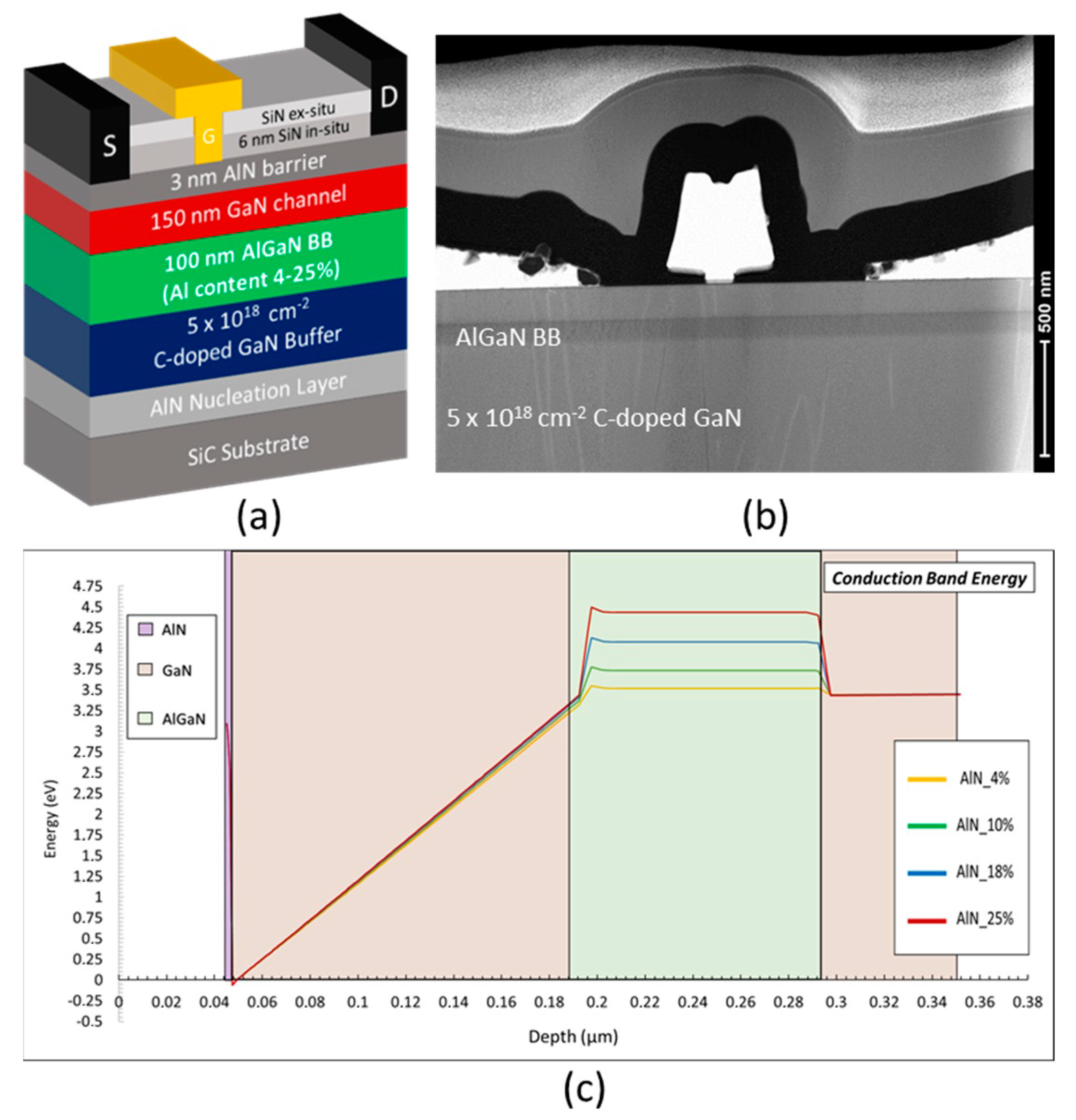
2. Device Technology

Figure 1a shows a schematic cross-section of HEMT structure grown by metal organic chemical vapor deposition (MOCVD) on 4 in. SiC substrates. A total of four structures have been realized, consisting of an AlN nucleation layer and a 5 × 1018 cm−3 carbon-doped GaN buffer allowing significantly reduced trapping effects when located away from the channel [33]. This is followed by a 100 nm AlGaN back barrier layer with an Al-content varying from 4% to 25% in order to evaluate the impact on the electron confinement. A 150 nm undoped GaN channel and a 3 nm AlN barrier layer are then used to benefit from both a high polarization and a favorable aspect ratio gate length to gate-to-channel distance in order to mitigate the short channel effects with short gate lengths. Finally, the structures were capped with a 6 nm in situ SiN layer to passivate the surface states and thus avoid DC to RF dispersion.
The source drain ohmic contacts have been formed by a Ti/Al/Ni/Au metal stack annealed at 850 °C directly on top of the AlN barrier by etching the in situ Si3N4 layer. Ni/Au T-gates with various gate lengths from 100 nm to 250 nm were then defined by e-beam lithography. Figure 1b shows a Transmission Electron Microscopy (TEM) view of the HEMT structure depicting the epitaxial stack as well as the ohmic and Schottky contacts. A 200 nm PECVD Si3N4 layer was deposited as final passivation. Hall measurements at room temperature show a 2DEG concentration ns ∼ 2 × 1013 cm−2 with an electron mobility ∼ 950 cm2 V−1·s−1 and a sheet resistance Rsheet∼ 300 Ω/◻, which is similar for all structures.
The structure variation of the Al-content from 4% to 25% in the AlGaN back barrier is labelled as follows: Al-4%, Al-10%, Al-18% and Al-25%. The energy band diagrams of the structures appear in Figure 1c, showing the increased polarization resulting from a higher Al-content into the back barrier.

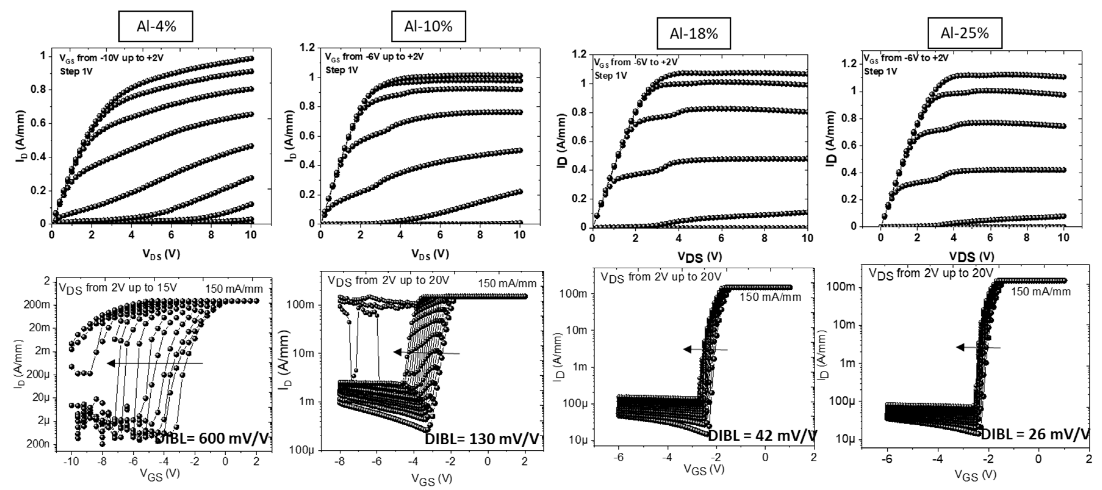
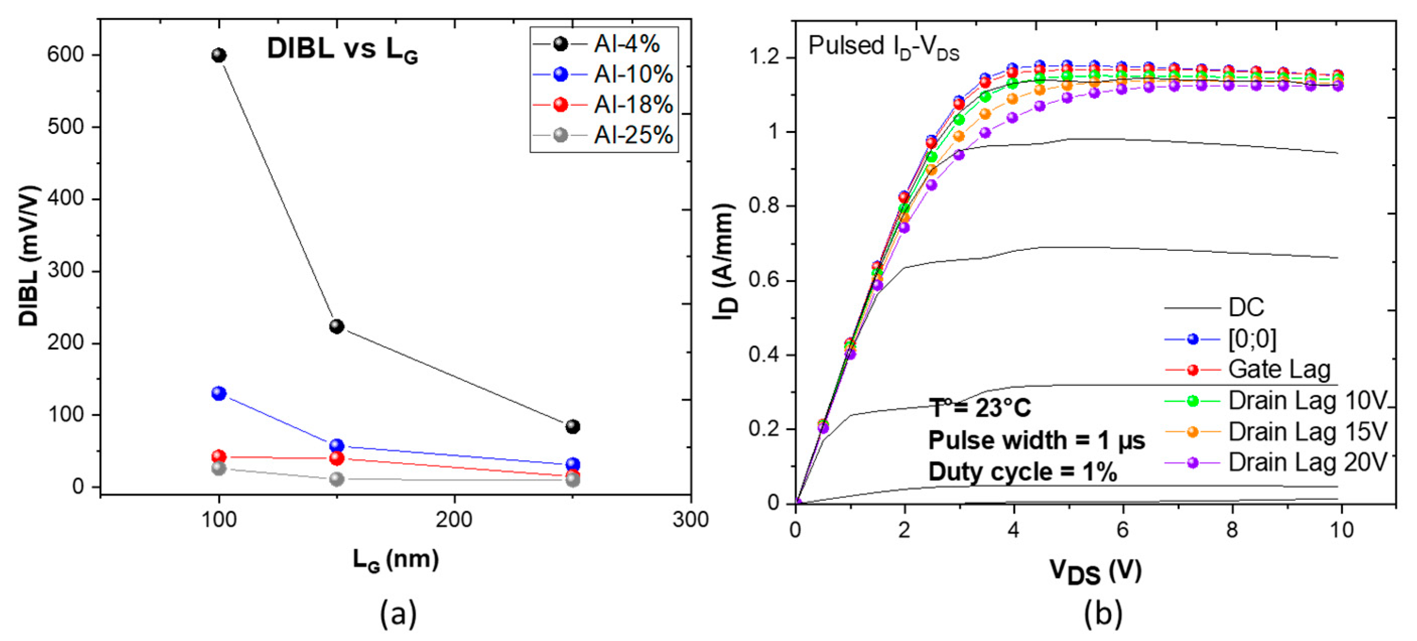
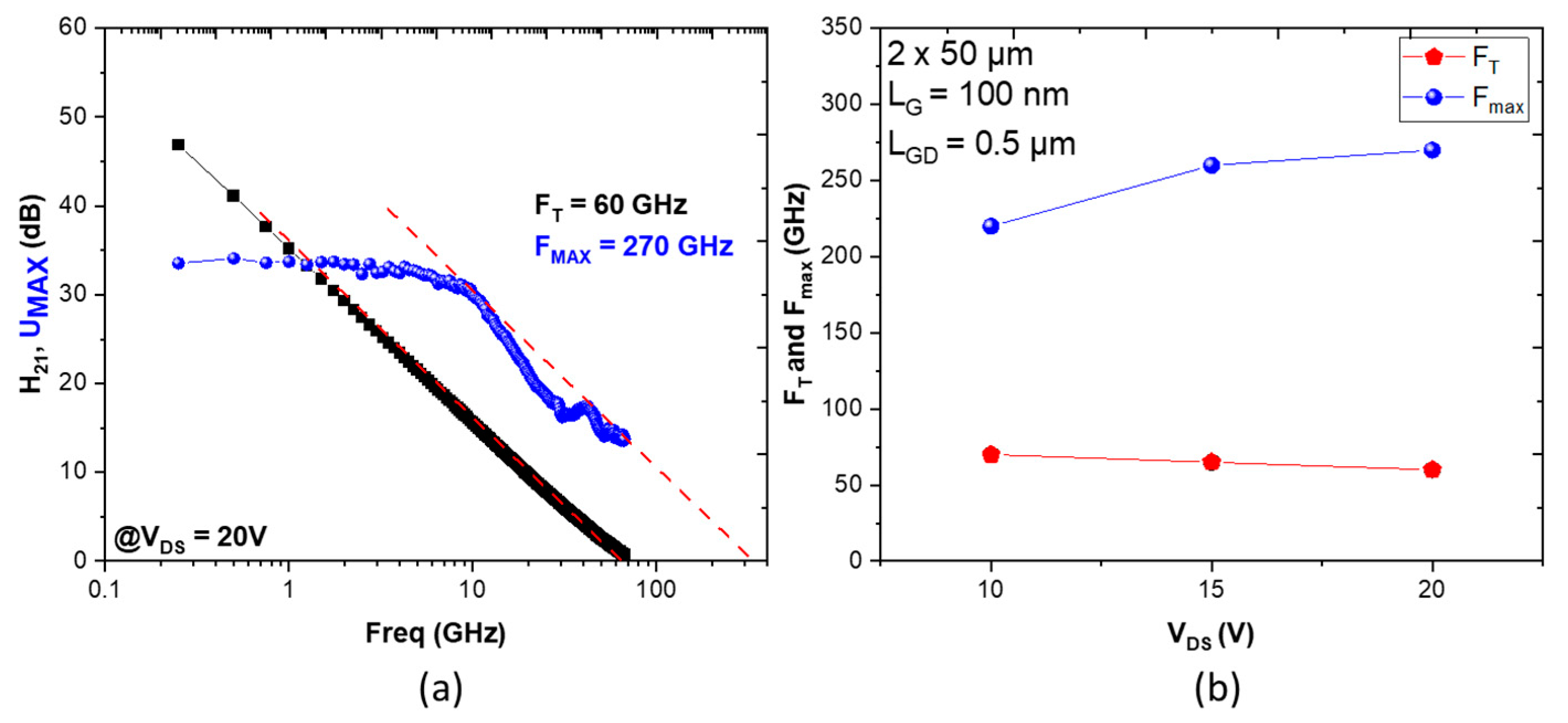
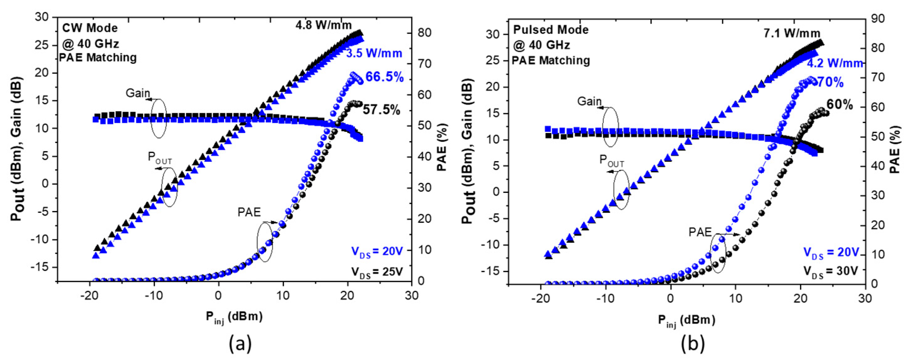
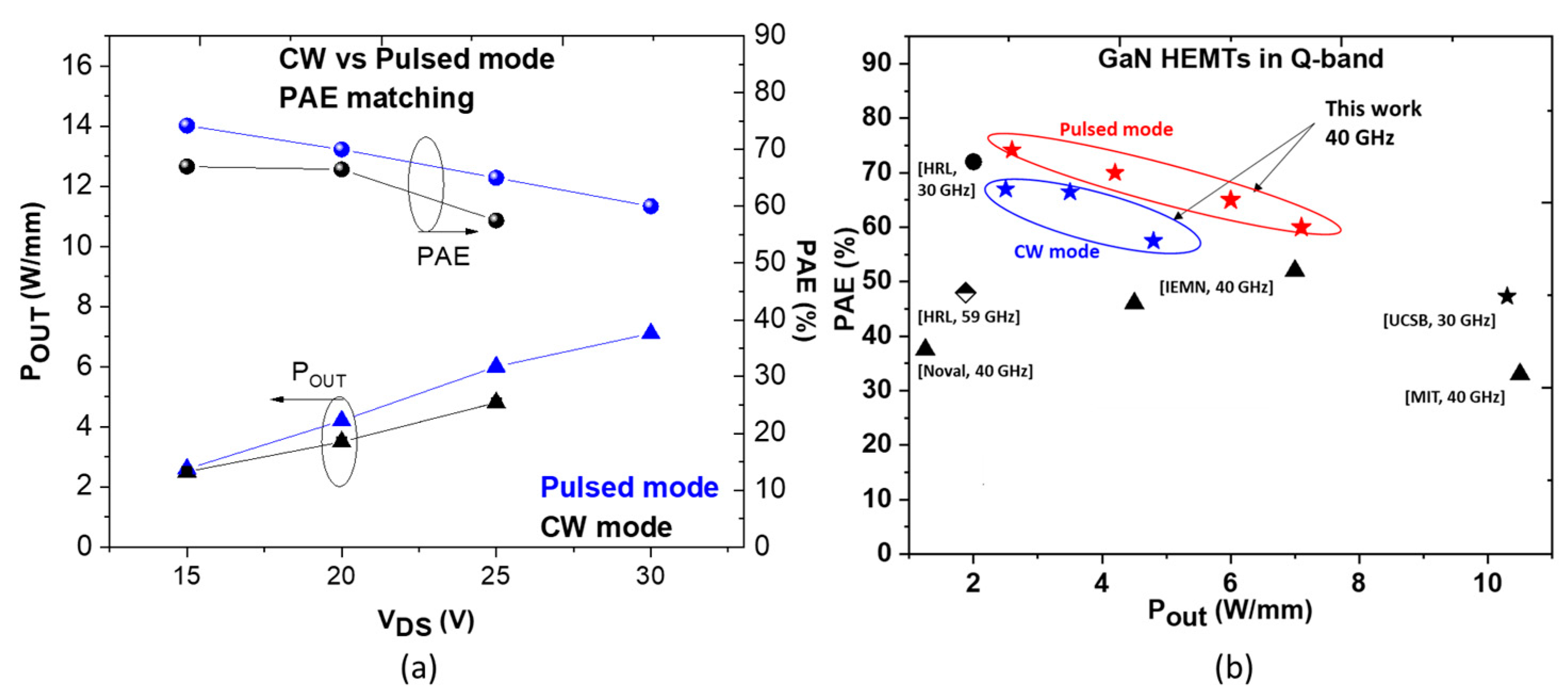
3. DC and RF Characterization

DC measurements have been performed using a Keysight A2902A static modular and source monitor. Figure 2 shows the output and transfer characteristics of each structure, with a compliance fixed at 150 mA/mm and swept from VDS = 2 V up to 20 V in order to extract the drain bias-induced barrier lowering (DIBL), which is a key parameter for evaluating the 2DEG electron confinement. This required 2 × 50 µm transistors with a gate length of 100 nm and a gate-to-drain distance (LGD) of 0.5 µm to be measured on the different structures, Al-4%, Al-10%, Al-18% and Al-25%. The output characteristics show a maximum rain current of approximately 1 A/mm on all structures, which confirms the similarity of the 2DEG density. For the structure Al-4%, we observed a severe degradation of the electron confinement, which is reflected by a large DIBL of 600 mV/V as well as a strong increase of the off-state leakage current. The degradation of the electron confinement is attributed to the low Al-content of 4% in the AlGaN back barrier, for which the back polarization is not high enough to prevent electron injection into the buffer layers under such a high electric field. Therefore, similar structures with a higher Al-content in the back barrier have been tested in order to enhance the electron confinement with short gate lengths. The structure Al-10% indeed shows a drastic improvement of the electron confinement, by a factor of 4, in terms of the DIBL parameter decreasing from 600 mV/V for the structure Al-4% to 130 mV/V for the structure Al-10%. As expected, further increasing the Al-content in the AlGaN back barrier up to 18% and 25% results in a gradual enhancement of the electron confinement, especially the Al-25% structure with a much lower DIBL of less than 30 mV/V for 100 nm gate lengths while maintaining low drain leakage current and high robustness up to VDS = 20 V.
It can be noted that larger gate lengths were measured in the same way. Figure 3a depicts the DIBL as a function of the gate length for each structure. The systematic degradation of the electron confinement is clearly confirmed with short gate lengths (sub-150 nm) when using low Al-content in the AlGaN back barrier (e.g., 4% and 10%). On the other hand, the structures with sufficient Al-content (e.g., >18%) show excellent electron confinement down to 100 nm gate length while maintaining low leakage current and high robustness under a high electric field (VDS > 15 V).
Pulsed ID–VDS characteristics at room temperature revealing the current collapse when using various quiescent bias points appear in Figure 3b. The specific pulsed I–V protocol based on I–V characteristics has been settled with the following quiescent bias points: cold point at (VGQ = 0 V, VDQ = 0 V), gate lag at (VGQ = −4 V, VDQ = 0 V) and drain lag at (VGQ = −4 V, VDQ = 10 V, 15 V and 20 V) using a pulsed width of 1 μs and a duty cycle of 1%. This required 2 × 50 µm transistors with LG of 100 nm and LGD of 0.5 µm to be measured, which showed low trapping effects owing to the moderate carbon concentration of 5 × 1018 cm−2 located 250 nm away from the 2DEG as well as the excellent electron confinement. Indeed, a correlation between an enhanced electron confinement owing to the use of a back barrier and a reduction of electron trapping has been demonstrated [34].
Figure 4 shows S-parameters measured on the structure Al-25% from 250 MHz to 67 GHz using a Rhode and Schwarz ZVA67GHz network analyzer. The current gain extrinsic cut-off frequency (FT) slightly decreases with VDS as expected. On the other hand, the maximum oscillation frequency (Fmax) increases as a function of VDS, which further confirms the reduced trapping (Figure 4b). FT/Fmax of 60/270 GHz is achieved at VDS = 20 V for a 2 × 50 µm with LG of 100 nm and LGD of 0.5 µm (Figure 4a). The small signal power gain measured at 40 GHz is as high as 17 dB.

4. Large Signal Characterization

In order to further validate the benefit of low trapping effects combined with an excellent electron confinement under a high electric field, continuous-wave (CW) and pulsed Load-Pull measurements have been performed on 100 nm transistors from the structure A1-25% at 40 GHz. Details of the power bench used for these measurements can be found in [35]. Figure 5a shows CW PAE and POUT as a function of the injected power (Pinj) of a 2 × 50 µm AlN/GaN transistor with LG = 100 nm and LGD = 0.5 µm measured in deep class AB at VDS = 20 V and 25 V. A state-of-the-art PAE above 65% associated with a POUT of 3.5 W/mm is obtained for an optimum matching PAE. At VDS = 25 V, POUT increases as expected up to 4.8 W/mm with a peak PAE of 57.5%. It can be noted that the drop of PAE as a function of VDS is mainly due to self-heating.
Figure 5b shows the power performances using the same device in pulsed mode (pulse width of 1 μs and duty cycle of 1%). An outstanding PAE of 70% is measured with a corresponding POUT of 4.2 W/mm at VDS = 20 V. This heterostructure enables superior drain bias operation up to VDS = 30 V while maintaining high PAE of approximately 60% under a significant POUT of 7.1 W/mm.
Figure 6a shows a summary of the power performance as a function of drain bias, revealing a rather small gap between CW and pulsed mode. This translates the low trapping effects and enhanced electron confinement under high drain bias at 40 GHz. Figure 6b depicts a benchmark of GaN HEMTs representing the PAE as a function of POUT from Ka to Q-band. Both CW and pulsed RF power performances appear to be favorably comparable to state-of-the-art GaN HEMTs, reflecting the significant interest in this technology for millimeter-wave applications. For instance, to the best of our knowledge, a PAE > 65% combined with a POUT > 3 W/mm at 40 GHz in CW is demonstrated for the first time.

5. Conclusions

In this work, we evaluated the insertion of a thin AlGaN back barrier with an extensive Al-content variation (from 4% to 25%), with the aim of pushing the limits in terms of drain bias operation of AlN/GaN HEMTs with short gate lengths (down to 100 nm) while maintaining low trapping effects. A higher Al-content in the AlGaN back barrier shows an excellent electron confinement together with low trapping effects despite the significant electric field generated by the short gate length under high drain bias (>20 V). Large signal performances at 40 GHz revealed state-of-the-art power performances for the structure using 25% Al-content in the AlGaN back barrier combined with a moderately carbon-doped GaN buffer. This technology paves the way for highly efficient mm-wave GaN HEMTs delivering superior output power density as needed for next-generation RF power devices.

Author Contributions

Device design, K.H., S.V., L.B.-H., F.G., E.O. and F.M.; fabrication, K.H., S.V., L.B.-H., F.G., E.O. and F.M.; characterization, K.H., S.V., L.B.-H., F.G., E.O. and F.M.; writing—original draft preparation, K.H., S.V., L.B.-H., F.G., E.O. and F.M. All authors have read and agreed to the published version of the manuscript.

Funding

This research was funded by the national program LABEX GANEX (ANR-11-LABX-0014) and the French Defense Procurement Agency (DGA) under the project called GREAT.

Data Availability Statement

Not applicable.

Acknowledgments

The authors would like to acknowledge the company SOITEC Belgium for high-quality material delivery and the support of the French RENATECH network.

Conflicts of Interest

The authors declare no conflict of interest. The funders had no role in the design of the study; in the collection, analyses, or interpretation of data; in the writing of the manuscript; or in the decision to publish the results.

References

  1. Romanczyk, B.; Wienecke, S.; Guidry, M.; Li, H.; Ahmadi, E.; Zheng, X.; Keller, S.; Mishra, U.K. Demonstration of Constant 8 W/Mm Power Density at 10, 30, and 94 GHz in State-of-the-Art Millimeter-Wave N-Polar GaN MISHEMTs. IEEE Trans. Electron. Devices 2018, 65, 45–50. [Google Scholar] [CrossRef]
  2. Moon, J.S.; Wong, D.M.; Hu, P.; Hashimoto, M.; Antcliffe, C.; McGuire, M.M.; Willadson, P. 55% PAE and High Power Ka-Band GaN HEMTs Source Contact Ledge. EDL IEEE 2008, 29, 834–837. [Google Scholar] [CrossRef]
  3. Crespo, A.; Bellot, M.M.; Chabak, K.D.; Gillespie, J.K.; Jessen, G.H.; Miller, V.; Trejo, M.; Via, G.D.; Walker, D.E.; Winningham, B.W. High-Power Ka-Band Performance of AlInN/GaN. EDL IEEE 2010, 31, 8–10. [Google Scholar] [CrossRef]
  4. Moon, J.S.; Wu, S.; Wong, D.; Milosavljevic, I.; Conway, A.; Hashimoto, P.; Hu, M.; Antcliffe, M.; Micovic, M. Gate-Recessed AlGaN—GaN HEMTs for High-Performance Millimeter-Wave Applications. IEEE Electron. Device Lett. 2005, 26, 348–350. [Google Scholar] [CrossRef]
  5. Palacios, T.; Chakraborty, A.; Rajan, S.; Poblenz, C.; Keller, S.; DenBaars, S.P.; Speck, J.S.; Mishra, U.K. High-Power AlGaN/GaN HEMTs For. IEEE Electron. Device Lett. 2005, 26, 8–11. [Google Scholar] [CrossRef] [Green Version]
  6. Bouslama, M.; Gillet, V.; Chang, C.; Nallatamby, J.C.; Sommet, R.; Prigent, M.; Quere, R.; Lambert, B. Dynamic Performance and Characterization of Traps Using Different Measurements Techniques for the New AlGaN/GaN HEMT of 0.15- Μm Ultrashort Gate Length. IEEE Trans. Microw. Theory Tech. 2019, 67, 2475–2482. [Google Scholar] [CrossRef]
  7. Wu, Y.; Saxler, A.; Moore, M.; Smith, R.P.; Sheppard, S.; Chavarkar, P.M.; Wisleder, T.; Mishra, U.K.; Parikh, P. 30-W/mm GaN HEMTs by Field Plate Optimization. IEEE Electron. Device Lett. 2004, 25, 117–119. [Google Scholar] [CrossRef]
  8. Ambacher, O.; Smart, J.; Shealy, J.R.; Weimann, N.G.; Chu, K.; Murphy, M.; Schaff, W.J.; Eastman, L.F.; Dimitrov, R.; Wittmer, L. Two-Dimensional Electron Gases Induced by Spontaneous and Piezoelectric Polarization Charges in N- and Ga-Face AlGaN/GaN Heterostructures. J. Appl. Phys. 1999, 85, 3222–3233. [Google Scholar] [CrossRef] [Green Version]
  9. Wu, Y.-F.; Moore, M.; Saxler, A.; Wisleder, T.; Parikh, P. 40-W/mm Double Field-Plated GaN HEMTs. 64th Device Res. Conf. Conf. Dig. DRC 2006, 151–152. [Google Scholar]
  10. Sun, Y.; Zhang, H.; Yang, L.; Hu, K.; Xing, Z.; Liang, K.; Yu, H.; Fang, S.; Kang, Y.; Wang, D.; et al. Correlation Between Electrical Performance and Gate Width of GaN-Based HEMTs. IEEE Electron. Device Lett. 2022, 1199, 1202. [Google Scholar] [CrossRef]
  11. Margomenos, A.; Kurdoghlian, A.; Micovic, M.; Shinohara, K.; Brown, D.F.; Corrion, A.L.; Moyer, H.P.; Burnham, S.; Regan, D.C.; Grabar, R.M. GaN Technology for E, W and G-Band Applications. IEEE Compd. Semicond. Integr. Circuit Symp. 2014, 1–4. [Google Scholar] [CrossRef]
  12. Schwantuschke, D.; Godejohann, B.J.; Brückner, P.; Tessmann, A.; Quay, R. mm-Wave Operation of AlN/GaN-Devices and MMICs at V- & W-Band. IEEE Int. Microw. Radar Conf. 2018, 238–241. [Google Scholar] [CrossRef]
  13. Kohn, E.; Medjdoub, F. InAlN—A New Barrier Material for GaN-Based HEMTs. In Proceedings of the International Workshop on The Physics of Semiconductor Devices, New Delhi, Indian, 17–20 December 2007; Volume 6, pp. 311–316. [Google Scholar] [CrossRef]
  14. Kabouche, R.; Derluyn, J.; Pusche, R.; Degroote, S.; Germain, M.; Pecheux, R.; Okada, E.; Zegaoui, M.; Medjdoub, F. Comparison of C-Doped AlN/GaN HEMTs and AlN/GaN/AlGaN Double Heterostructure for MmW Applications. In Proceedings of the 13th European Microwave Integrated Circuits Conference (EuMIC), Madrid, Spain, 23–25 September 2018; pp. 5–8. [Google Scholar] [CrossRef]
  15. Godejohann, B.J.; Ture, E.; Müller, S.; Prescher, M.; Kirste, L.; Aidam, R.; Polyakov, V.; Brückner, P.; Breuer, S.; Köhler, K. AlN/GaN HEMTs Grown by MBE and MOCVD: Impact of Al Distribution. Phys. Status Solidi Basic Res. 2017, 254, 3–7. [Google Scholar] [CrossRef]
  16. Dogmus, E.; Kabouche, R.; Linge, A.; Okada, E.; Zegaoui, M.; Medjdoub, F. High Power, High PAE Q-Band Sub-10 nm Barrier Thickness AlN/GaN HEMTs. Phys. Status Solidi Appl. Mater. Sci. 2017, 214, 797. [Google Scholar] [CrossRef] [Green Version]
  17. Shinohara, K.; Corrion, A.; Regan, D.; Milosavljevic, I.; Brown, D.; Burnham, S.; Willadsen, P.J.; Butler, C.; Schmitz, A.; Wheeler, D. 220GHz f T and 400GHz f Max in 40-nm GaN DH-HEMTs with Re-Grown Ohmic. Int. Electron. Devices Meet. 2010, 30.1.1–30.1.4. [Google Scholar] [CrossRef]
  18. Tang, Y.; Shinohara, K.; Regan, D.; Corrion, A.; Brown, D.; Wong, J.; Schmitz, A.; Fung, H.; Kim, S.; Micovic, M. Ultrahigh-Speed GaN High-Electron-Mobility Transistors with FT/Fmax of 454/444 GHz. IEEE Electron. Device Lett. 2015, 36, 549–551. [Google Scholar] [CrossRef]
  19. Cwiklinski, M.; Bruckner, P.; Leone, S.; Friesicke, C.; Lozar, R.; Mabler, H.; Quay, R.; Ambacher, O. 190-GHz G-Band GaN Amplifier MMICs with 40GHz of Bandwidth. IEEE MTT-S Int. Microw. Symp. Dig. 2019, 2019, 1257–1260. [Google Scholar] [CrossRef]
  20. Medjdoub, F.; Zegaoui, M.; Linge, A.; Grimbert, B.; Silvestri, R.; Meneghini, M.; Meneghesso, G.; Zanoni, E. High PAE High Reliability AlN/GaN Double Heterostructure. Solid State Electron. 2015, 113, 49–53. [Google Scholar] [CrossRef]
  21. Medjdoub, F.; Zegaoui, M.; Rolland, N. Beyond 100GHz AlN/GaN HEMTs on Silicon Substrate. Electron. Lett. 2011, 47, 1345–1346. [Google Scholar] [CrossRef]
  22. Angelotti, A.M.; Gibiino, G.P.; Santarelli, A.; Corrado, F. Experimental Characterization of Charge Trapping Dynamics in 100-nm AlN/GaN/AlGaN-on-Si HEMTs by Wideband Transient Measurements. IEEE Transac. Electron. Devices 2020, 67, 3069–3074. [Google Scholar] [CrossRef]
  23. Harrouche, K.; Kabouche, R.; Okada, E.; Medjdoub, F. High Performance and Highly Robust AlN/GaN HEMTs for Millimeter-Wave Operation. IEEE J. Electron. Devices Soc. 2019, 7, 314. [Google Scholar] [CrossRef]
  24. Gao, Z.H.; Meneghini, M.; Harrouche, K.; Kabouche, R.; Chiocchetta, F.; Okada, E.; Rampazzo, F.; De Santi, C.; Medjdoub, F.; Meneghesso, G. Short Term Reliability and Robustness of Ultra-Thin Barrier, 110 nm-Gate AlN/GaN HEMTs. Microelectron. Reliab. 2021, 123, 114199. [Google Scholar] [CrossRef]
  25. Harrouche, K.; Kabouche, R.; Okada, E.; Medjdoub, F. High Power AlN/GaN HEMTs with Record Power-Added-Efficiency >70% at 40 GHz. In Proceedings of the IEEE MTT-S International Microwave Symposium (IMS), Los Angeles, CA, USA, 4–6 August 2020. [Google Scholar]
  26. Shinohara, K.D.; Regan, I.; Milosavljevic, A.; Corrion, L.D.; Brown, F.P.; Willadsen, J.C.; Butler, A.; Schmitz, S.; Kim, V.; Lee, A.; et al. Electron Velocity Enhancement in Laterally Scaled GaN DH-HEMTs With fT of 260 GHz. IEEE Electron. Device Lett. 2011, 32, 1074–1076. [Google Scholar] [CrossRef]
  27. Micovic, M.; Hashimoto, P.; Hu, M.; Milosavljevic, I.; Duvall, J.; Peter, J.; Willadsen, W.-S.; Wong, A.; Conway, M.; Kurdoghlian, A.; et al. GaN Double Heterojunction Field Effect Transistor For Microwave and Millimeterwave Power Applications. In Proceedings of the IEEE International Electron Devices Meeting, San Francisco, CA, USA, 13–15 December 2004; pp. 807–810. [Google Scholar] [CrossRef]
  28. Moon, J.S.; Grabar, R.; Wong, J.; Antcliffe, M.; Chen, P.; Arkun, E.; Khalaf, I.; Corrion, A.; Chappell, J. High-speed Graded-channel AlGaN GaN HEMTs with Power Added Efficiency 70% at 30 GHz. Electron. Lett. 2020, 56, 678–680. [Google Scholar] [CrossRef]
  29. Moon, J.; Wong, J.; Grabar, B.; Antcliffe, M.; Chen, P.; Arkun, E.; Khalaf, I.; Corrion, A. High-Speed Linear GaN Technology with a Record Efficiency in Ka-Band. In Proceedings of the EUMW Conference, Paris, France, 30 September–4 October 2019. [Google Scholar]
  30. Romanczyk, B.; Guidry, M.; Zheng, X.; Shrestha, P.; Li, H.; Ahmadi, E.; Keller, S.; Mishra, U.K. Evaluation of Linearity at 30 GHz for N-Polar GaN Deep Recess Transistors with 10.3 W/Mm of Output Power and 47.4% PAE. Appl. Phys. Lett. 2021, 119, 587. [Google Scholar] [CrossRef]
  31. Liu, W.; Romanczyk, B.; Guidry, M.; Hatui, N.; Wurm, C.; Li, W.; Shrestha, P.; Zheng, X.; Keller, S.; Mishra, U.K. 6.2 W/Mm and Record 33.8% PAE at 94 GHz from N-Polar GaN Deep Recess MIS-HEMTs with ALD Ru Gates. IEEE Microw. Wirel. Compon. Lett. 2021, 31, 748–751. [Google Scholar] [CrossRef]
  32. Wienecke, S.; Romanczyk, B.; Guidry, M.; Li, H.; Ahmadi, E.; Hestroffer, K.; Zheng, X.; Keller, S.; Mishra, U.K. N-Polar GaN Cap MISHEMT With Record Power Density Exceeding 6.5 W/mm at 94 GHz. IEEE Electron. Device Lett. 2017, 38, 359–362. [Google Scholar] [CrossRef]
  33. Harrouche, K.; Venkatachalam, S.; Grandpierron, F.; Okada, E.; Medjdoub, F. Impact of Undoped Channel Thickness and Carbon Concentration on AlN/GaN-on-SiC HEMT Performances. Appl. Phys. Express 2022, 15, 116504. [Google Scholar] [CrossRef]
  34. Medjdoub, F.; Ducatteau, D.; Zegaoui, M.; Grimbert, B.; Rolland, N.; Rolland, P.A. Trapping Effects Dependence on Electron Confinement in Ultrashort GaN-on-Si High-Electron-Mobility Transistors. Appl. Phys. Express 2012, 5, 5–7. [Google Scholar] [CrossRef]
  35. Kabouche, R.; Okada, E.; Dogmus, E.; Linge, A.; Zegaoui, M.; Medjdoub, F. Power Measurement Setup for On-Wafer Large Signal Characterization Up to Q-Band. IEEE Microw. Wirel. Compon. Lett. 2017, 27, 419–421. [Google Scholar] [CrossRef]
Figure 1. Schematic cross-section of the AlN/GaN HEMT structure based on a thin AlGaN back barrier with various Al-content (4% to 25%) (a), TEM view of the device showing the epitaxial stack as well as the ohmic and Schottky contacts (b) and the energy band diagram of the structures with different Al-content (c).
Micromachines 14 00291 g001
Figure 2. Output and transfer characteristics from VDS = 2 V up to 20 V of 2 × 50 µm AlN/GaN HEMTs for LGD = 0.5 µm and LG = 100 nm with various Al-content in the AlGaN back barrier.
Micromachines 14 00291 g002
Figure 3. DIBL as a function of the gate length for AlN/GaN HEMTs with various Al-content in the AlGaN back barrier (a) and open channel pulsed ID–VDS output characteristics of 2 × 50 µm AlN/GaN HEMT (Al-25%) with LG = 100 nm and LGD = 0.5 µm (b).
Micromachines 14 00291 g003
Figure 4. (a) FT/Fmax at VDS = 20 V and (b) FT/Fmax as a function of VDS for a 2 × 50 µm AlN/GaN HEMT (Al-25%) with LG = 100 nm and LGD = 0.5 µm.
Micromachines 14 00291 g004
Figure 5. Typical large signal performances at 40 GHz for a 2 × 50 µm AlN/GaN HEMT (Al-25%) with LG = 100 nm and LGD = 0.5 µm in CW mode up to 25 V (a) and pulsed mode up to 30 V (b).
Micromachines 14 00291 g005
Figure 6. CW and pulsed POUT and PAE as a function of VDS at 40 GHz for AlN/GaN HEMT (Al-25% structure) (a) and PAE versus POUT benchmark of GaN HEMTs in Ka and Q-band (b).
Micromachines 14 00291 g006
Disclaimer/Publisher’s Note: The statements, opinions and data contained in all publications are solely those of the individual author(s) and contributor(s) and not of MDPI and/or the editor(s). MDPI and/or the editor(s) disclaim responsibility for any injury to people or property resulting from any ideas, methods, instructions or products referred to in the content.

