
Power Electronics Revolutionized: A Comprehensive Analysis of Emerging Wide and Ultrawide Bandgap Devices
 , , ,
, , ,  and
and 
Abstract
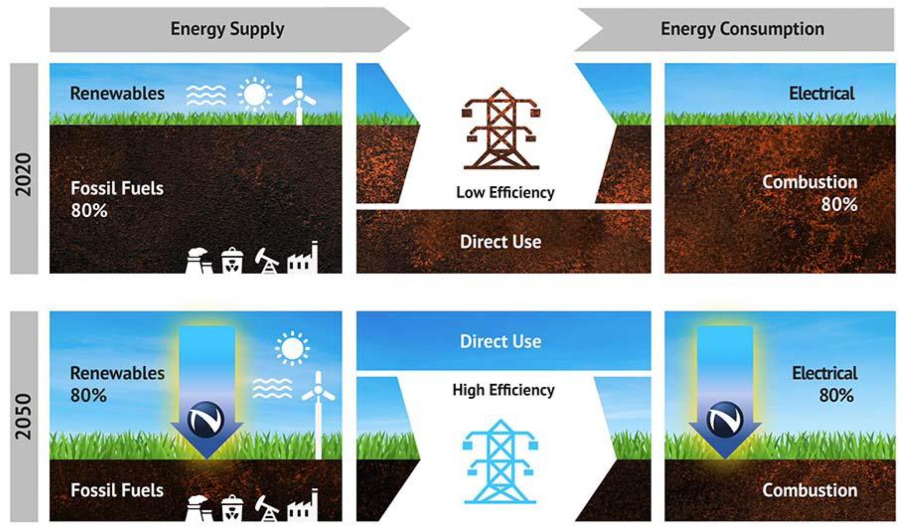
:1. Introduction
2. Si
2.1. Si Diode
2.2. Si MOSFET
2.3. Si SuperJunction MOSFET
2.4. Si IGBT
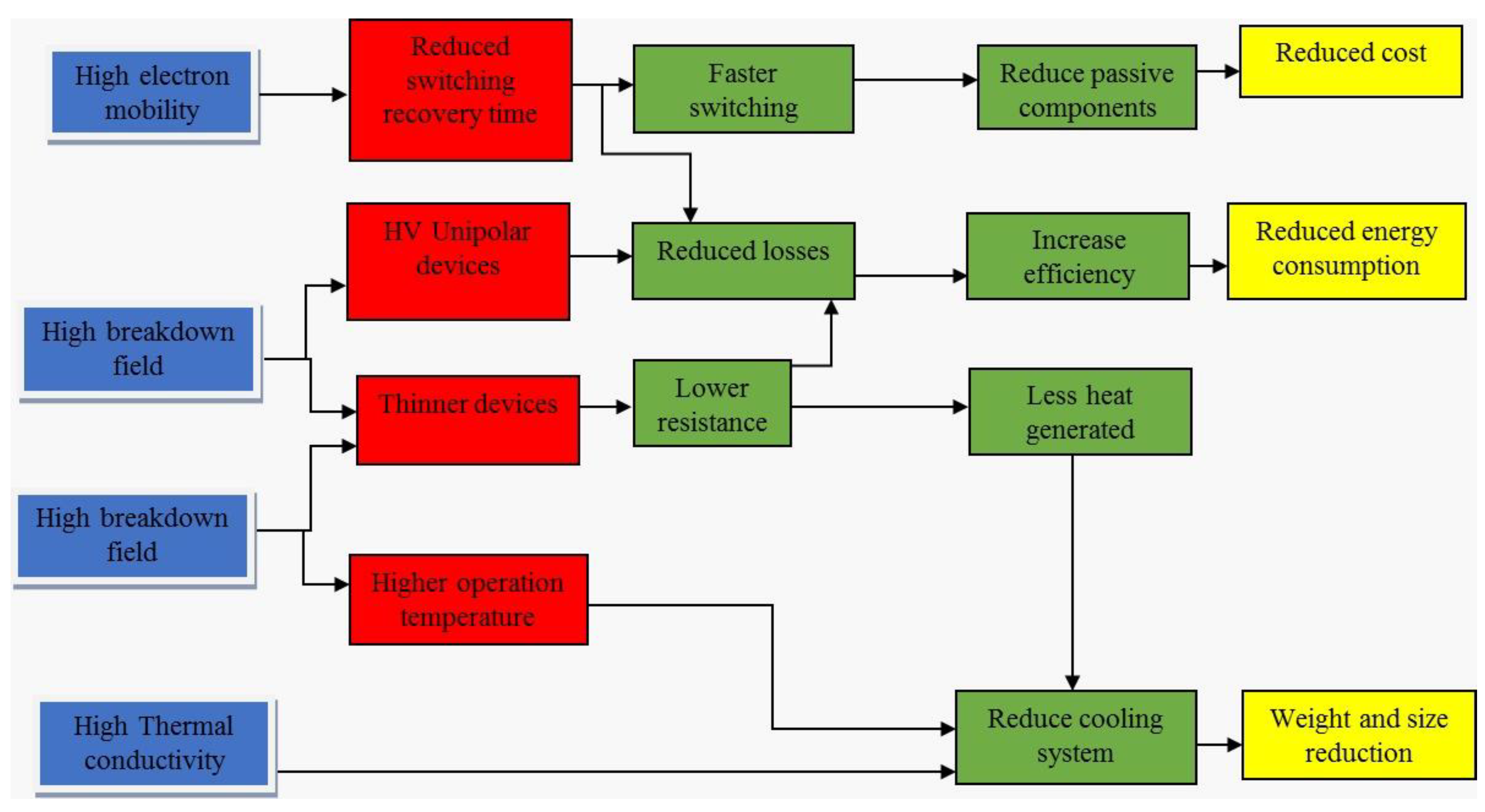
3. Silicon Carbide (SiC)
3.1. Discovery of SiC
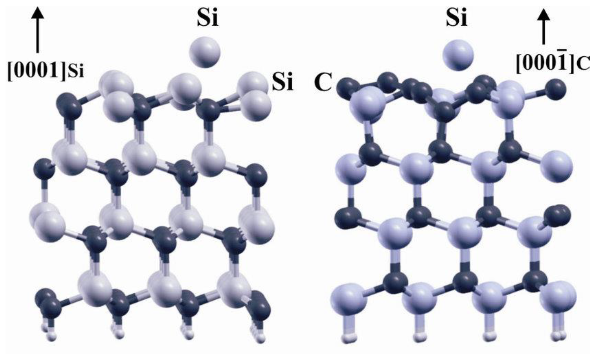
3.2. Material Growth
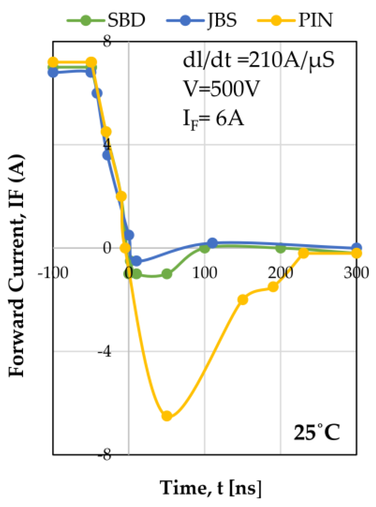
3.3. SiC Diode
3.4. SiC MOSFET
3.5. SiC IGBT
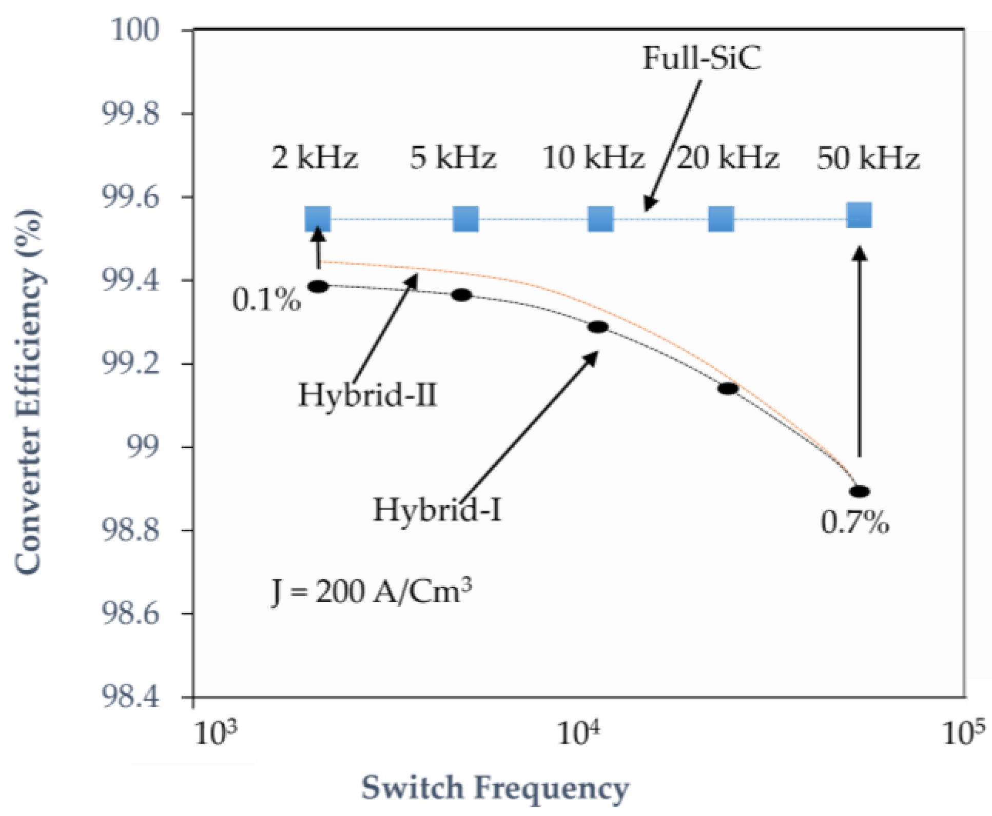
3.6. Applications and Emergence of SiC Power Electronics
3.7. Challenges of SiC Power Device Development
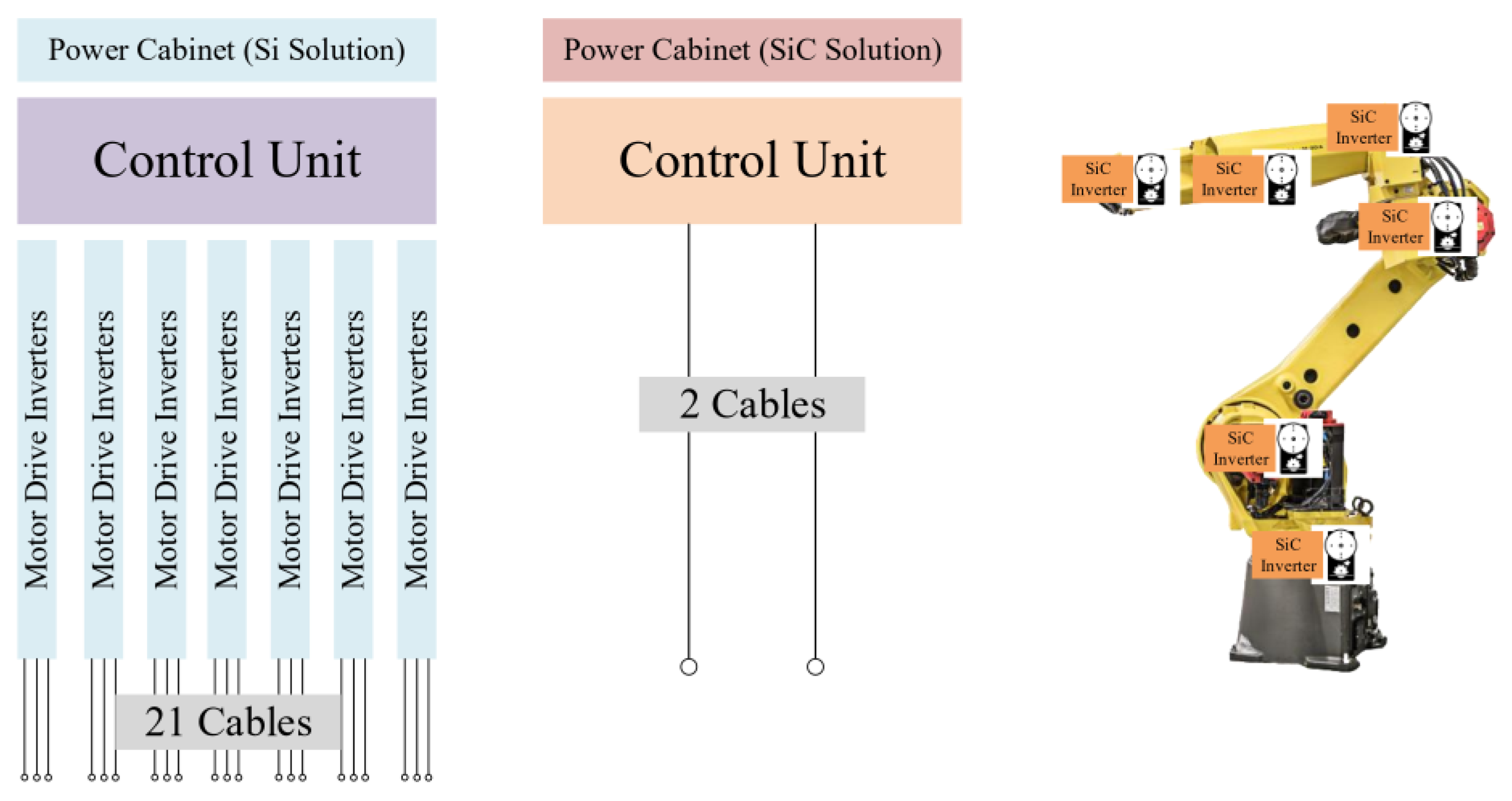
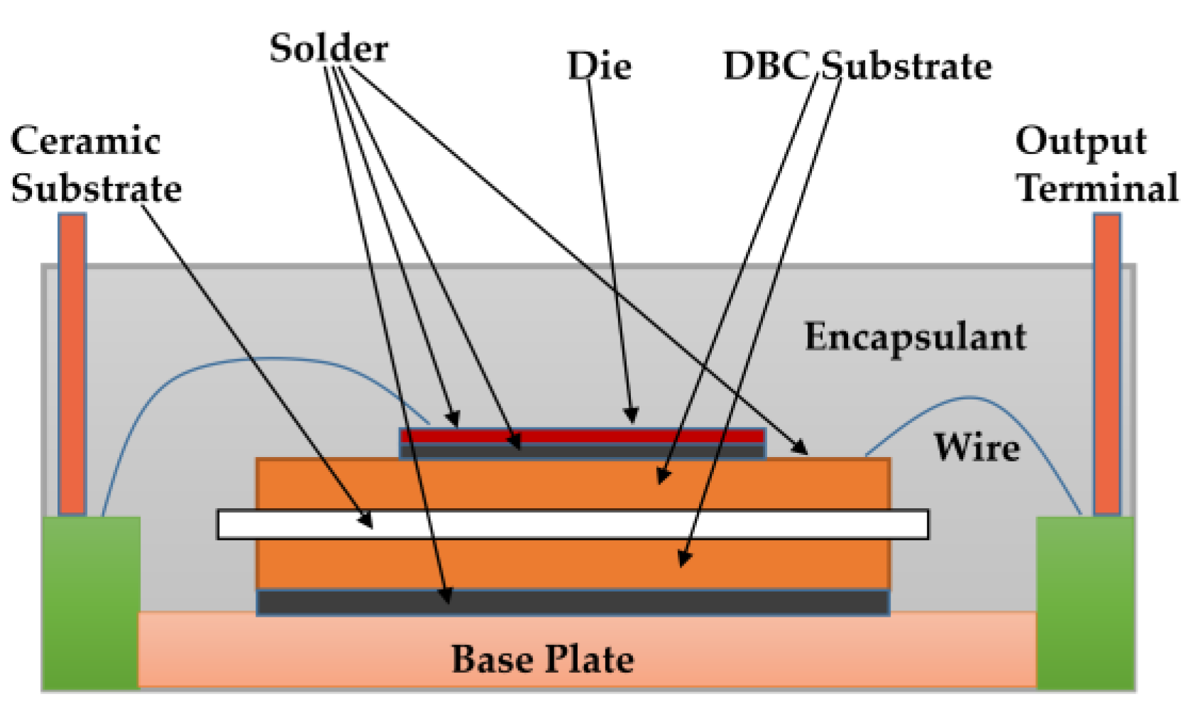
3.7.1. Packaging
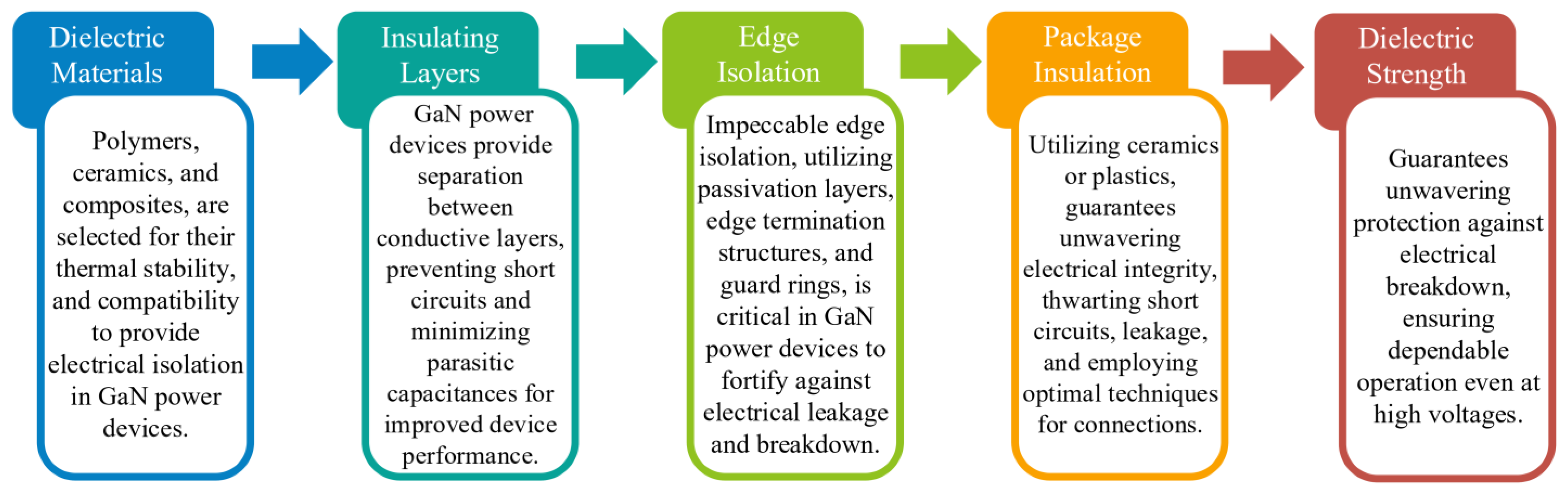
3.7.2. Electrical Insulation
3.7.3. Parasitics
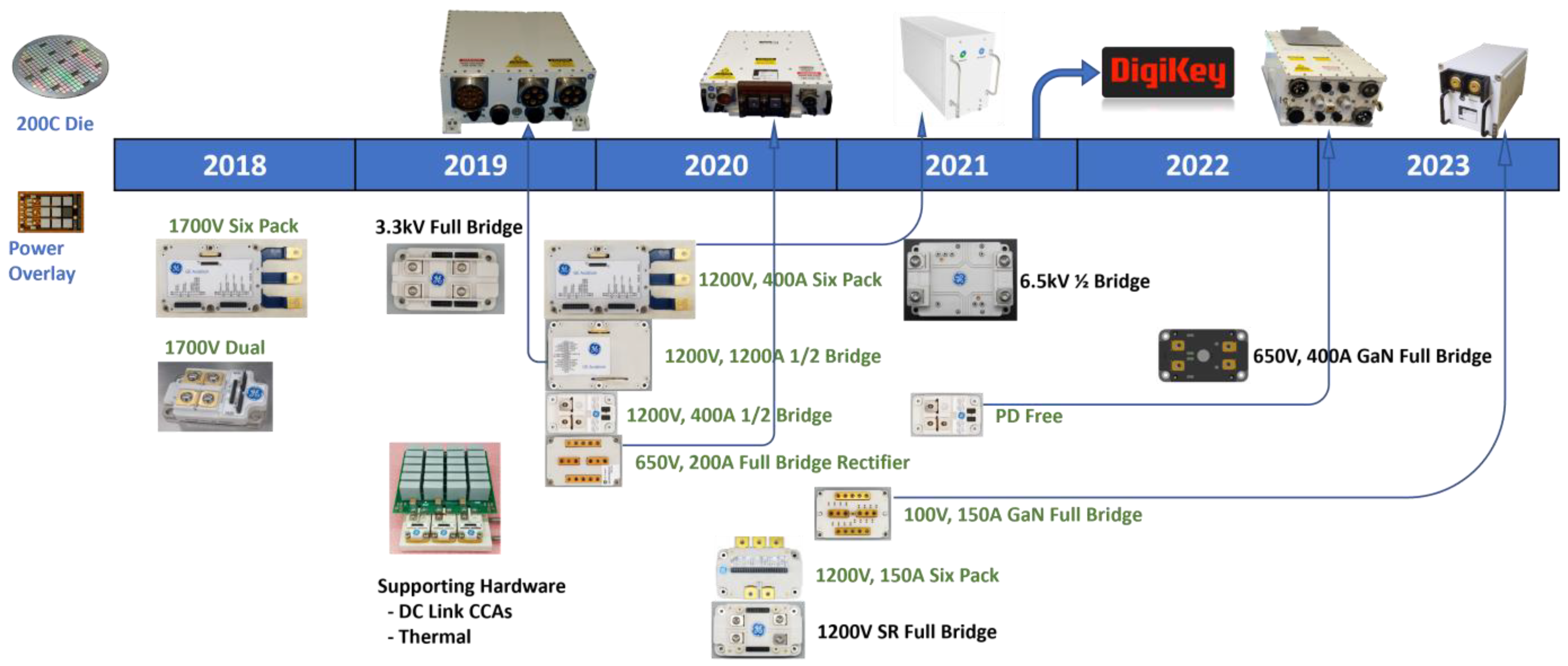
3.7.4. Power Module with Multi-Dies
3.7.5. Gate Drive
3.7.6. Electromagnetic Interference
3.8. Future Trends of SiC
3.8.1. Voltage-Derating Guidelines
3.8.2. Improving Manufacturing Techniques for Affordability
3.8.3. Considerations for SiC Device Gate Driver Design
3.8.4. Novel EMI Filter Design
3.8.5. Reducing Commutation Loop for Enhanced SiC Device Performance
3.8.6. Exploring Cooling Techniques for SiC Device Reliability
3.8.7. Advancements in Ancillary Components for High Temperature
3.8.8. Lowering Engineering Effort and Costs
4. GaN
4.1. GaN Diode
4.2. GaN MOSFET
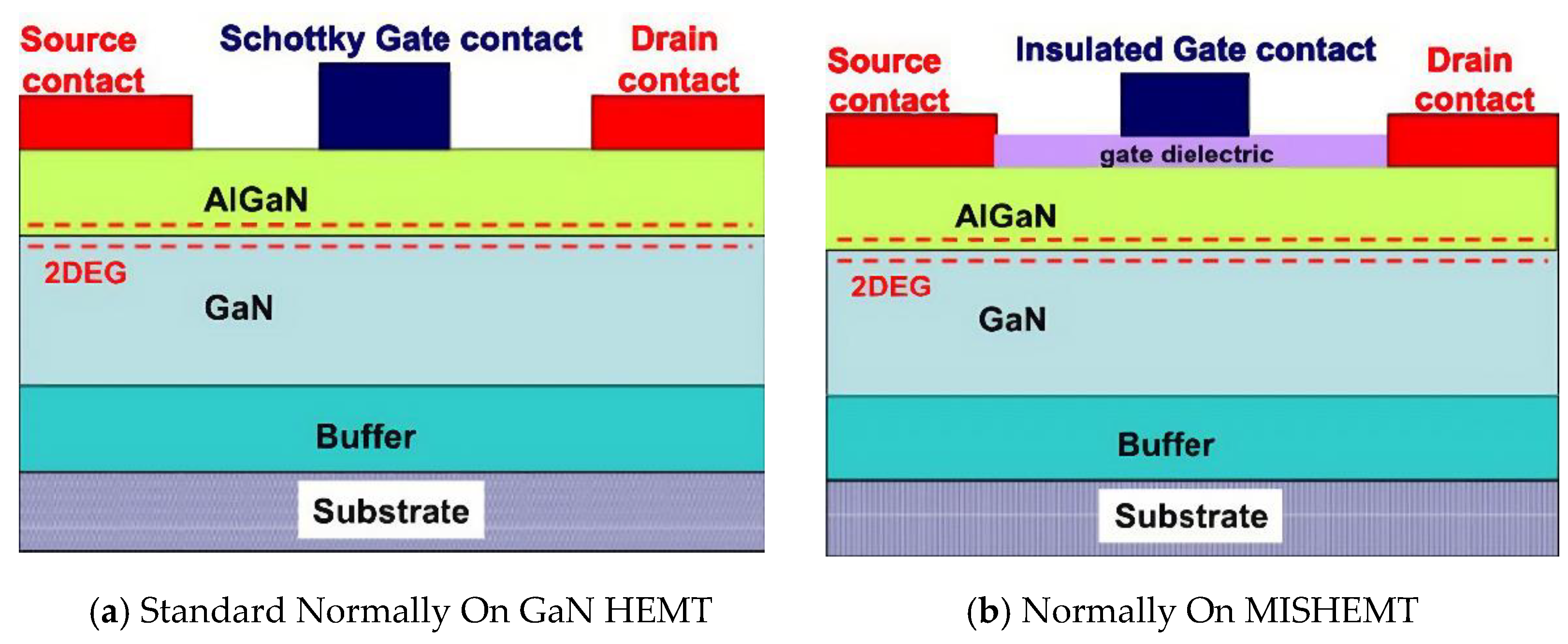
4.3. GaN Heterojunction Field-Effect Transistor (HEFT)
4.4. GaN High Electron Mobility Transistor (HEMT)
4.4.1. Enhanced GaN HEMT
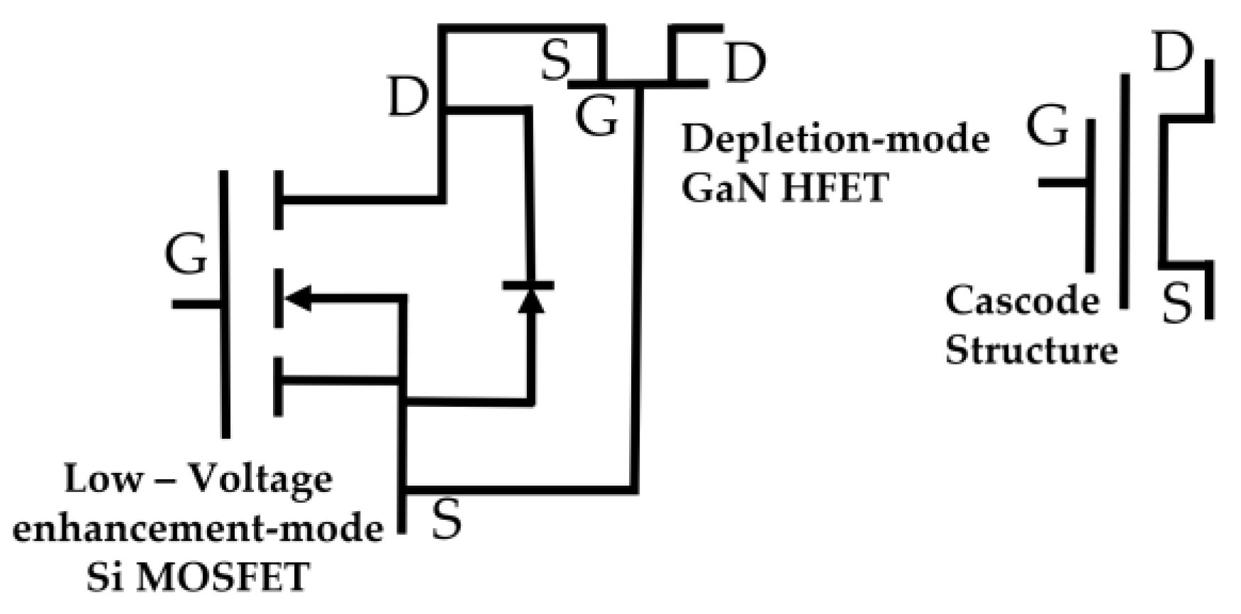
4.4.2. High-Voltage Cascade GaN HEMT
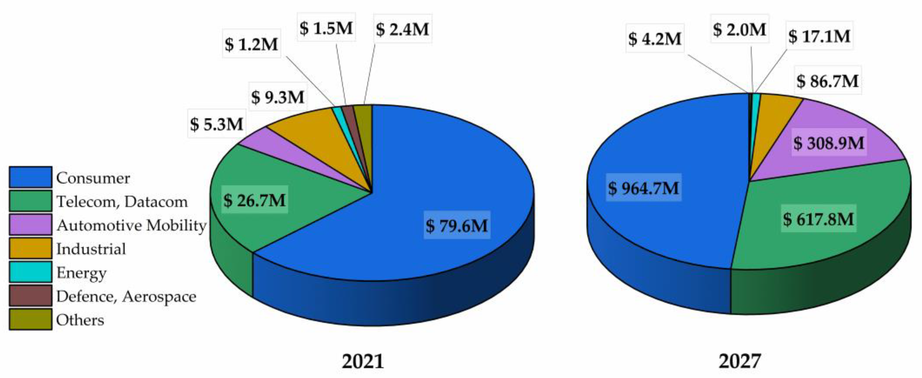
4.5. Applications of GaN
4.6. Challenges of GaN Power Device
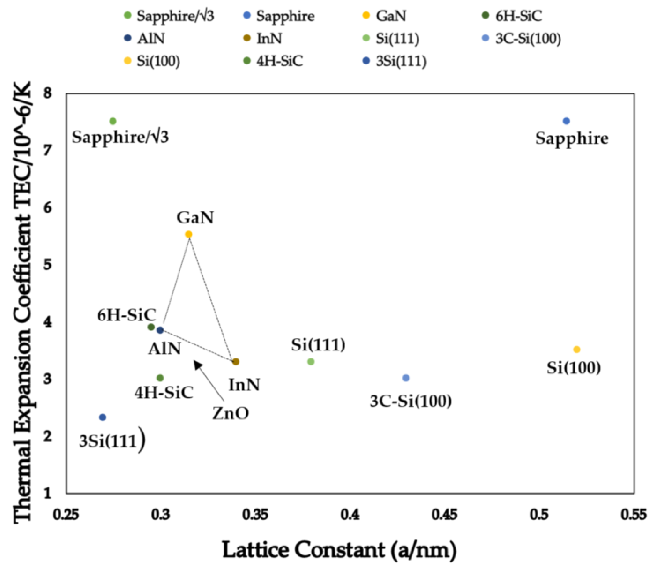
4.6.1. Material Growth
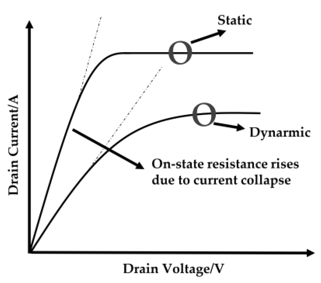
4.6.2. Suppression of Current Collapse Effect
- The current collapse is triggered by carrier traps caused by deep-level centers in the material.
- The 2DEG concentration in the AlGaN/GaN conductive channel decreases due to the change in polarization charge generated by the surface state and the surface effect, resulting in current collapse.
4.6.3. Packaging
4.6.4. Gate Driver
- Voltage and Current Levels: GaN power devices typically necessitate higher gate voltage levels in comparison to conventional Si-based devices. Operating with gate voltages ranging from 6 V to 10 V or even higher, the gate drive circuitry must be capable of generating and sustaining these elevated voltage levels. GaN power devices exhibit low gate capacitance, enabling faster switching but demanding careful attention to the gate driver’s current capability.
- Gate Driver ICs: GaN power devices often employ specialized gate driver integrated circuits (ICs). These ICs are specifically designed to deliver the required voltage and current levels, incorporate protection features, and enhance the overall performance of GaN transistors. Protection features may include under-voltage lockout (UVLO), over-current protection, and short-circuit protection to ensure device safety during operation.
- High-Speed Switching: GaN power devices are renowned for their rapid switching speeds, which can present challenges in gate drive design. To achieve optimal performance, the gate drive circuitry must be capable of providing high-speed rise and fall times to minimize switching losses. This necessitates meticulous consideration of the gate driver’s output impedance, gate trace layout, and the impact of parasitic elements in the gate circuit.
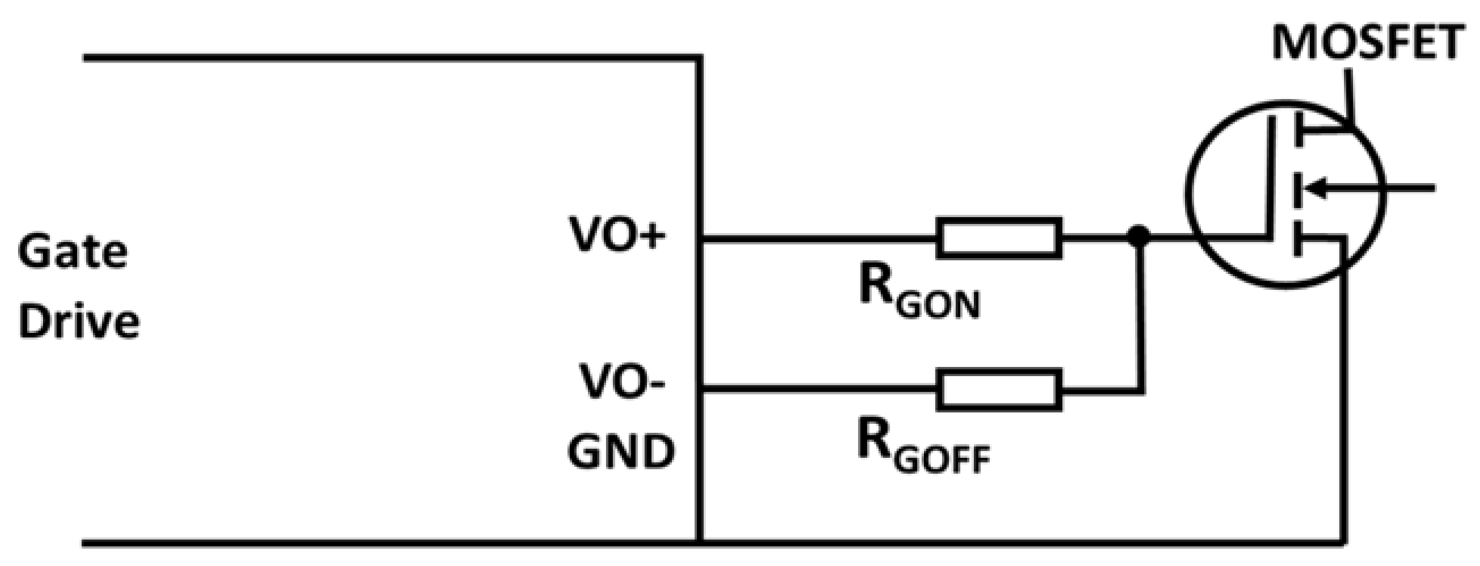
- Gate Resistance: The appropriate selection of gate resistance is crucial for GaN power devices. A suitable gate resistor aids in dampening ringing effects and mitigating the risk of oscillations in the gate voltage waveform. It also limits current during switching transitions to prevent excessive power dissipation. The value of the gate resistor should be carefully optimized based on the specific GaN device and application requirements.
- Gate Layout and Layout Considerations: A well-designed gate layout is essential in order to minimize parasitic inductances and capacitances that can negatively impact device performance. This entails keeping gate traces as short as possible, reducing loop areas, and employing techniques like guard rings and vias to manage parasitic effects. An optimized gate layout contributes to faster switching speeds, lower losses, and overall improvement in device performance.
4.6.5. Electrical Insulation
4.6.6. Electromagnetic Interference
- EMI Sources: Fast switching transitions caused by GaN power devices result in high-frequency harmonics and transient currents. These may produce electromagnetic emissions that spread through the design of the device, the circuit traces, and the connections to the outside world. During switching events, voltage peaks, ringing, and current loops are the main EMI causes in GaN power devices.
- EMI Mitigation Techniques: Several techniques are employed to mitigate EMI in GaN power devices. These include:
- Filtering: The use of passive components such as capacitors, inductors, and ferrite beads to suppress high-frequency noise and attenuate unwanted harmonics.
- Shielding: Incorporating shields, conductive enclosures, or grounded metal layers around sensitive components to contain electromagnetic fields and prevent their propagation.
- Layout Optimization: Carefully consider trace routing, component placement, and grounding techniques to minimize loop areas, reduce parasitic inductance, and control impedance.
- Grounding and Bonding: Establishing proper grounding and bonding practices to minimize ground loops, reduce voltage differentials, and provide an effective return path for high-frequency currents.
- Compliance with EMI Standards: GaN power devices must adhere to particular electromagnetic compatibility (EMC) requirements to ensure their functioning is below acceptable EMI limits. Evaluations of radiated emissions conducted emissions, and vulnerability to outside electromagnetic fields are all part of compliance testing.
- EMI Filtering Components: Choosing the right EMI filtering components is essential when creating GaN power devices. These parts must be tuned for the device’s working frequency range, have high-frequency filtering capabilities and low parasitic elements, and be parasite-free.
- EMI Simulation and Modeling: EMI behavior in GaN power devices may be predicted and examined using simulation and modeling techniques throughout the design process. Using these technologies, engineers may reduce EMI problems by optimizing circuit design, filtering tactics, and grounding procedures.
4.7. Future Trend of GaN
4.7.1. Cost Reduction
4.7.2. Thermal Management
4.7.3. Gate Driver Design
4.7.4. Motor Drive
4.7.5. 5G
4.7.6. Data Centers
5. Ultrawide Bandgap Semiconductor
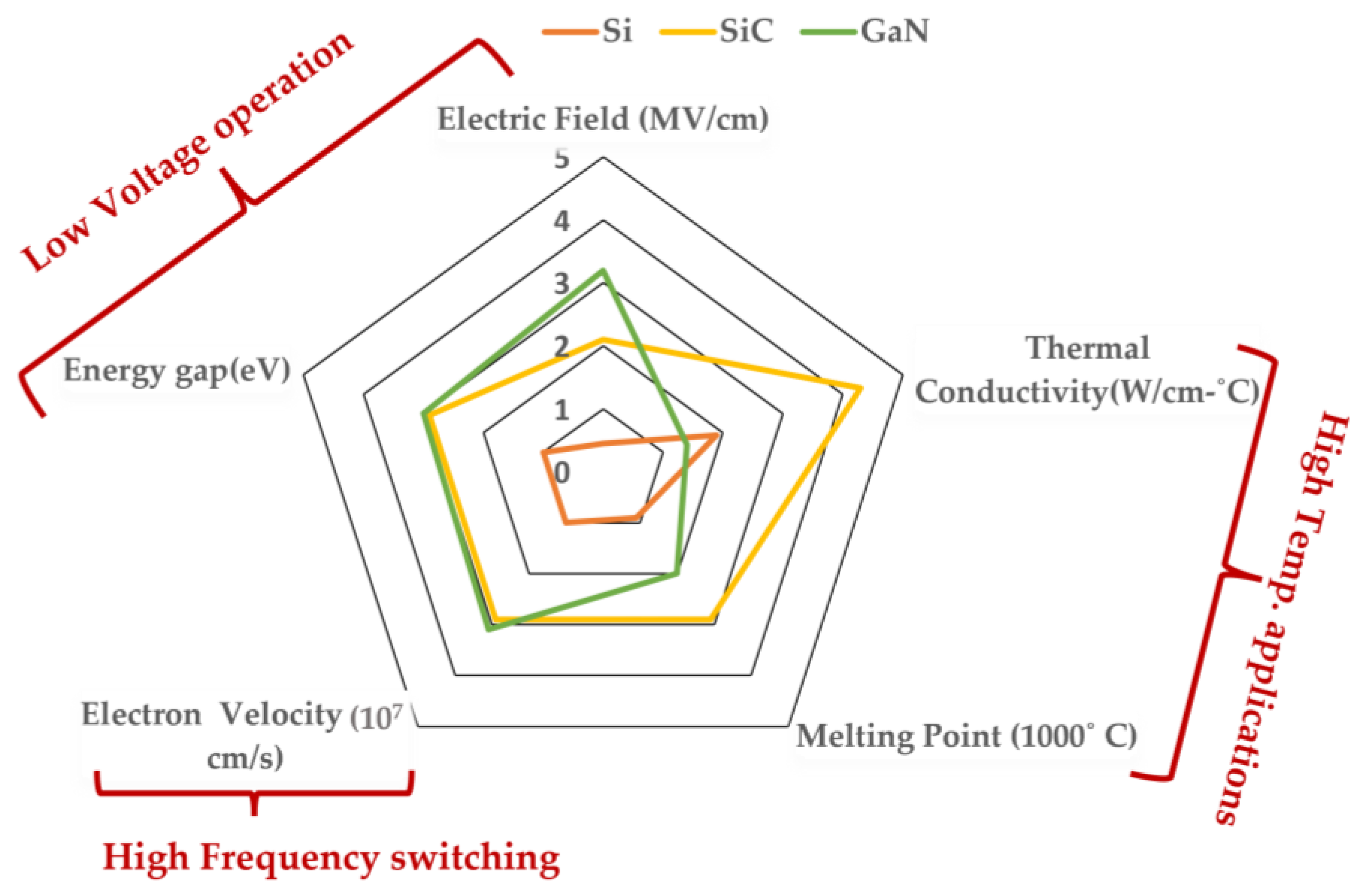
6. Current Innovation and Comparison
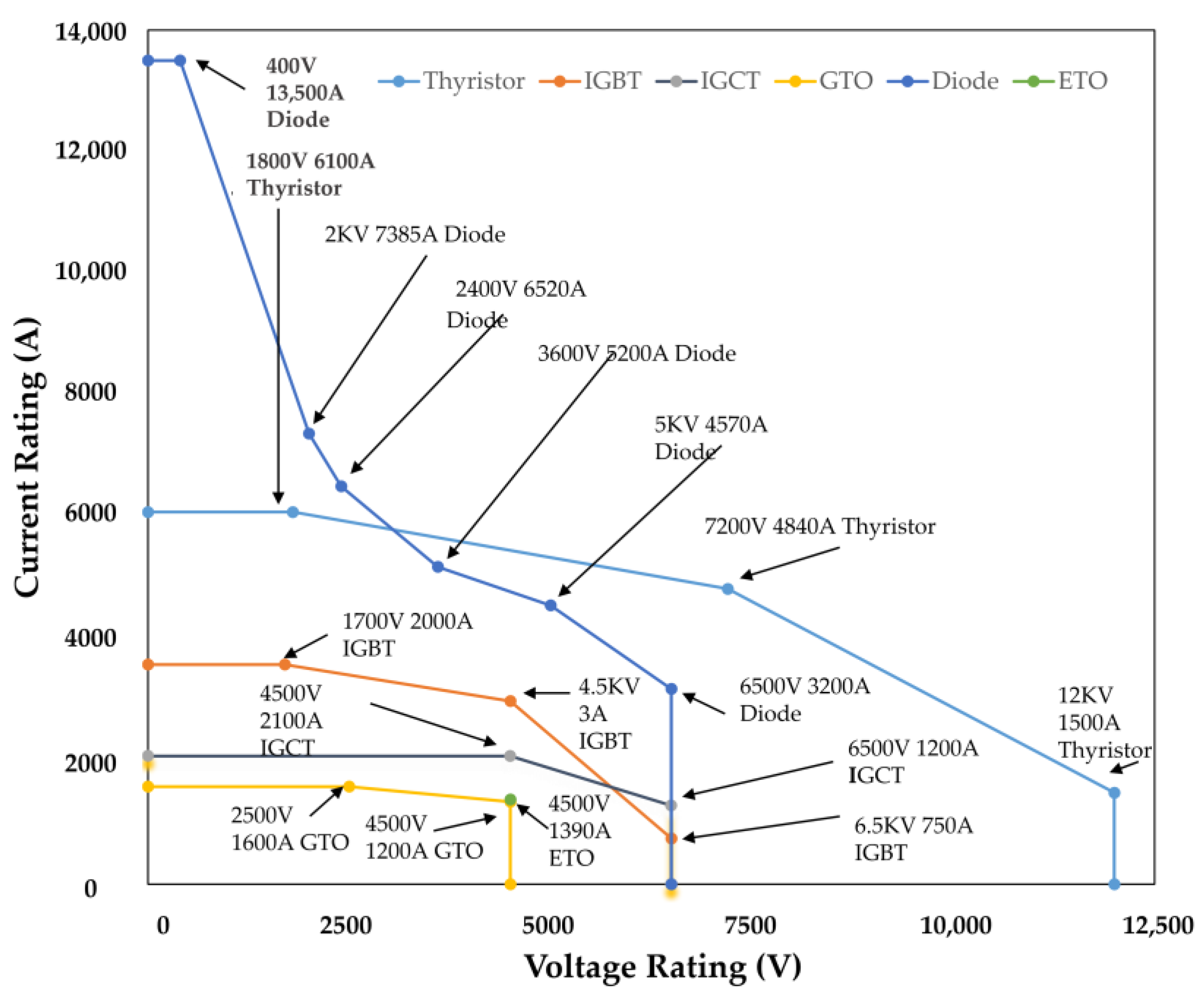
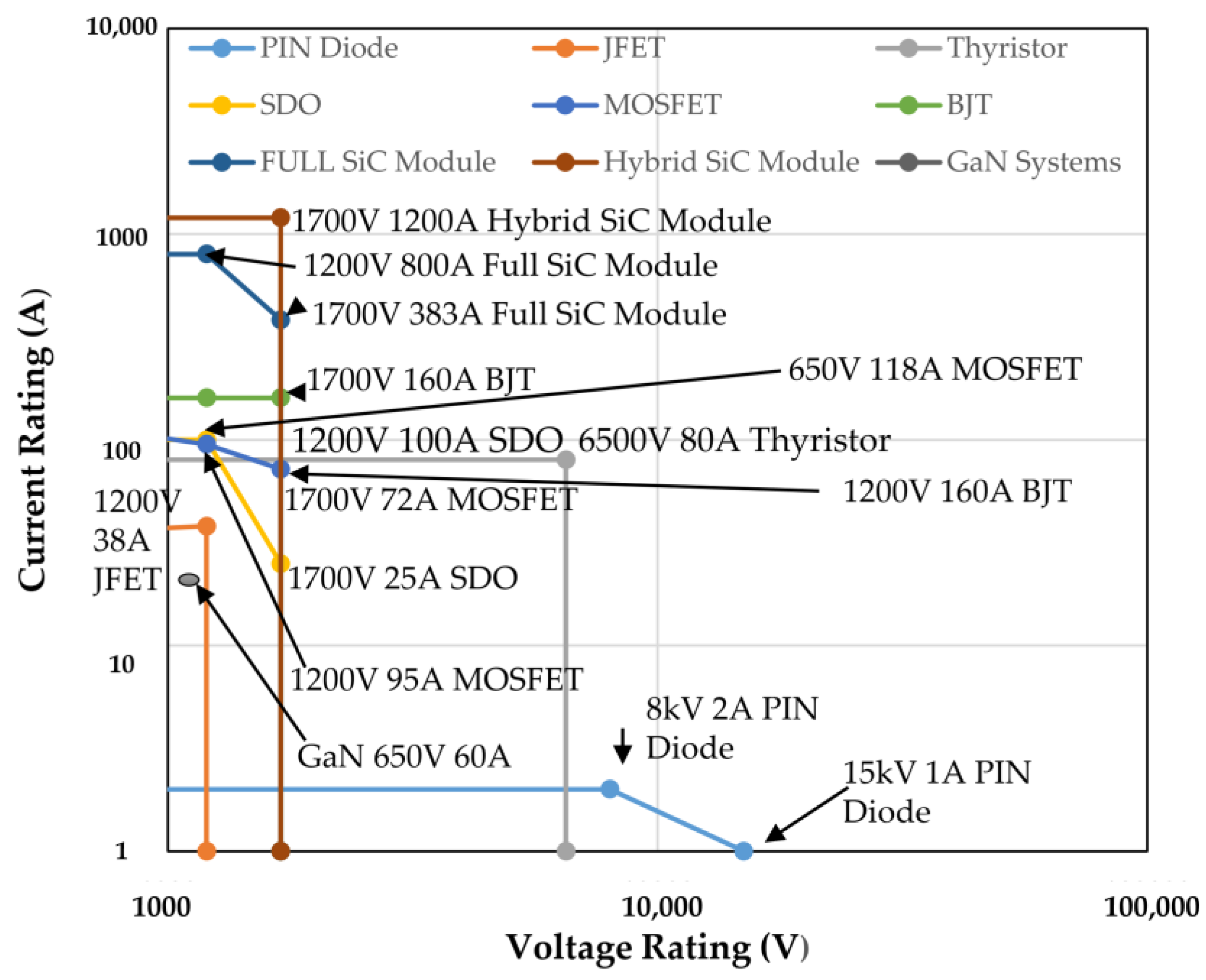
6.1. Voltage Rating
6.2. Current Rating
6.3. Switching Frequency
6.4. Thin Wafer Field Stop IGBT (FS-IGBT)
6.5. Reverse Conducting IGBT (RC-IGBT)
6.6. Reverse Blocking IGBT
6.7. Integrated Gate Commutated Thyristor (IGCT)
6.8. Reliability and Application
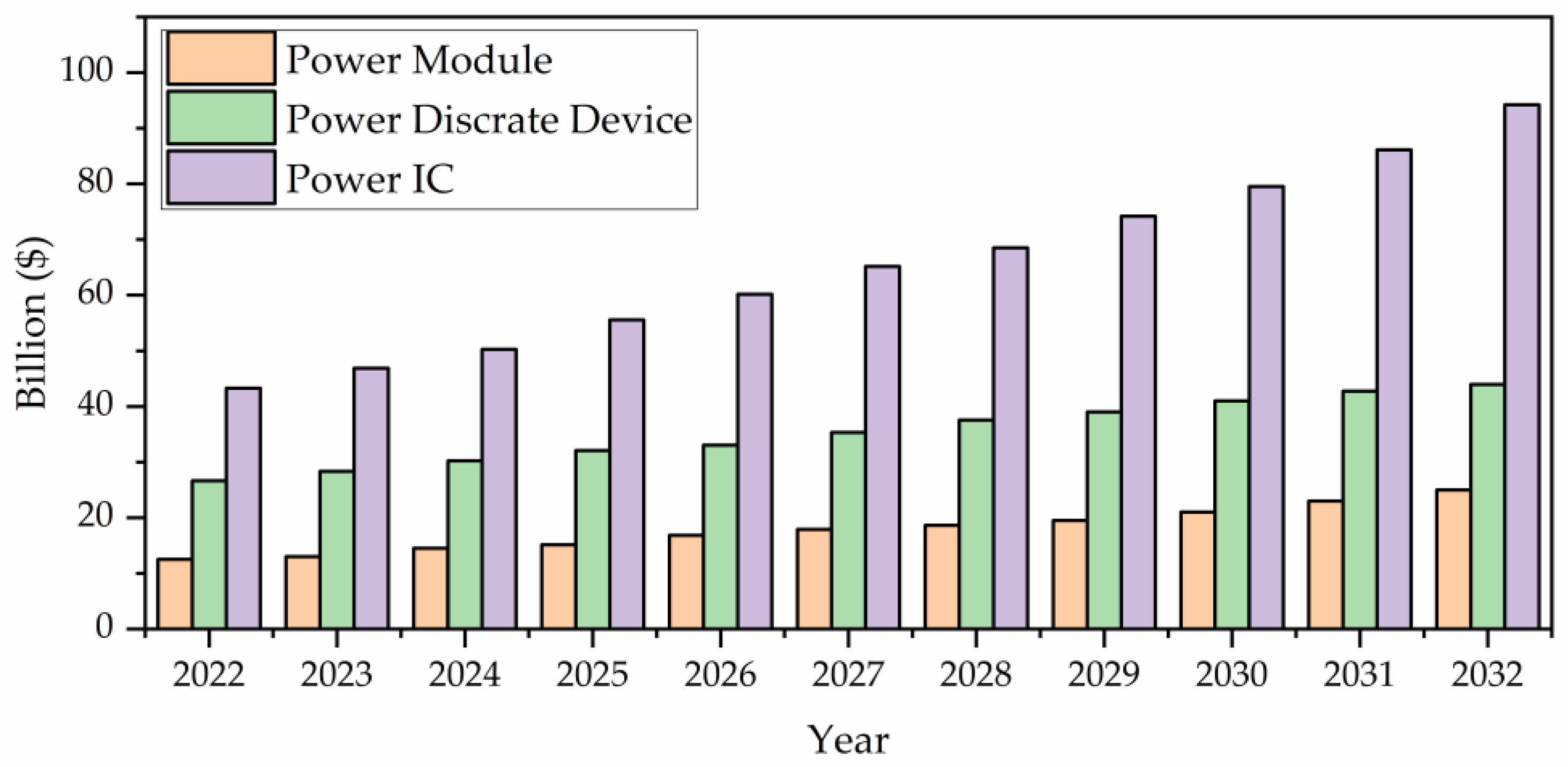
6.9. Current Marketplace Scenario
7. Conclusions
Author Contributions
Funding
Data Availability Statement
Conflicts of Interest
References
- Rafin, S.M.S.H.; Ahmed, R.; Mohammed, O.A. Wide Band Gap Semiconductor Devices for Power Electronic Converters. In Proceedings of the 2023 Fourth International Symposium on 3D Power Electronics Integration and Manufacturing (3D-PEIM), Miami, FL, USA, 1–3 February 2023; pp. 1–8. [Google Scholar]
- Palmour, J.W. SiC power device development for industrial markets. In Proceeding of the IEEE International Electron Devices Meeting (IEDM) 2014, San Francisco, CA, USA, 15–17 December 2014; pp. 1.1.1–1.1.8. [Google Scholar]
- Chow, T.P. Progress in high voltage SiC and GaN power switching devices. Mater. Sci. Forum 2014, 778-780, 1077–1082. [Google Scholar] [CrossRef]
- Rafin, S.M.S.H.; Islam, R.; Mohammed, O.A. Power Electronic Converters for Wind Power Generation. In Proceedings of the 2023 Fourth International Symposium on 3D Power Electronics Integration and Manufacturing (3D-PEIM), Miami, FL, USA, 1–3 February 2023; pp. 1–8. [Google Scholar]
- Rafin, S.M.S.H.; Haque, M.A.; Islam, R.; Mohammed, O.A. A Review of Power Electronic Converters for Electric Aircrafts. In Proceedings of the 2023 Fourth International Symposium on 3D Power Electronics Integration and Manufacturing (3D-PEIM), Miami, FL, USA, 1–3 February 2023; pp. 1–8. [Google Scholar]
- Zerarka, M.; Austin, P.; Toulon, G.; Morancho, F.; Arbess, H.; Tasselli, J. Behavioral study of single-event burnout in power devices for natural radiation environment applications. IEEE Trans. Electron Devices 2012, 59, 3482–3488. [Google Scholar] [CrossRef]
- Yu, C.-H.; Wang, Y.; Liu, J.; Sun, L.-L.J.I.T.o.E.D. Research of single-event burnout in floating field ring termination of power MOSFETs. IEEE Trans. Electron. Devices 2017, 64, 2906–2911. [Google Scholar] [CrossRef]
- Carr, J.A.; Hotz, D.; Balda, J.C.; Mantooth, H.A.; Ong, A.; Agarwal, A. Assessing the impact of SiC MOSFETs on converter interfaces for distributed energy resources. IEEE Trans. Power Electron. 2009, 24, 260–270. [Google Scholar] [CrossRef]
- Alam, M.; Kumar, K.; Dutta, V. Comparative efficiency analysis for Si, SiC MOSFETs and IGBT device for DC–DC boost converter. SN Appl. Sci. 2019, 1, 1700. [Google Scholar] [CrossRef]
- Biela, J.; Schweizer, M.; Waffler, S.; Kolar, J.W. SiC versus Si—Evaluation of potentials for performance improvement of inverter and DC–DC converter systems by SiC power semiconductors. IEEE Trans. Ind. Electron. 2010, 58, 2872–2882. [Google Scholar] [CrossRef]
- Chow, T.P. SiC and GaN high-voltage power switching devices. Mater. Sci. Forum 2000, 338–342, 1155–1160. [Google Scholar] [CrossRef]
- Guo, Y.-B.; Bhat, K.P.; Aravamudhan, A.; Hopkins, D.C.; Hazelmyer, D.R. High current and thermal transient design of a SiC SSPC for aircraft application. In Proceedings of the 2011 Twenty-Sixth Annual IEEE Applied Power Electronics Conference and Exposition (APEC), Fort Worth, TX, USA, 6–11 March 2011; pp. 1290–1297. [Google Scholar]
- Nakamura, T.; Sasagawa, M.; Nakano, Y.; Otsuka, T.; Miura, M. Large current SiC power devices for automobile applications. In Proceedings of the 2010 International Power Electronics Conference-ECCE ASIA-, Sapporo, Japan, 21–24 June 2010; pp. 1023–1026. [Google Scholar]
- Ranjbar, A. Applications of Wide Bandgap (WBG) Devices in the Transportation Sector. Recent Advances in (WBG) Semiconductor Material (e.g. SiC and GaN) and Circuit Topologies. In Transportation Electrification: Breakthroughs in Electrified Vehicles, Aircraft, Rolling Stock, and Watercraft; IEEE: Piscataway, NJ, USA, 2022; pp. 47–72. [Google Scholar]
- Roccaforte, F.; Fiorenza, P.; Greco, G.; Nigro, R.L.; Giannazzo, F.; Iucolano, F.; Saggio, M.J. Emerging trends in wide band gap semiconductors (SiC and GaN) technology for power devices. Microelectron. Eng. 2018, 187, 66–77. [Google Scholar] [CrossRef]
- Chen, K.J.; Häberlen, O.; Lidow, A.; lin Tsai, C.; Ueda, T.; Uemoto, Y.; Wu, Y. GaN-on-Si power technology: Devices and applications. IEEE Trans. Electron Devices 2017, 64, 779–795. [Google Scholar] [CrossRef]
- Tsao, J.; Chowdhury, S.; Hollis, M.; Jena, D.; Johnson, N.; Jones, K.; Kaplar, R.; Rajan, S.; Van de Walle, C.; Bellotti, E. Ultrawide-bandgap semiconductors: Research opportunities and challenges. Adv. Electron. Mater. 2018, 4, 1600501. [Google Scholar] [CrossRef]
- Al Mamun, M.; Paudyal, S.; Kamalasadan, S. Efficient Dynamic Simulation of Unbalanced Distribution Grids with Distributed Generators. In Proceedings of the 2023 IEEE Industry Applications Society Annual Meeting, Nashville, TN, USA, 29 October–2 November 2023; pp. 1–6. [Google Scholar]
- National Institute of Standards and Technology (NIST). Available online: https://www.nist.gov/pml/owm/metric-si/understanding-metric (accessed on 29 September 2023).
- Zulehner, W. Historical overview of Si crystal pulling development. Mater. Sci. Eng. 2000, 73, 7–15. [Google Scholar] [CrossRef]
- Zaidi, B. Introductory chapter: Introduction to photovoltaic effect. Sol. Panels Photovolt. Mater. 2018, 1–8. [Google Scholar] [CrossRef]
- Zaidi, B.; Hadjoudja, B.; Felfli, H.; Chouial, B.; Chibani, A. Effet des traitements thermiques sur le comportement électrique des couches de silicium polycristallin pour des applications photovoltaïques. Rev. De Métallurgie 2011, 108, 443–446. [Google Scholar] [CrossRef]
- Goetzberger, A.; Knobloch, J.; Voss, B. Crystalline Si Solar Cells; Wiley Online Library: Hoboken, NJ, USA, 1998; Volume 1. [Google Scholar]
- Zaidi, B.; Hadjoudja, B.; Felfli, H.; Chibani, A. Influence of doping and heat treatments on carriers mobility in polycrystalline Si thin films for photovoltaic application. Turk. J. Phys. 2011, 35, 185–188. [Google Scholar]
- Mathieu, H.; Bretagnon, T.; Lefebvre, P. Physique des Semiconducteurs et des Composants Electroniques-Problèmes Résolus; Dunod: Malakoff, France, 2001. [Google Scholar]
- Zaidi, B.; Saouane, I.; Shekhar, C. Electrical energy generated by amorphous Si solar panels. Si 2018, 10, 975–979. [Google Scholar]
- Zaidi, B.; Saouane, I.; Shekhar, C. Simulation of single-diode equivalent model of polycrystalline Si solar cells. Int. J. Mater. Sci. Appl. 2018, 7. [Google Scholar] [CrossRef]
- Conibeer, G. Third-generation photovoltaics. Mater. Today 2007, 10, 42–50. [Google Scholar] [CrossRef]
- Zaidi, B.; Belghit, S.; Shekhar, C.; Mekhalfa, M.; Hadjoudja, B.; Chouial, B. Electrical performance of CuInSe2 solar panels using ant colony optimization algorithm. J. Nano-Electron. Phys. 2018, 10, 05045. [Google Scholar] [CrossRef]
- Sigfússon, T.I.; Helgason, Ö. Rates of transformations in the ferroSi system. Hyperfine Interact. 1990, 54, 861–867. [Google Scholar] [CrossRef]
- Waanders, F.; Mans, A. Characterisation of ferroSi dense medium separation material. Hyperfine Interact. 2003, 148, 325–329. [Google Scholar] [CrossRef]
- Borysiuk, J.; Sołtys, J.; Bożek, R.; Piechota, J.; Krukowski, S.; Strupiński, W.; Baranowski, J.M.; Stępniewski, R. Role of structure of C-terminated 4 H-SiC (000 1−) surface in growth of graphene layers: Transmission electron microscopy and density functional theory studies. Phys. Rev. B 2012, 85, 045426. [Google Scholar] [CrossRef]
- Alsema, E.A.; de Wild-Scholten, M.J. Environmental impacts of crystalline Si photovoltaic module production. Mater. Res. Soc. Symp. Proc. 2006, 73. [Google Scholar] [CrossRef]
- Baliga, B.J. Power Semiconductor Devices. Brooks/Cole. 1995. Available online: https://www.abebooks.com/servlet/BookDetailsPL?bi=31307574601 (accessed on 29 September 2023).
- Ultra- and Hyper-Fast Si Diodes: 650V Rapid 1 and Rapid 2. Available online: https://www.infineon.com/cms/en/product/power/diodes-thyristors/Si-diodes/650v-rapid-1-and-rapid-2/ (accessed on 29 September 2023).
- Infenion. Available online: https://www.infineon.com/cms/en/product/power/diodes-thyristors/Si-diodes/600v-1200v-ultra-soft/ (accessed on 29 September 2023).
- Moller, H. Semiconductors for Solar Cells; Artech House Inc.: Norwood, MA, USA, 1993. [Google Scholar]
- Edgar, L.J. Method and Apparatus for Controlling Electric Currents. US Patent 1,745,175, 21 January 1930. [Google Scholar]
- Kahng, D. Si-Si dioxide field field induced surface devices. In Proceedings of the IRE-AIEE Solid-State Device Research Conference, Pittsburgh, PA, USA, 1960; Available online: https://scholar.google.com/scholar_lookup?title=Silicon%E2%80%93Silicon%20Dioxide%20Field%20Induced%20Surface%20Devices&author=D.K.%20State&publication_year=1960 (accessed on 29 September 2023).
- Moore, G.E. Cramming more components onto integrated circuits. IEEE 1998, 86, 82–85. [Google Scholar] [CrossRef]
- Sze, S.M.; Ng, K.K. Physics of Semiconductor Devices; John Wiley & Sons: Hoboken, NJ, USA, 2007. [Google Scholar]
- Prado, E.O.; Bolsi, P.C.; Sartori, H.C.; Pinheiro, J.R. An overview about Si, Superjunction, SiC and GaN power MOSFET technologies in power electronics applications. Energies 2022, 15, 5244. [Google Scholar] [CrossRef]
- Deboy, G.; Marz, N.; Stengl, J.-P.; Strack, H.; Tihanyi, J.; Weber, H. A new generation of high voltage MOSFETs breaks the limit line of Si. In Proceedings of the International Electron Devices Meeting 1998. Technical Digest (Cat. No. 98CH36217), San Francisco, CA, USA, 6–9 December 1998; pp. 683–685. [Google Scholar]
- Fujihira, T.; Miyasaka, Y. Simulated superior performances of semiconductor superjunction devices. In Proceedings of the 10th International Symposium on Power Semiconductor Devices and ICs. ISPSD’98 (IEEE Cat. No. 98CH36212), Kyoto, Japan, 3–6 June 1998; pp. 423–426. [Google Scholar]
- Chen, X.B. Breakthrough to the" Si limit" of power devices. In Proceedings of the 1998 5th International Conference on Solid-State and Integrated Circuit Technology, Beijing, China, 23 October 1998; pp. 141–144. [Google Scholar]
- Appels, J.; Vaes, H. High voltage thin layer devices (RESURF devices). In Proceedings of the 1979 International Electron Devices Meeting, Washington, DC, USA, 3–5 December 1979; pp. 238–241. [Google Scholar]
- Udrea, F.; Deboy, G.; Fujihira, T. Superjunction Power Devices, History, Development, and Future Prospects. IEEE Trans. Electron Device 2017, 64, 713–727. [Google Scholar] [CrossRef]
- Baliga, B.J. Insulated Gate Bipolar Transistors (IGBTs): Theory and Design; World Scientific Publishing: Singapore, 2003. [Google Scholar]
- VolLaska, T. Progress in Si IGBT Technology – as an ongoing Competition with WBG Power Devices. In Proceeding of the 2019 IEEE International Electron Devices Meeting (IEDM), San Francisco, CA, USA, 7–11 December 2019; pp. 12.2.1–12.2.4. [Google Scholar] [CrossRef]
- Vobecký, J. Design and technology of high-power Si devices. In Proceedings of the 18th International Conference Mixed Design of Integrated Circuits and Systems—MIXDES 2011, Gliwice, Poland, 16–19 June 2011; pp. 17–22. [Google Scholar]
- Guo, X.; Xun, Q.; Li, Z.; Du, S. SiC converters and MEMS devices for high-temperature power electronics: A critical review. Micromachines 2019, 10, 406. [Google Scholar] [CrossRef]
- Tian, Y.; Zetterling, C.-M. A fully integrated Si-carbide Sigma–Delta modulator operating up to 500 °C. IEEE Trans. Electron Devices 2017, 64, 2782–2788. [Google Scholar] [CrossRef]
- Garrido-Diez, D.; Baraia, I. Review of wide bandgap materials and their impact in new power devices. In Proceedings of the 2017 IEEE International Workshop of Electronics, Control, Measurement, Signals and Their Application to Mechatronics (ECMSM), Donostia, Spain, 24–26 May 2017; pp. 1–6. [Google Scholar]
- Li, K. Wide Bandgap (SiC/GaN) Power Devices Characterization and Modeling: Application to HF Power Converters. Ph.D. Thesis, École Doctorale Sciences pour L’ingénieur (Lille), Lille, France, 2014. [Google Scholar]
- Chen, C.; Luo, F.; Kang, Y. A review of SiC power module packaging: Layout, material system and integration. CPSS Trans. Power Electron. Appl. 2017, 2, 170–186. [Google Scholar] [CrossRef]
- Chabi, S.; Kadel, K. Two-dimensional SiC: Emerging direct band gap semiconductor. Nanomaterials 2020, 10, 2226. [Google Scholar] [CrossRef]
- Susi, T.; Skákalová, V.; Mittelberger, A.; Kotrusz, P.; Hulman, M.; Pennycook, T.J.; Mangler, C.; Kotakoski, J.; Meyer, J.C. Computational insights and the observation of SiC nanograin assembly: Towards 2D SiC. Sci. Rep. 2017, 7, 4399. [Google Scholar] [CrossRef]
- Ferdous, N.; Islam, M.S.; Park, J.; Hashimoto, A. Tunable electronic properties in stanene and two dimensional Si-carbide heterobilayer: A first principles investigation. AIP Adv. 2019, 9, 025120. [Google Scholar] [CrossRef]
- Chowdhury, C.; Karmakar, S.; Datta, A. Monolayer group IV–VI monochalcogenides: Low-dimensional materials for photocatalytic water splitting. J. Phys. Chem. C 2017, 121, 7615–7624. [Google Scholar] [CrossRef]
- Berzelius, J.J. Untersuchungen über die Flussspathsäure und deren merkwürdigsten Verbindungen. Ann. Der Phys. 1824, 77, 169–230. [Google Scholar] [CrossRef]
- Pensl, G.; Ciobanu, F.; Frank, T.; Krieger, M.; Reshanov, S.; Schmid, F.; Weidner, M. Sic material properties. In Sic Materials And Devices; World Scientific: Singapore, 2006; Volume 1, pp. 1–41. [Google Scholar]
- Acheson, E.G. Carborundum: Its history, manufacture and uses. J. Frankl. Inst. 1893, 136, 279–289. [Google Scholar] [CrossRef]
- Kaminskiy, F.; Bukin, V.; Potapov, S.; Arkus, N.; Ivanova, V. Discoveries of SiC under natural conditions and their genetic importance. Int. Geol. Rev. 1969, 11, 561–569. [Google Scholar] [CrossRef]
- Choyke, W.J.; Patrick, L.; Ziegler, J. (Eds.) SiC 2: Materials, Processing, and Devices; Springer: Berlin/Heidelberg, Germany, 2018. [Google Scholar]
- Kimoto, T.; Cooper, J.A. Fundamentals of SiC Technology: Growth, Characterization, Devices and Applications; John Wiley & Sons: Hoboken, NJ, USA, 2014. [Google Scholar]
- Zhang, Y.; Suzuki, T. Epitaxial Growth of SiC—Review on Growth Mechanism and Technology. J. Cryst. Growth 2019, 512, 1–22. [Google Scholar]
- Singh, R.; Capell, D.C.; Hefner, A.R.; Lai, J.; Palmour, J.W. High-power 4H-SiC JBS rectifiers. IEEE Trans. Electron. Devices 2002, 49, 2054–2063. [Google Scholar] [CrossRef]
- Huang, X.; Wang, G.; Lee, M.-C.; Huang, A.Q. Reliability of 4H-SiC SBD/JBS diodes under repetitive surge current stress. In Proceedings of the 2012 IEEE Energy Conversion Congress and Exposition (ECCE), Raleigh, NC, USA, 15–20 September 2012; pp. 2245–2248. [Google Scholar]
- Cheung, K.P. SiC power MOSFET gate oxide breakdown reliability—Current status. In Proceedings of the 2018 IEEE International Reliability Physics Symposium (IRPS), Burlingame, CA, USA, 11–15 March 2018; pp. 2B. 3-1–2B. 3-5. [Google Scholar]
- Wang, J.; Jiang, X. Review and analysis of SiC MOSFETs’ ruggedness and reliability. IET Power Electron. 2020, 13, 445–455. [Google Scholar] [CrossRef]
- She, X.; Huang, A.Q.; Lucia, O.; Ozpineci, B. Review of SiC power devices and their applications. IEEE Trans. Ind. Electron. 2017, 64, 8193–8205. [Google Scholar] [CrossRef]
- Guo, S.; Zhang, L.; Lei, Y.; Li, X.; Xue, F.; Yu, W.; Huang, A.Q. 3.38 Mhz operation of 1.2 kV SiC MOSFET with integrated ultra-fast gate drive. In Proceedings of the 2015 IEEE 3rd Workshop on Wide Bandgap Power Devices and Applications (WiPDA), Blacksburg, VA, USA, 2–4 November 2015; pp. 390–395. [Google Scholar]
- Pérez-Tomás, A.; Brosselard, P.; Hassan, J.; Jorda, X.; Godignon, P.; Placidi, M.; Constant, A.; Millán, J.; Bergman, J. Schottky versus bipolar 3.3 kV SiC diodes. Semicond. Sci. Technol. 2008, 23, 125004. [Google Scholar] [CrossRef]
- Langpoklakpam, C.; Liu, A.-C.; Chu, K.-H.; Hsu, L.-H.; Lee, W.-C.; Chen, S.-C.; Sun, C.-W.; Shih, M.-H.; Lee, K.-Y.; Kuo, H.-C. Review of SiC processing for power MOSFET. Crystals 2022, 12, 245. [Google Scholar] [CrossRef]
- Losee, P.; Bolotnikov, A.; Yu, L.; Beaupre, R.; Stum, Z.; Kennerly, S.; Dunne, G.; Sui, Y.; Kretchmer, J.; Johnson, A. 1.2 kV class SiC MOSFETs with improved performance over wide operating temperature. In Proceedings of the 2014 IEEE 26th International Symposium on Power Semiconductor Devices & IC’s (ISPSD), Waikoloa, HI, USA, 15–149 June 2014; pp. 297–300. [Google Scholar]
- DiMarino, C.M.; Burgos, R.; Dushan, B. High-temperature SiC: Characterization of state-of-the-art SiC power transistors. IEEE Ind. Electron. Mag. 2015, 9, 19–30. [Google Scholar] [CrossRef]
- Qingwen, S.; Xiaoyan, T.; Yimeng, Z.; Yuming, Z.; Yimen, Z. Investigation of SiC trench MOSFET with floating islands. IET Power Electron. 2016, 9, 2492–2499. [Google Scholar] [CrossRef]
- Jiang, H.; Wei, J.; Dai, X.; Ke, M.; Deviny, I.; Mawby, P. SiC trench MOSFET with shielded fin-shaped gate to reduce oxide field and switching loss. IEEE Electron. Device Lett. 2016, 37, 1324–1327. [Google Scholar] [CrossRef]
- Hiyoshi, T.; Uchida, K.; Sakai, M.; Furumai, M.; Tsuno, T.; Mikamura, Y. Gate oxide reliability of 4H-SiC V-groove trench MOSFET under various stress conditions. In Proceedings of the 2016 28th international Symposium on Power Semiconductor devices and ics (iSPSd), Prague, Czech Republic, 12–16 June 2016; pp. 39–42. [Google Scholar]
- Song, Q.; Yang, S.; Tang, G.; Han, C.; Zhang, Y.; Tang, X.; Zhang, Y.; Zhang, Y. 4H-SiC trench MOSFET with L-shaped gate. IEEE Electron. Device Lett. 2016, 37, 463–466. [Google Scholar] [CrossRef]
- Wang, Y.; Tian, K.; Hao, Y.; Yu, C.-H.; Liu, Y.-J. An optimized structure of 4H-SiC U-shaped trench gate MOSFET. IEEE Trans. Electron Devices 2015, 62, 2774–2778. [Google Scholar] [CrossRef]
- Takaya, H.; Morimoto, J.; Hamada, K.; Yamamoto, T.; Sakakibara, J.; Watanabe, Y.; Soejima, N. A 4H-SiC trench MOSFET with thick bottom oxide for improving characteristics. In Proceedings of the 2013 25th International Symposium on Power Semiconductor Devices & IC’s (ISPSD), Kanazawa, Japan, 26–30 May 2013; pp. 43–46. [Google Scholar]
- Nakajima, A.; Saito, W.; Nishizawa, S.-i.; Ohashi, H. Theoretical Loss Analysis of Power Converters with 1200 V Class Si-IGBT and SiC-MOSFET. In Proceedings of the Proceedings of Pcim europe 2015; International Exhibition and Conference for Power Electronics, Intelligent Motion, Renewable Energy and Energy Management, Nuremberg, Germany, 19–20 May 2015; pp. 1–6. [Google Scholar]
- Arrow. Available online: https://www.arrow.com/en/research-and-events/articles/advantages-of-sic-mosfet-vs-si-igbt (accessed on 29 September 2023).
- Rafin, S.M.S.H.; Mohammed, O.A. Novel Dual Inverter Sub-Harmonic Synchronous Machines. IEEE Trans. Magn. 2023, 59, 8202605. [Google Scholar] [CrossRef]
- Rafin, S.M.S.H.; Ali, Q.; Mohammed, O.A. Hybrid Sub-Harmonic Synchronous Machines Using Series and Parallel Consequent Permanent Magnet. In Proceedings of the 2023 IEEE Energy Conversion Congress and Exposition (ECCE), Nashville, TN, USA, 29 October – 2 November 2023; pp. 1–5. [Google Scholar]
- Rafin, S.M.S.H.; Ali, Q.; Mohammed, O.A. Novel PM-Assisted Model of the Two-Layer Sub-Harmonic Synchronous Machines. In Proceedings of the 2023 International Applied Computational Electromagnetics Society Symposium (ACES), Monterey/Seaside, CA, USA, 26–30 March 2023; pp. 1–2. [Google Scholar]
- Rafin, S.M.S.H.; Mohammed, O.A. Sub-Harmonic Synchronous Machine Using a Dual Inverter and a Unique Three-Layer Stator Winding. In Proceedings of the 2023 IEEE International Magnetic Conference-Short Papers (INTERMAG Short Papers), Sendai, Japan, 15–19 May 2023; pp. 1–2. [Google Scholar]
- Rafin, S.M.S.H.; Ali, Q.; Lipo, T.A. A novel sub-harmonic synchronous machine using three-layer winding topology. World Electr. Veh. J. 2022, 13, 16. [Google Scholar] [CrossRef]
- Rafin, S.M.S.H.; Ali, Q.; Khan, S.; Lipo, T.A. A novel two-layer winding topology for sub-harmonic synchronous machines. Electr. Eng. 2022, 104, 3027–3035. [Google Scholar] [CrossRef]
- Kadavelugu, A.; Mainali, K.; Patel, D.; Madhusoodhanan, S.; Tripathi, A.; Hatua, K.; Bhattacharya, S.; Ryu, S.-H.; Grider, D.; Leslie, S. Medium voltage power converter design and demonstration using 15 kV SiC N-IGBTs. In Proceedings of the 2015 IEEE Applied Power Electronics Conference and Exposition (APEC), Charlotte, NC, USA, 15–19 March 2015; pp. 1396–1403. [Google Scholar]
- Rahimo, M.; Kopta, A.; Eicher, S.; Kaminski, N.; Bauer, F.; Schlapbach, U.; Linder, S. Extending the boundary limits of high voltage IGBTs and diodes to above 8 kV. In Proceedings of the 14th International Symposium on Power Semiconductor Devices and Ics, Sante Fe, NM, USA, 7 June 2002; pp. 41–44. [Google Scholar]
- Wang, G.; Huang, A.Q.; Wang, F.; Song, X.; Ni, X.; Ryu, S.-H.; Grider, D.; Schupbach, M.; Palmour, J. Static and dynamic performance characterization and comparison of 15 kV SiC MOSFET and 15 kV SiC n-IGBTs. In Proceedings of the 2015 IEEE 27th International Symposium on Power Semiconductor Devices & IC’s (ISPSD), Hong Kong, China, 10–14 May 2015; pp. 229–232. [Google Scholar]
- Abdalgader, I.A.; Kivrak, S.; Özer, T. Power performance comparison of SiC-IGBT and Si-IGBT switches in a three-phase inverter for aircraft applications. Micromachines 2022, 13, 313. [Google Scholar] [CrossRef]
- Ramungul, N.; Chow, T.; Ghezzo, M.; Kretchmer, J.; Hennessy, W. A fully planarized, 6H-SiC UMOS insulated-gate bipolar transistor. In Proceedings of the 1996 54th Annual Device Research Conference Digest, Santa Barbara, CA, USA, 26 June 1996; pp. 56–57. [Google Scholar]
- Zhang, Q.; Jonas, C.; Callanan, R.; Sumakeris, J.; Das, M.; Agarwal, A.; Palmour, J.; Ryu, S.-H.; Wang, J.; Huang, A. New Improvement Results on 7.5 kV 4H-SiC p-IGBTs with R diff, on of 26 mΩ·cm 2 at 25 °C. In Proceedings of the 19th International Symposium on Power Semiconductor Devices and IC’s, Jeju, Republic of Korea, 27–31 May 2007; pp. 281–284. [Google Scholar]
- Avram, M.; Brezeanu, G.; Avram, A.; Neagoe, O.; Brezeanu, M.; Iliescu, C.; Codreanu, C.; Voitincu, C. Contributions to development of high power SiC-IGBT. In Proceedings of the CAS 2005 Proceedings. 2005 International Semiconductor Conference, Sinaia, Romania, 3–5 October 2005; pp. 365–368. [Google Scholar]
- Wang, X.; Cooper, J.A. High-voltage n-channel IGBTs on free-standing 4H-SiC epilayers. IEEE Trans. Electron. Devices 2010, 57, 511–515. [Google Scholar] [CrossRef]
- Van Brunt, E.; Cheng, L.; O’Loughlin, M.J.; Richmond, J.; Pala, V.; Palmour, J.W.; Tipton, C.W.; Scozzie, C. 27 kV, 20 A 4H-SiC n-IGBTs. Mater. Sci. Forum 2015, 821–823, 847–850. [Google Scholar] [CrossRef]
- Madhusoodhanan, S.; Hatua, K.; Bhattacharya, S.; Leslie, S.; Ryu, S.-H.; Das, M.; Agarwal, A.; Grider, D. Comparison study of 12kV n-type SiC IGBT with 10kV SiC MOSFET and 6.5 kV Si IGBT based on 3L-NPC VSC applications. In Proceedings of the 2012 IEEE Energy Conversion Congress and Exposition (ECCE), Raleigh, NC, USA, 15–20 September 2012; pp. 310–317. [Google Scholar]
- Kadavelugu, A.; Bhattacharya, S.; Ryu, S.-H.; Van Brunt, E.; Grider, D.; Agarwal, A.; Leslie, S. Characterization of 15 kV SiC n-IGBT and its application considerations for high power converters. In Proceedings of the 2013 IEEE Energy Conversion Congress and Exposition, Denver, CO, USA, 15–19 September 2013; pp. 2528–2535. [Google Scholar]
- Tripathi, A.; Mainali, K.; Madhusoodhanan, S.; Patel, D.; Kadavelugu, A.; Hazra, S.; Bhattacharya, S.; Hatua, K. MVDC microgrids enabled by 15kV SiC IGBT based flexible three phase dual active bridge isolated DC-DC converter. In Proceedings of the 2015 IEEE Energy Conversion Congress and Exposition (ECCE), Montreal, QC, Canada, 20–24 September 2015; pp. 5708–5715. [Google Scholar]
- Han, L.; Liang, L.; Kang, Y.; Qiu, Y. A Review of SiC IGBT: Models, Fabrications, Characteristics, and Applications. IEEE Trans. Power Electron. 2021, 36, 2080–2093. [Google Scholar] [CrossRef]
- Ciuti, G.; Ricotti, L.; Menciassi, A.; Dario, P. MEMS sensor technologies for human centred applications in healthcare, physical activities, safety and environmental sensing: A review on research activities in Italy. Sensors 2015, 15, 6441–6468. [Google Scholar] [CrossRef]
- Funaki, T.; Balda, J.C.; Junghans, J.; Kashyap, A.S.; Mantooth, H.A.; Barlow, F.; Kimoto, T.; Hikihara, T. Power conversion with SiC devices at extremely high ambient temperatures. IEEE Trans. Power Electron. 2007, 22, 1321–1329. [Google Scholar] [CrossRef]
- Katoh, Y.; Snead, L.L. SiC and its composites for nuclear applications–Historical overview. J. Nucl. Mater. 2019, 526, 151849. [Google Scholar] [CrossRef]
- Ning, P.; Wang, F.; Ngo, K.D. High-temperature SiC power module electrical evaluation procedure. IEEE Trans. Power Electron. 2011, 26, 3079–3083. [Google Scholar] [CrossRef]
- Wang, R.; Boroyevich, D.; Ning, P.; Wang, Z.; Wang, F.; Mattavelli, P.; Ngo, K.D.; Rajashekara, K. A high-temperature sic three-phase ac-dc converter design for> 100/spl deg/c ambient temperature. IEEE Trans. Power Electron. 2012, 28, 555–572. [Google Scholar] [CrossRef]
- Carbosystem. Available online: https://carbosystem.com/en/Si-carbide-properties-applications (accessed on 29 September 2023).
- Zabihi, N.; Mumtaz, A.; Logan, T.; Daranagama, T.; McMahon, R.A. SiC power devices for applications in hybrid and electric vehicles. Mater. Sci. Forum 2019, 963, 869–872. [Google Scholar] [CrossRef]
- Durham, N. Cree Launches Industry’s First Commercial SiC Power Mosfet. 2011. Available online: https://compoundsemiconductor.net/article/87227/Cree_Launches_Industry%E2%80%99s_First_Commercial_SiC_Power_MOSFET (accessed on 29 September 2023).
- STMicroelectronics: STPOWER SiC MOSFETs. Available online: https://www.st.com/en/power-transistors/stpower-sic-mosfets.html (accessed on 29 September 2023).
- Cai, W.; Wu, X.; Zhou, M.; Liang, Y.; Wang, Y. Review and development of electric motor systems and electric powertrains for new energy vehicles. Automot. Innov. 2021, 4, 3–22. [Google Scholar] [CrossRef]
- Greencarcongress. Available online: https://www.greencarcongress.com/2023/04/20230404-denso.html (accessed on 29 September 2023).
- Hamdan, M. Keynote: The Development and Use of SiC Power Devices in Aerospace Applications. In Proceedings of the IEEE Design Methodologies Conference 2023, Miami, FL, USA, 24-26 September 2023. [Google Scholar]
- 200kW Integrated Starter Generator Controller. Available online: https://www.geaerospace.com/sites/default/files/2022-03/200kW-Integrated-Starter-Generator-Controller%20%281%29.pdf (accessed on 29 September 2023).
- SiC Power Modules. Available online: https://www.geaerospace.com/sites/default/files/Si-Carbide-Power-Modules-2020.12.pdf (accessed on 29 September 2023).
- Rafin, S.M.S.H.; Lipo, T.A.; Kwon, B.-I. Performance analysis of the three transistor voltage source inverter using different PWM techniques. In Proceedings of the 2015 9th International Conference on Power Electronics and ECCE Asia (ICPE-ECCE Asia), Seoul, Republic of Korea, 1–5 June 2015; pp. 1428–1443. [Google Scholar]
- Rafin, S.M.S.H.; Lipo, T.A. A novel cascaded two transistor H-bridge multilevel voltage source converter topology. In Proceedings of the 2015 Intl Aegean Conference on Electrical Machines & Power Electronics (ACEMP), 2015 Intl Conference on Optimization of Electrical & Electronic Equipment (OPTIM) & 2015 Intl Symposium on Advanced Electromechanical Motion Systems (ELECTROMOTION), Side, Turkey, 2–4 September 2015; pp. 40–45. [Google Scholar]
- Rafin, S.M.S.H.; Lipo, T.A.; Kwon, B.-i. Novel matrix converter topologies with reduced transistor count. In Proceedings of the 2014 IEEE Energy Conversion Congress and Exposition (ECCE), Pittsburgh, PA, USA, 14-18 September 2014; pp. 1078–1085. [Google Scholar]
- Rafin, S.M.S.H.; Lipo, T.A.; Kwon, B.-i. A novel topology for a voltage source inverter with reduced transistor count and utilizing naturally commutated thyristors with simple commutation. In Proceedings of the 2014 International Symposium on Power Electronics, Electrical Drives, Automation and Motion, Ischia, Italy, 18–20 June 2014; pp. 643–648. [Google Scholar]
- Ji, S.; Zhang, Z.; Wang, F. Overview of high voltage SiC power semiconductor devices: Development and application. CES Trans. Electr. Mach. Syst. 2017, 1, 254–264. [Google Scholar] [CrossRef]
- Lovati, S. SiC Technology: Challenges and Future Perspectives. Available online: https://www.powerelectronicsnews.com/sic-technology-challenges-and-future-perspectives/ (accessed on 29 September 2023).
- Ji, S.; Zheng, S.; Wang, F.; Tolbert, L.M. Temperature-dependent characterization, modeling, and switching speed-limitation analysis of third-generation 10-kV SiC MOSFET. IEEE Trans. Power Electron. 2017, 33, 4317–4327. [Google Scholar] [CrossRef]
- Passmore, B.; Cole, Z.; McGee, B.; Wells, M.; Stabach, J.; Bradshaw, J.; Shaw, R.; Martin, D.; McNutt, T.; VanBrunt, E. The next generation of high voltage (10 kV) SiC power modules. In Proceedings of the 2016 IEEE 4th Workshop on Wide Bandgap Power Devices and Applications (WiPDA), Fayetteville, AR, USA, 7–9 November 2016; pp. 1–4. [Google Scholar]
- Jackson, D. Reliability through increased safety insulation systems: The effect of high-speed switching on the motor insulation system. Power Eng. J. 2000, 14, 174–181. [Google Scholar] [CrossRef]
- Bolotnikov, A.; Losee, P.; Permuy, A.; Dunne, G.; Kennerly, S.; Rowden, B.; Nasadoski, J.; Harfman-Todorovic, M.; Raju, R.; Tao, F. Overview of 1.2 kV–2.2 kV SiC MOSFETs targeted for industrial power conversion applications. In Proceedings of the 2015 IEEE Applied Power Electronics Conference and Exposition (APEC), Charlotte, NC, USA, 15–19 March 2015; pp. 2445–2452. [Google Scholar]
- Armstrong, K.O.; Das, S.; Cresko, J. Wide bandgap semiconductor opportunities in power electronics. In Proceedings of the 2016 IEEE 4th Workshop on Wide Bandgap Power Devices and Applications (WiPDA), Fayetteville, AR, USA, 7–9 November 2016; pp. 259–264. [Google Scholar]
- Sadik, D.-P.; Colmenares, J.; Tolstoy, G.; Peftitsis, D.; Bakowski, M.; Rabkowski, J.; Nee, H.-P. Short-circuit protection circuits for Si-carbide power transistors. IEEE Trans. Ind. Electron. 2015, 63, 1995–2004. [Google Scholar] [CrossRef]
- Hu, J.; Alatise, O.; Gonzalez, J.A.O.; Bonyadi, R.; Alexakis, P.; Ran, L.; Mawby, P. Robustness and balancing of parallel-connected power devices: SiC versus CoolMOS. IEEE Trans. Ind. Electron. 2015, 63, 2092–2102. [Google Scholar] [CrossRef]
- Al Mamun, M.; Paudyal, S.; Kamalasadan, S. Dynamics of Photovoltaic System with Smart Inverter Functions using Phasor Domain Model. In Proceedings of the 2023 IEEE Industry Applications Society Annual Meeting, Nashville, TN, USA, 29 October–2 November 2023; pp. 1–6. [Google Scholar]
- Ning, P.; Liang, Z.; Wang, F. Double-sided cooling design for novel planar module. In Proceedings of the 2013 Twenty-Eighth Annual IEEE Applied Power Electronics Conference and Exposition (APEC), Long Beach, CA, USA, 17–21 March 2013; pp. 616–621. [Google Scholar]
- Laloya, E.; Lucia, O.; Sarnago, H.; Burdio, J.M. Heat management in power converters: From state of the art to future ultrahigh efficiency systems. IEEE Trans. Power Electron. 2015, 31, 7896–7908. [Google Scholar] [CrossRef]
- Ning, P.; Zhang, D.; Lai, R.; Jiang, D.; Wang, F.; Boroyevich, D.; Burgos, R.; Karimi, K.; Immanuel, V.D.; Solodovnik, E.V. High-temperature hardware: Development of a 10-kW high-temperature, high-power-density three-phase ac-dc-ac SiC converter. IEEE Ind. Electron. Mag. 2013, 7, 6–17. [Google Scholar] [CrossRef]
- She, X.; Datta, R.; Todorovich, M.H.; Mandrusiak, G.; Dai, J.; Frangieh, T.; Cioffi, P.; Rowden, B.; Mueller, F. High performance SiC power block for industry applications. In Proceedings of the 2016 IEEE Energy Conversion Congress and Exposition (ECCE), Milwaukee, WI, USA, 18–22 September 2016; pp. 1–6. [Google Scholar]
- Egawa, T. Development of next generation devices amidst global competition due to their huge market potential. Ultim. Vac. ULVAC 2012, 63, 18–21. [Google Scholar]
- Takahashi, K.; Yoshikawa, A.; Sandhu, A. Wide Bandgap Semiconductors; Springer: Berlin/Heidelberg, Germany, 2007. [Google Scholar]
- Navitassemi. Available online: https://navitassemi.com/gallium-nitride-the-next-generation-of-power/ (accessed on 29 September 2023).
- Kaminski, N.; Hilt, O. SiC and GaN devices–wide bandgap is not all the same. IET Circuits Devices Syst. 2014, 8, 227–236. [Google Scholar] [CrossRef]
- Mishra, U.K.; Shen, L.; Kazior, T.E.; Wu, Y.-F. GaN-based RF power devices and amplifiers. IEEE 2008, 96, 287–305. [Google Scholar] [CrossRef]
- Meneghesso, G.; Meneghini, M.; Zanoni, E. GaN-Enabled High Frequency and High Efficiency Power Conversion; Springer: Berlin/Heidelberg, Germany, 2018. [Google Scholar]
- Chou, P.-C.; Chen, S.-H.; Hsieh, T.-E.; Cheng, S.; Del Alamo, J.A.; Chang, E.Y. Evaluation and reliability assessment of GaN-on-Si MIS-HEMT for power switching applications. Energies 2017, 10, 233. [Google Scholar] [CrossRef]
- Flack, T.J.; Pushpakaran, B.N.; Bayne, S.B. GaN technology for power electronic applications: A review. J. Electron. Mater. 2016, 45, 2673–2682. [Google Scholar] [CrossRef]
- Runton, D.W.; Trabert, B.; Shealy, J.B.; Vetury, R. History of GaN: High-power RF GaN from infancy to manufacturable process and beyond. IEEE Microw. Mag. 2013, 14, 82–93. [Google Scholar] [CrossRef]
- Lidow, A. GaN as a displacement technology for Si in power management. In Proceedings of the 2011 ieee energy conversion congress and exposition, Phoenix, AZ, USA, 17–22 September 2011; pp. 1–6. [Google Scholar]
- Parikh, P.; Wu, Y.; Shen, L. Commercialization of high 600V GaN-on-Si power HEMTs and diodes. In Proceedings of the 2013 IEEE Energytech, Cleveland, OH, USA, 21–23 May 2013; pp. 1–5. [Google Scholar]
- Rohm. Available online: https://www.rohm.com/products/gan-power-devices (accessed on 29 September 2023).
- Meneghini, M.; De Santi, C.; Abid, I.; Buffolo, M.; Cioni, M.; Khadar, R.A.; Nela, L.; Zagni, N.; Chini, A.; Medjdoub, F. GaN-based power devices: Physics, reliability, and perspectives. J. Appl. Phys. 2021, 130, 181101. [Google Scholar] [CrossRef]
- Oka, T. Recent development of vertical GaN power devices. Jpn. J. Appl. Phys. 2019, 58, SB0805. [Google Scholar] [CrossRef]
- Pu, T.; Younis, U.; Chiu, H.-C.; Xu, K.; Kuo, H.-C.; Liu, X. Review of recent progress on vertical GaN-based PN diodes. Nanoscale Res. Lett. 2021, 16, 101. [Google Scholar] [CrossRef]
- Gu, H.; Tian, F.; Zhang, C.; Xu, K.; Wang, J.; Chen, Y.; Deng, X.; Liu, X. Recovery performance of Ge-doped vertical GaN Schottky barrier diodes. Nanoscale Res. Lett. 2019, 14, 1–6. [Google Scholar] [CrossRef]
- Liu, X.; Liu, Q.; Li, C.; Wang, J.; Yu, W.; Xu, K.; Ao, J.-P. 1.2 kV GaN Schottky barrier diodes on free-standing GaN wafer using a CMOS-compatible contact material. Jpn. J. Appl. Phys. 2017, 56, 026501. [Google Scholar] [CrossRef]
- Zhan, A.; Dang, G.T.; Ren, F.; Cho, H.; Lee, K.-P.; Pearton, S.J.; Chyi, J.-I.; Nee, T.-Y.; Chuo, C.-C. Comparison of GaN pin and Schottky rectifier performance. IEEE Trans. Electron Devices 2001, 48, 407–411. [Google Scholar] [CrossRef]
- Zhang, A.; Johnson, J.; Ren, F.; Han, J.; Polyakov, A.; Smirnov, N.; Govorkov, A.; Redwing, J.M.; Lee, K.; Pearton, S. Lateral Al x Ga 1− x N power rectifiers with 9.7 kV reverse breakdown voltage. Appl. Phys. Lett. 2001, 78, 823–825. [Google Scholar] [CrossRef]
- Millan, J.; Godignon, P.; Perpiñà, X.; Pérez-Tomás, A.; Rebollo, J. A survey of wide bandgap power semiconductor devices. IEEE Trans. Power Electron. 2013, 29, 2155–2163. [Google Scholar] [CrossRef]
- Placidi, M.; Pérez-Tomás, A.; Constant, A.; Rius, G.; Mestres, N.; Millán, J.; Godignon, P. Effects of cap layer on ohmic Ti/Al contacts to Si+ implanted GaN. Appl. Surf. Sci. 2009, 255, 6057–6060. [Google Scholar] [CrossRef]
- Ohta, H.; Kaneda, N.; Horikiri, F.; Narita, Y.; Yoshida, T.; Mishima, T.; Nakamura, T. Vertical GaN pn junction diodes with high breakdown voltages over 4 kV. IEEE Electron Device Lett. 2015, 36, 1180–1182. [Google Scholar] [CrossRef]
- Hu, Z.; Nomoto, K.; Song, B.; Zhu, M.; Qi, M.; Pan, M.; Gao, X.; Protasenko, V.; Jena, D.; Xing, H.G. Near unity ideality factor and Shockley-Read-Hall lifetime in GaN-on-GaN pn diodes with avalanche breakdown. Appl. Phys. Lett. 2015, 107, 243501. [Google Scholar] [CrossRef]
- Kizilyalli, I.C.; Edwards, A.P.; Aktas, O.; Prunty, T.; Bour, D. Vertical power pn diodes based on bulk GaN. IEEE Trans. Electron Devices 2014, 62, 414–422. [Google Scholar] [CrossRef]
- Armstrong, A.; Allerman, A.; Fischer, A.; King, M.; Van Heukelom, M.; Moseley, M.; Kaplar, R.; Wierer, J.; Crawford, M.; Dickerson, J. High voltage and high current density vertical GaN power diodes. Electron. Lett. 2016, 52, 1170–1171. [Google Scholar] [CrossRef]
- Flicker, J.; Kaplar, R. Design optimization of GaN vertical power diodes and comparison to Si and SiC. In Proceedings of the 2017 IEEE 5th Workshop on Wide Bandgap Power Devices and Applications (WiPDA), Albuquerque, NM, USA, 30 October–1 November 2017; pp. 31–38. [Google Scholar]
- Liu, A.-C.; Lai, Y.-Y.; Chen, H.-C.; Chiu, A.-P.; Kuo, H.-C. A Brief Overview of the Rapid Progress and Proposed Improvements in GaN Epitaxy and Process for Third-Generation Semiconductors with Wide Bandgap. Micromachines 2023, 14, 764. [Google Scholar] [CrossRef]
- Dang, G.; Zhang, A.; Mshewa, M.; Ren, F.; Chyi, J.-I.; Lee, C.-M.; Chuo, C.; Chi, G.; Han, J.; Chu, S. High breakdown voltage Au/Pt/GaN Schottky diodes. J. Vac. Sci. Technol. A Vac. Surf. Film. 2000, 18, 1135–1138. [Google Scholar] [CrossRef]
- Arslan, E.; Altındal, Ş.; Özçelik, S.; Ozbay, E. Dislocation-governed current-transport mechanism in (Ni/Au)–AlGaN/AlN/GaN heterostructures. J. Appl. Phys. 2009, 105, 023705. [Google Scholar] [CrossRef]
- Applications of Microchip. Available online: https://www.microchip.com/en-us/solutions (accessed on 29 September 2023).
- Nexgen Power Systems: GaN Semiconductor & Power Devices. Available online: https://nexgenpowersystems.com/technology/vertical-gan-semiconductor (accessed on 29 September 2023).
- Fu, H.; Fu, K.; Chowdhury, S.; Palacios, T.; Zhao, Y. Vertical GaN power devices: Device principles and fabrication technologies—Part II. IEEE Trans. Electron Devices 2021, 68, 3212–3222. [Google Scholar] [CrossRef]
- Zheng, Z.; Zhang, L.; Song, W.; Chen, T.; Feng, S.; Ng, Y.H.; Sun, J.; Xu, H.; Yang, S.; Wei, J. Threshold voltage instability of enhancement-mode GaN buried p-channel MOSFETs. IEEE Electron Device Lett. 2021, 42, 1584–1587. [Google Scholar] [CrossRef]
- Ma, C.; GaN High-Electron-Mobility Transistor. Encyclopedia. Available online: https://encyclopedia.pub/entry/158 (accessed on 29 September 2023).
- Hari, N.; Long, T.; Shelton, E. Investigation of gate drive strategies for high voltage GaN HEMTs. Energy Procedia 2017, 117, 1152–1159. [Google Scholar] [CrossRef]
- Zhang, Y.; Li, J.; Wang, J.; Zheng, T.Q.; Jia, P. Dynamic-State Analysis of Inverter Based on Cascode GaN HEMTs for PV Application. Energies 2022, 15, 7791. [Google Scholar] [CrossRef]
- Roberts, J.; Scott, I.H. Power Switching Systems Comprising High Power E-Mode GaN Transistors and Driver Circuitry. US Patent 9,525,413, 20 December 2016. [Google Scholar]
- Dong, M.; Elmes, J.; Peper, M.; Batarseh, I.; Shen, Z.J. Investigation on inherently safe gate drive techniques for normally-on wide bandgap power semiconductor switching devices. In Proceedings of the 2009 IEEE Energy Conversion Congress and Exposition, San Jose, CA, USA, 20–24 September 2009; pp. 120–125. [Google Scholar]
- Ishibashi, T.; Okamoto, M.; Hiraki, E.; Tanaka, T.; Hashizume, T.; Kachi, T. Resonant gate driver for normally-on GaN high-electron-mobility transistor. In Proceedings of the 2013 IEEE ECCE Asia Downunder, Melbourne, VIC, Australia, 3–6 June 2013; pp. 365–371. [Google Scholar]
- Huang, X.; Li, Q.; Liu, Z.; Lee, F.C. Analytical loss model of high voltage GaN HEMT in cascode configuration. IEEE Trans. Power Electron. 2013, 29, 2208–2219. [Google Scholar] [CrossRef]
- EPC. Available online: https://epc-co.com/epc/gallium-nitride/where-is-gan-going (accessed on 29 September 2023).
- Electronics-Notes. Available online: https://www.electronics-notes.com/articles/electronic_components/fet-field-effect-transistor/gallium-nitride-gan-fet-hemt.php (accessed on 29 September 2023).
- Morita, T.; Yanagihara, M.; Ishida, H.; Hikita, M.; Kaibara, K.; Matsuo, H.; Uemoto, Y.; Ueda, T.; Tanaka, T.; Ueda, D. 650 V 3.1 mΩcm 2 GaN-based monolithic bidirectional switch using normally-off gate injection transistor. In Proceedings of the 2007 IEEE International Electron Devices Meeting, Washington, DC, USA, 10–12 December 2007; pp. 865–868. [Google Scholar]
- Uemoto, Y.; Morita, T.; Ikoshi, A.; Umeda, H.; Matsuo, H.; Shimizu, J.; Hikita, M.; Yanagihara, M.; Ueda, T.; Tanaka, T. GaN monolithic inverter IC using normally-off gate injection transistors with planar isolation on Si substrate. In Proceedings of the 2009 IEEE International Electron Devices Meeting (IEDM), Baltimore, MD, USA, 7–9 December 2009; pp. 1–4. [Google Scholar]
- Ueda, T. GaN power devices: Current status and future challenges. Jpn. J. Appl. Phys. 2019, 58, SC0804. [Google Scholar] [CrossRef]
- Hu, J.; Zhang, Y.; Sun, M.; Piedra, D.; Chowdhury, N.; Palacios, T. Materials and processing issues in vertical GaN power electronics. Mater. Sci. Semicond. Process. 2018, 78, 75–84. [Google Scholar] [CrossRef]
- Mizutani, T.; Ohno, Y.; Akita, M.; Kishimoto, S.; Maezawa, K. A study on current collapse in AlGaN/GaN HEMTs induced by bias stress. IEEE Trans. Electron Devices 2003, 50, 2015–2020. [Google Scholar] [CrossRef]
- Yu, C.-H.; Luo, X.-D.; Zhou, W.-Z.; Luo, Q.-Z.; Liu, P.-S. Investigation on the current collapse effect of AlGaN/GaN/InGaN/GaN double-heterojunction HEMTs. Acta Phys. Sin. 2012, 61, 207301. [Google Scholar]
- Meneghini, M.; Vanmeerbeek, P.; Silvestri, R.; Dalcanale, S.; Banerjee, A.; Bisi, D.; Zanoni, E.; Meneghesso, G.; Moens, P. Temperature-dependent dynamic RON in GaN-Based MIS-HEMTs: Role of surface traps and buffer leakage. IEEE Trans. Electron Devices 2015, 62, 782–787. [Google Scholar] [CrossRef]
- Uren, M.J.; Moreke, J.; Kuball, M. Buffer design to minimize current collapse in GaN/AlGaN HFETs. IEEE Trans. Electron Devices 2012, 59, 3327–3333. [Google Scholar] [CrossRef]
- Blackwell, G.R. Circuit boards. In The Electronic Packaging Handbook; CRC Press: Boca Raton, FL, USA, 2017. [Google Scholar]
- Islam, R.; Rafin, S.M.S.H.; Mohammed, O.A. Comprehensive Review of Power Electronic Converters in Electric Vehicle Applications. Forecasting 2022, 5, 22–80. [Google Scholar] [CrossRef]
- Rafin, S.M.S.H.; Islam, R.; Mohammed, O.A. Overview of Power Electronic Converters in Electric Vehicle Applications. In Proceedings of the 2023 Fourth International Symposium on 3D Power Electronics Integration and Manufacturing (3D-PEIM), Miami, FL, USA, 1–3 February 2023; pp. 1–7. [Google Scholar]
- Keshmiri, N.; Wang, D.; Agrawal, B.; Hou, R.; Emadi, A. Current status and future trends of GaN HEMTs in electrified transportation. IEEE Access 2020, 8, 70553–70571. [Google Scholar] [CrossRef]
- Amano, H.; Baines, Y.; Beam, E.; Borga, M.; Bouchet, T.; Chalker, P.R.; Charles, M.; Chen, K.J.; Chowdhury, N.; Chu, R. The 2018 GaN power electronics roadmap. J. Phys. D Appl. Phys. 2018, 51, 163001. [Google Scholar] [CrossRef]
- Power Electronics. Available online: https://www.powerelectronicsnews.com/ces-2022-gan-technology-for-the-next-future (accessed on 29 September 2023).
- Dusmez, S.; Fu, L.; Beheshti, M.; Brohlin, P.; Gao, R. Overcurrent Protection in High-Density GaN Power Designs. Available online: https://www.ti.com/lit/an/snoaa15/snoaa15.pdf (accessed on 29 September 2023).
- Guide, G.A. Design with Gan Enhancement Mode Hemt; GaN Systems Inc.: Ottawa, ON, Canada, 2018; Volume 12. [Google Scholar]
- Lovati, S. GaN Technology: Challenges and Future Perspectives. Available online: https://www.powerelectronicsnews.com/sic-technology-challenges-and-future-perspectives/ (accessed on 29 September 2023).
- He, J. Comparison between The ultra-wide band gap semiconductor AlGaN and GaN. IOP Conf. Ser. Mater. Sci. Eng. 2020, 738, 012009. [Google Scholar] [CrossRef]
- Millan, J. A review of WBG power semiconductor devices. In Proceedings of the CAS 2012 (International Semiconductor Conference), Sinaia, Romania, 15–17 October 2012; pp. 57–66. [Google Scholar]
- Lo Nigro, R.; Fiorenza, P.; Greco, G.; Schilirò, E.; Roccaforte, F. Structural and Insulating Behaviour of High-Permittivity Binary Oxide Thin Films for SiC and GaN Electronic Devices. Materials 2022, 15, 830. [Google Scholar] [CrossRef]
- Devi, S.; Seyezhai, R. Comparative analysis of Si, SiC and GaN based quasi impedance source inverter. Mater. Today Proc. 2022, 62, 787–792. [Google Scholar] [CrossRef]
- Hassan, A.; Savaria, Y.; Sawan, M. GaN integration technology, an ideal candidate for high-temperature applications: A review. IEEE Access 2018, 6, 78790–78802. [Google Scholar] [CrossRef]
- Ozpineci, B.; Tolbert, L.M. Comparison of Wide-Bandgap Semiconductors for Power Electronics Applications; United States Department of Energy: Washington, DC, USA, 2004.
- Baliga, B.J. Fundamentals of Power Semiconductor Devices; Springer Science & Business Media: Berlin/Heidelberg, Germany, 2010. [Google Scholar]
- Maier, D.; Alomari, M.; Grandjean, N.; Carlin, J.-F.; Diforte-Poisson, M.-A.; Dua, C.; Chuvilin, A.; Troadec, D.; Gaquière, C.; Kaiser, U. Testing the temperature limits of GaN-based HEMT devices. IEEE Trans. Device Mater. Reliab. 2010, 10, 427–436. [Google Scholar] [CrossRef]
- Shenai, K.; Scott, R.S.; Baliga, B.J. Optimum semiconductors for high-power electronics. IEEE Trans. Electron Devices 1989, 36, 1811–1823. [Google Scholar] [CrossRef]
- Singh, S.; Chaudhary, T.; Khanna, G. Recent advancements in wide band semiconductors (SiC and GaN) technology for future devices. Si 2022, 14, 5793–5800. [Google Scholar] [CrossRef]
- Infineon: SiC MOSFET in Compact SMD Package-IMBG65R022M1H. Available online: https://www.infineon.com/cms/en/product/power/mosfet/Si-carbide/discretes/imbg65r022m1h/ (accessed on 29 September 2023).
- Meneghini, M.; Meneghesso, G.; Zanoni, E. Power GaN Devices; Springer International Publishing: Cham, Switzerland, 2017. [Google Scholar]
- Wang, Z.; Zhang, Z.; Wang, S.; Chen, C.; Wang, Z.; Yao, Y. Design and optimization on a novel high-performance ultra-thin barrier AlGaN/GaN power HEMT with local charge compensation trench. Appl. Sci. 2019, 9, 3054. [Google Scholar] [CrossRef]
- Wang, Z.; Li, L. Two-dimensional polarization doping of GaN heterojunction and its potential for realizing lateral p–n junction devices. Appl. Phys. A 2022, 128, 672. [Google Scholar] [CrossRef]
- Wang, Z.; Yang, D.; Cao, J.; Wang, F.; Yao, Y. A novel technology for turn-on voltage reduction of high-performance lateral heterojunction diode with source-gate shorted anode. Superlattices Microstruct. 2019, 125, 144–150. [Google Scholar] [CrossRef]
- Kaess, F.; Mita, S.; Xie, J.; Reddy, P.; Klump, A.; Hernandez-Balderrama, L.H.; Washiyama, S.; Franke, A.; Kirste, R.; Hoffmann, A. Correlation between mobility collapse and carbon impurities in Si-doped GaN grown by low pressure metalorganic chemical vapor deposition. J. Appl. Phys. 2016, 120, 105701. [Google Scholar] [CrossRef]
- Kizilyalli, I.C.; Edwards, A.P.; Nie, H.; Disney, D.; Bour, D. High voltage vertical GaN pn diodes with avalanche capability. IEEE Trans. Electron Devices 2013, 60, 3067–3070. [Google Scholar] [CrossRef]
- Pakes, C.I.; Garrido, J.A.; Kawarada, H. Diamond surface conductivity: Properties, devices, and sensors. Mrs Bull. 2014, 39, 542–548. [Google Scholar] [CrossRef]
- Bose, B.K. Power Electronics in Renewable Energy Systems and Smart Grid: Technology and Applications; John Wiley and Sons: Hoboken, NJ, USA, 2019. [Google Scholar]
- Adler, M.; Temple, V. Maximum surface and bulk electric fields at breakdown for planar and beveled devices. IEEE Trans. Electron. Devices 1978, 25, 1266–1270. [Google Scholar] [CrossRef]
- Cornu, J. Field distribution near the surface of beveled pn junctions in high-voltage devices. IEEE Trans. Electron. Devices 1973, 20, 347–352. [Google Scholar] [CrossRef]
- Przybilla, J.; Dorn, J.; Barthelmess, R.; Kellner-Werdehausen, U.; Schulze, H.-J.; Niedernostheide, F.-J. Diodes and thyristor—Past, presence and future. In Proceedings of the 2009 13th european conference on Power electronics and applications, Barcelona, Spain, 8–10 September 2009; pp. 1–10. [Google Scholar]
- Parameters of Semiconductor Compounds and Heterostructures. Available online: http://www.ioffe.ru/SVA/NSM/Semicond/ (accessed on 29 September 2023).
- Takaku, T.; Igarashi, S.; Nishimura, T.; Onozawa, Y.; Miyashita, S.; Ikawa, O.; Fujishima, N.; Heinzel, T. 1700V Hybrid Module with Si-IGBT and SiC-SBD for High Efficiency AC690V Application. In Proceedings of the Pcim europe 2015; international exhibition and conference for Power electronics, intelligent motion, renewable energy and energy management, Nuremberg, Germany, 19–20 May 2015; pp. 1–7. [Google Scholar]
- Kaneko, S.; Kanai, N.; Hori, M.; Masayoshi, N.; Kakiki, H.; Abe, Y.; Ikeda, Y.; Mochizuki, E. Compact, low loss and high reliable 3.3 kV hybrid power module. In Proceedings of the Pcim Europe 2016; International Exhibition and Conference for Power Electronics, Intelligent Motion, Renewable Energy and Energy Management, 2016; pp. 1–7. [Google Scholar]
- Huang, A.Q. Power semiconductor devices for smart grid and renewable energy systems. In Power Electronics in Renewable Energy Systems and Smart Grid: Technology and Applications; The Institute of Electrical and Electronics Engineers, Inc.: Piscataway, NJ, USA, 2019; pp. 85–152. [Google Scholar]
- Shenai, K. The invention and demonstration of the IGBT [a look back]. IEEE Power Electron. Mag. 2015, 2, 12–16. [Google Scholar] [CrossRef]
- Infenion. Available online: https://www.infineon.com/cms/en/product/power/igbt/igbt-modules/igbt-modules-up-to-4500v-6500v/ (accessed on 29 September 2023).
- Rahimo, M.; Kopta, A.; Schlapbach, U.; Vobecky, J.; Schnell, R.; Klaka, S. The Bi-mode Insulated Gate Transistor (BiGT) A potential technology for higher power applications. In Proceedings of the 2009 21st International Symposium on Power Semiconductor Devices & IC’s, Barcelona, Spain, 14–18 June 2009; pp. 283–286. [Google Scholar]
- Voss, S.; Niedernostheide, F.; Schulze, H. Anode design variation in 1200-V trench field-stop reverse-conducting IGBTs. In Proceedings of the 2008 20th International Symposium on Power Semiconductor Devices and IC’s, Orlando, FL, USA, 18–22 May 2008; pp. 169–172. [Google Scholar]
- Rahimo, M.; Schlapbach, U.; Kopta, A.; Vobecky, J.; Schneider, D.; Baschnagel, A. A high current 3300V module employing reverse conducting IGBTs setting a new benchmark in output power capability. In Proceedings of the 2008 20th International Symposium on Power Semiconductor Devices and IC’s, Orlando, FL, USA, 18–22 May 2008; pp. 68–71. [Google Scholar]
- Huang, Q.; Amaratunga, G. MOS Controlled Diodes—A new power diode. Solid-State Electron. 1995, 38, 977–980. [Google Scholar] [CrossRef]
- Xu, Z.; Zhang, B.; Huang, A.Q. An analysis and experimental approach to MOS controlled diodes behavior. IEEE Trans. Power Electron. 2000, 15, 916–922. [Google Scholar]
- Xu, Z.; Zhang, B.; Huang, A.Q. Experimental demonstration of the MOS controlled diode (MCD). In Proceedings of the APEC 2000. Fifteenth Annual IEEE Applied Power Electronics Conference and Exposition (Cat. No. 00CH37058), New Orleans, LA, USA, 6–10 February 2000; pp. 1144–1148. [Google Scholar]
- Schweizer, M.; Kolar, J.W. Design and implementation of a highly efficient three-level T-type converter for low-voltage applications. IEEE Trans. Power Electron. 2012, 28, 899–907. [Google Scholar] [CrossRef]
- Naito; Takei; Nemoto; Hayashi; Ueno. 1200V reverse blocking IGBT with low loss for matrix converter. In Proceedings of the 2004 Proceedings of the 16th International Symposium on Power Semiconductor Devices and ICs, Kitakyushu, Japan, 24–27 May 2004; pp. 125–128. [Google Scholar]
- Kopta, A. High voltage Si based devices for energy efficient power distribution and consumption. In Proceedings of the 2014 IEEE International Electron Devices Meeting, San Francisco, CA, USA, 15–17 December 2014; pp. 2.4.1–2.4.4. [Google Scholar]
- Li, Y.; Huang, A.Q.; Lee, F.C. Introducing the emitter turn-off thyristor (ETO). In Proceedings of the Conference Record of 1998 IEEE Industry Applications Conference. Thirty-Third IAS Annual Meeting (Cat. No. 98CH36242), St. Louis, MO, USA, 12–15 October 1998; pp. 860–864. [Google Scholar]
- Zhang, B.; Liu, Y.; Zhou, X.; Hawley, J.; Huang, A.Q. The high power and high frequency operation of the emitter turn-off (ETO) thyristor. In Proceedings of the IECON’03. 29th Annual Conference of the IEEE Industrial Electronics Society (IEEE Cat. No. 03CH37468), Roanoke, VA, USA, 2–6 November 2003; pp. 1167–1172. [Google Scholar]
- Zhang, B.; Huang, A.Q.; Zhou, X.; Liu, Y.; Atcitty, S. The built-in current sensor and over-current protection of the emitter turn-off (ETO) thyristor. In Proceedings of the 38th IAS Annual Meeting on Conference Record of the Industry Applications Conference, Salt Lake City, UT, USA, 12–16 October 2003; pp. 1264–1269. [Google Scholar]
- Wang, H.; Wei, J.; Xie, R.; Liu, C.; Tang, G.; Chen, K.J. Maximizing the performance of 650-V p-GaN gate HEMTs: Dynamic RON characterization and circuit design considerations. IEEE Trans. Power Electron. 2016, 32, 5539–5549. [Google Scholar] [CrossRef]
- Sharma, A.; Lee, S.J.; Jang, Y.J.; Jung, J.P. SiC based technology for high power electronics and packaging applications. J. Microelectron. Packag. Soc. 2014, 21, 71–78. [Google Scholar] [CrossRef]
- Kizilyalli, I.C.; Carlson, E.P.; Cunningham, D.W.; Manser, J.S.; Xu, Y.A.; Liu, A.Y. Wide Band-Gap Semiconductor Based Power Electronics for Energy Efficiency; US Department of Energy (USDOE): Washington DC, USA, 2018.
- Das, S.; Marlino, L.D.; Armstrong, K.O. Wide Bandgap Semiconductor Opportunities in Power Electronics; Oak Ridge National Lab.(ORNL): Oak Ridge, TN, USA, 2018.
- Wang, F.F.; Zhang, Z. Overview of SiC technology: Device, converter, system, and application. CPSS Trans. Power Electron. Appl. 2016, 1, 13–32. [Google Scholar] [CrossRef]
- Market-US. Available online: https://market.us/report/power-electronics-market/request-sample/ (accessed on 29 September 2023).
- Onsemi: 1200 V, 30 A Si Diode. Available online: https://www.onsemi.com/products/discrete-power-modules/power-modules/igbt-modules/nxh80b120l2q0 (accessed on 29 September 2023).
- SiC Diodes|FFSM1065A. Available online: https://www.onsemi.com/products/discrete-power-modules/Si-carbide-sic/Si-carbide-sic-diodes/ffsm1065a (accessed on 29 September 2023).
- Onsemi: SiC MOSFET-NVBG095N065SC1. Available online: https://www.onsemi.com/download/data-sheet/pdf/nvbg095n065sc1-d.pdf (accessed on 29 September 2023).
- Onsemi: SiC MOSFET-NTH4L028N170M1. Available online: https://www.onsemi.com/download/data-sheet/pdf/nth4l028n170m1-d.pdf (accessed on 29 September 2023).
- Infineon: GaN CoolGaN™ 600V Enhancement-Mode Power Transistor. Available online: https://www.infineon.com/cms/en/product/power/gan-hemt-gallium-nitride-transistor/iglr60r340d1/ (accessed on 29 September 2023).
- Infineon: GaN CoolGaN™ 400V Enhancement-MODE Power Transistor. Available online: https://www.infineon.com/cms/en/product/power/gan-hemt-gallium-nitride-transistor/igt40r070d1/ (accessed on 29 September 2023).
- Infineon: Fast Switching Diode. Available online: https://www.infineon.com/cms/en/product/power/mosfet/n-channel/optimos-and-strongirfet-latest-family-selection-guide/optimos-fast-diode-200v-220-250v-300v/ (accessed on 29 September 2023).
- Infineon: Fast Switching Emitter Controlled Diode. Available online: https://www.infineon.com/dgdl/IDB18E120_rev2_3G.pdf?fileId=5546d4614815da880148406b0af611e4 (accessed on 29 September 2023).
- Infineon: 2000 V, 60 A Boost EasyPACK™ 3B CoolSiC™ MOSFET Module-DF4-19MR20W3M1HF_B11. Available online: https://www.infineon.com/cms/en/product/power/mosfet/Si-carbide/modules/df4-19mr20w3m1hf_b11/ (accessed on 29 September 2023).
- Infineon: HybridPACK™DriveModule-FS380R12A6T4B. Available online: https://www.infineon.com/dgdl/Infineon-FS380R12A6T4B-DataSheet-v03_01-EN.pdf?fileId=5546d4626da6c043016db9e750e268b1 (accessed on 29 September 2023).
- Infineon: IGBT-Module-F4-50R07W1H3_B11A. Available online: https://www.infineon.com/dgdl/Infineon-F4-50R07W1H3_B11A-DataSheet-v03_00-EN.pdf?fileId=db3a3043405f2978014071e0c83f2079 (accessed on 29 September 2023).
- ROHM-Gallium-Nitride HEMT-GNE1040TB. Available online: https://www.rohm.com/products/gan-power-devices/gan-hemt/gne1040tb-product#productDetail (accessed on 29 September 2023).
- ROHM: SiC MOSFET-SCT2H12NY. Available online: https://www.rohm.com/products/sic-power-devices/sic-mosfet/sct2h12ny-product (accessed on 29 September 2023).
- ROHM: SiC MOSFETs. Available online: https://www.rohm.com/products/sic-power-devices/sic-mosfet (accessed on 29 September 2023).
- ROHM: Power MOSFET-UT6MA3. Available online: https://www.rohm.com/products/mosfets/small-signal/dual/ut6ma3-product (accessed on 29 September 2023).
- ROHM: Power MOSFET-QH8M22. Available online: https://www.rohm.com/products/mosfets/small-signal/dual/qh8m22-product#productDetail (accessed on 29 September 2023).
- ROHM: Ignition IGBT. Available online: https://www.rohm.com/products/igbt/ignition-igbt?page=1&CollectorCurrent100_num=20.030.0#parametricSearch (accessed on 29 September 2023).
- ST Microelectronics: 600 V Schottky SiC Diode-STPSC2006CW. Available online: https://www.st.com/en/diodes-and-rectifiers/stpsc2006cw.html (accessed on 29 September 2023).
- ST Microelectronics: 1200 V, 40 A High Surge SiC Power Schottky Diode-STPSC40H12C. Available online: https://www.st.com/en/diodes-and-rectifiers/stpsc40h12c.html (accessed on 29 September 2023).
- ST Microelectronics: SiC Power MOSFET-SCT1000N170. Available online: https://www.st.com/en/power-transistors/sct1000n170.html (accessed on 29 September 2023).
- ST Microelectronics: GaN HEMTs-MASTERGAN1. Available online: https://www.st.com/en/power-management/mastergan1.html (accessed on 29 September 2023).
- ST Microelectronics: GaN HEMTs-MASTERGAN3. Available online: https://www.st.com/en/power-management/mastergan3.html (accessed on 29 September 2023).
- ST Microelectronics: STPOWER IGBTs Bare die up to 1700V. Available online: https://www.st.com/en/power-transistors/1700v.html (accessed on 29 September 2023).


| Year | Device | Specifications | Milestone | Features |
|---|---|---|---|---|
| 1950s | Thyristor/SCR | Up to 1000 V, 100 A | First thyristor invention | Low on-state loss |
| 1956 | Power diode | Up to 300 V, 10 A | First commercial Si power diode | Higher switching speed than selenium diodes |
| 1958 | Power transistor | Up to 60 V, 10 A | First Si power transistor | Higher gain and frequency than germanium transistors |
| 1960s | SCR | Up to 1000 V, 100 A | Widespread SCR adoption | Phase control for AC power control |
| 1970s | Power MOSFET | Up to 500 V, 10 A | First commercial power MOSFET | Higher switching speed than BJTs |
| 1978 | IGBT | 600 V, 10 A | Invention of IGBT | MOSFET speed with BJT bidirectional capability |
| 1980s | BJT | Up to 1200 V, 10 A | Improved high-voltage BJTs | Optimized for high-voltage applications |
| MOSFET | Up to 900 V, 100 A | Trench gate and VDMOS | Reduced on-resistance | |
| 1990s | MOSFET | Up to 900 V, 100 A | Double-diffused MOSFET | Further on-resistance reduction |
| IGBT | 1200 V, 50 A | Trench gate IGBT | Lower losses than planar IGBTs | |
| 2000s | IGBT | 6500 V, 1200 A | 3rd-gen trench gate IGBT | Near ideal switching behavior |
| MOSFET | 900 V, 150 A | Super junction MOSFET | Low on-resistance, fast switching | |
| 2010s | IGBT | 6500 V, 1500 A | 4th-gen field stop IGBTs | Minimized tail current |
| 2020s | IGBT, MOSFET | Improvement | SiC and GaN emerging | Improved, but Si is phased out for WBG |
| Wafer Technology | Multi-Si | Mono-Si | Ribbon-Si |
|---|---|---|---|
| Si feedstock production (MWp) | 160 | - | - |
| Crystallization and wafer (mm) | 150 × 150 | 125 × 125 | 150 × 150 |
| Cell processing (cells) | 72 | - | - |
| Module assembly | Frameless | Framed | Frameless |
| Wafer thickness (µm) | 285–>150 | 270–300 | 300–>200 |
| Module efficiency (%) | 13.2–>16 | 14–>15 | 11.5–>15 |
| Part Number | Current (A) | CISS (pF) | CGD (pF) | Rds(on) (25) (Ω) |
|---|---|---|---|---|
| IXFP20N50P3M | 2.5 | 1800 | 7 | 0.3 |
| IXFP20N50P3M | 5 | 1800 | 7 | 0.3 |
| IXFH16N50P3 | 10 | 1515 | 7 | 0.3 |
| IXFR64N50P | 20 | 9700 | 30 | 0.095 |
| IXFR80N50Q3 | 40 | 10,000 | 115 | 0.05 |
| Parameter | Unit | Si BJT | Si Diode | Si MOSFET | Si IGBT | Si Thyristor/GTO |
|---|---|---|---|---|---|---|
| Voltage rating | kV | 0.8 | 1.2 | 0.6 | 1.2 | 4 |
| Current rating | A | 15 | 40 | 100 | 50 | 3000 |
| Switching frequency | kHz | 10 | 20 | 20 | 20 | <1 |
| Channel resistance | Ω-cm2 | - | - | 30 | - | - |
| Off-state breakdown voltage | kV | 0.8 | 0.6 | 0.6 | 1.2 | 4 |
| Maximum junction temperature | °C | 150 | 150 | 150 | 150 | 150 |
| Conduction losses | High | Low | Medium | Medium | Low | |
| Switching losses | Medium | Low | Low | High | High | |
| Power losses | High | Low | Medium | High | Medium | |
| Applications | Low voltage, low frequency | Rectification, voltage clamping | Low voltage, high frequency | Medium voltage, medium frequency | High voltage, low frequency |
| Features | Si Diode | Si MOSFET | Si-SJ MOSFET | Si IGBT |
|---|---|---|---|---|
| Scalability | Scalable to high power levels | Scalable to medium power levels | Scalable to high power levels with parallel modules | Scalable to high power levels with parallel modules |
| Cost | Low to moderate cost compared to other power semiconductors | Low to moderate cost compared to other power semiconductors | Moderate to high cost compared to other power semiconductors | Moderate cost compared to other power semiconductors |
| Type of failure | Typically fails due to reverse breakdown, overcurrent, or excessive temperature. | Typically fails due to overvoltage, overcurrent, or overheating | Typically fails due to overvoltage, overcurrent, or overheating | Typically fails due to overvoltage, overcurrent, or overheating |
| Applications | Power supplies, rectifiers, freewheeling diodes, flyback diodes, voltage clamping, snubber circuits, battery charging | Switched mode power supplies, lighting, audio amplifiers, consumer electronics, automotive applications | Power supplies, solar inverters, server power supplies, industrial applications | Motor drives, industrial applications, renewable energy systems, UPSs, electric vehicles |
| Year | Device | Specifications | Milestone | Features |
|---|---|---|---|---|
| 1990s | Schottky diode | 600 V, 1 A | First commercial SiC diode | Higher voltage capability than Si |
| 2001 | JFET | 1200 V, 5 A | First SiC transistor | Higher bandgap than Si devices |
| 2006 | MOSFET | 1200 V, 10 A | First commercial SiC MOSFET | Higher frequency capability than Si IGBTs |
| 2010s | MOSFET | 1700 V, 100 A | Trench gate SiC MOSFETs | Reduced on-resistance |
| JFET | 1700 V, 50 A | Normally-off SiC JFETs | Simpler gate drive than depletion mode | |
| BJT | 1200 V, 15 A | Higher current SiC BJTs | Improved SOA over Si BJTs | |
| SBD | 1700 V, 20 A | Low loss SiC Schottky diodes | Faster switching than Si PiN diodes | |
| 2015 | MOSFET | 3300 V, 24 A | Higher voltage SiC MOSFETs | Expanding adoption in EV/PV markets |
| 2018 | IGBT | 3300 V, 100 A | First commercial SiC IGBTs | Entering higher power applications |
| 2020s | MOSFET | >10 kV, >100 A | Voltage and current increase | Replacing Si IGBTs and thyristors |
| Future | IGBT | >10 kV, >100 A | SiC IGBT refinement | Competing with Si IGBTs |
| GaN | GaN/SiC | Combining GaN and SiC | Performance greater than either alone |
| Part Number | Current (A) | CISS (pF) | CGD (pF) | Rds(on) (25) (Ω) |
|---|---|---|---|---|
| IMW120R350M1H | 2.5 | 180 | 1 | 0.35 |
| C3M0280090J | 5 | 150 | 2 | 0.28 |
| IMW120R220M1H | 10 | 289 | 2 | 0.22 |
| C3M0120100K | 20 | 350 | 3 | 0.12 |
| SCT4026DE | 40 | 2320 | 9 | 0.026 |
| SCT4013DR | 80 | 4580 | 10 | 0.013 |
| Manufacturer | Advanced Power Technology | Semikron | Mitsubishi |
|---|---|---|---|
| Device type | SiC-IGBT | SiC-IGBT | Si-IGBT |
| Part number | APT60GF120JRDQ3 | SK25GH063 | CM150DY-24A |
| Used experiments | SPT | Three-phase inverter | AGPU, SPT, Three-phase inverter |
| IC (A) | 2.1 | 2.1 | 2.1 |
| V (V) | 3.0 | 2.3 | 2.4 |
| Rce(on) (mΩ) | 33 | 33 | 356 |
| Turn-on energy ET, on (mJ) | 14.6 | 1.1 | 4 |
| Turn-off energy ET, off (mJ) | 6.5 | 0.8 | 16 |
| Parameter | Unit | 3C-SiC BJT | 6H-SiC JFET | 4H-SiC SBD | 4H-SiC MOSFET |
|---|---|---|---|---|---|
| Bandgap | eV | 2.2 | 3.0 | 3.26 | 3.26 |
| Critical electric field | Mv/cm | 1.5 | 3 | 3 | 3 |
| Electron mobility | cm2/V-s | 1000 | 370 | 800 | 800 |
| Saturated electron drift velocity | cm/s | 2e6 | 2e6 | 2e6 | 2e6 |
| Thermal conductivity | W/cm-K | 4.9 | 4.9 | 4.9 | 4.9 |
| Lattice mismatch | % | 3.5 | 3.5 | 3.5 | 3.5 |
| Wafer size | mm | 100 | 150 | 150 | 150 |
| Voltage rating | kV | 1.2 | 1.7 | 1.7 | 1.7 |
| Current rating | A | 15 | 10 | 24 | 24 |
| Switching frequency | Hz | 10 | 50 | - | 100 |
| Resistivity | Ω-cm | 104 | 104 | 104 | 104 |
| Channel resistance | Ω-cm2 | 120 | 35 | - | 80 |
| Stress levels of voltage | V | 5000 | 10,000 | 10,000 | 10,000 |
| Stress levels of current | A | 15 | 10 | 24 | 24 |
| Off-state breakdown voltage | kV | 1.2 | 1.7 | 1.7 | 1.7 |
| Maximum junction temperature | °C | 500 | 500 | 600 | 600 |
| Temperature range | °C | −55 to 250 | −55 to 250 | −55 to 300 | −55 to 300 |
| Temperature stability | °C | 1 | 1 | 1 | 1 |
| Conduction losses | Medium | Low | Low | Low | |
| Switching losses | Medium | Medium | - | High | |
| Power losses | Medium | Medium | Low | Medium | |
| Baliga’s figure of merit | 51 | 204 | 408 | 408 | |
| Johnson’s figure of merit | 8 | 31 | 62 | 62 | |
| Applications | Medium voltage, medium frequency | High voltage, high frequency | High voltage rectifier | High voltage, high frequency |
| Parameters | Unit | Si-Based Generator Controller | SiC-Based Generator Controller |
|---|---|---|---|
| Output power | kW | 100 | 200 |
| Aux SSPC channels | kW | No (Excitation Controller) | 120 (2ea 600 V × 100 A) |
| Bi-directional | - | Yes | Yes |
| Space claim (volume) | L | 33.6 | 17.4 |
| Size | mm | 444 × 400 × 189 | 350 × 350 × 142 |
| Power density (size) | kW/L | 3 | 12 |
| Weight | Kg | 27.7 | 25 |
| Power density (weight) | kW/kg | 3.6 | 8 |
| Coolant temp, max | °C | 85 | 105 |
| Ambient temp, max | °C | 71 | 121 |
| Communications | - | IEEE 1394B Bus | CANBus |
| Type of SiC Module | Part Number | Voltage Rating (V) | Current Rating (A) | RDS(on) @25 °C (mΩ) | Thermal Cooling System (Rth(j-c)) (K/W) | Size (Width × Length) (mm) | Maximum Junction Temp (°C) |
|---|---|---|---|---|---|---|---|
| Half-bridge | GE12047CCA3 | 1200 | 475 | 3.1 | 0.1 | 48 × 86 | 175 |
| GE17042CCA3 | 1700 | 425 | 3.8 | ||||
| GE12090CDA3 | 1200 | 875 | 1.6 | 0.03 | 100 × 140 | ||
| GE17080CDA3 | 1700 | 765 | 1.9 | ||||
| GE12160CEA3 | 1200 | 1425 | 1.0 | 0.03 | 90 × 134 | ||
| GE17140CEA3 | 1700 | 1275 | 1.2 | ||||
| Dual-bridge | GE12047BCA3 | 1200 | 475 | 3.1 | 0.1 | 48 × 86 | |
| GE17042BCA3 | 1700 | 425 | 3.8 | ||||
| 6-switch | GE12050HEA3 | 1200 | 6 × 475 | 3.1 | 0.1 | 90 × 134 | |
| GE17045HEA3 | 1700 | 6 × 425 | 4.8 | ||||
| 6-pack | GE12050EEA3 | 1200 | 3 × 475 | 3.1 | 0.1 | ||
| GE17045EEA3 | 1700 | 3 × 425 | 3.8 |
| Year | Device | Specifications | Milestone | Features |
|---|---|---|---|---|
| 1990s | HEMT | 50 V, 1 A | First GaN transistor | Higher frequency than Si and GaAs |
| 2000s | HEMT | 200 V, 1 A | Enhancement mode GaN | Normally off operation |
| 2010s | HEMT | 600 V, 30 A | High-voltage GaN transistors | Replacing Si MOSFETs in adapters |
| MISFET | 200 V, 1 A | GaN MISFETs | Gate oxide reliability improvements | |
| 2015 | HEMT | 1200 V, 15 A | >1 kV rating achieved | Entering high-voltage applications |
| 2019 | MISFET | 650 V, 20 A | Commercial GaN MISFETs | Reduced gate leakage over HEMTs |
| 2020s | HEMT | 3.3 kV+, 100 A+ | High current density | Targeting EV traction inverters |
| MISFET | 3.3 kV+, high current | Further MISFET refinement | Improved reliability over HEMTs | |
| Future | IGBT | 1.2 kV+, high current | GaN on Si IGBTs | Improving Si substrates and vertical GaN |
| Thyristor | Medium voltage, high current | GaN thyristors | High-current applications |
| Model | Type | URRM/V | If/A | IR/μA | QC/nC |
|---|---|---|---|---|---|
| AVDO2A600A | SBD | 600 | 2 | 150 | 4 |
| AVDO5A120A | PN | 1200 | 5 | 0.1 | 7 |
| AVDO5A170A | PN | 1700 | 5 | 0.1 | 14 |
| Part Number | Current (A) | CISS (pF) | CGD (pF) | Rds(on) @25 °C (Ω) |
|---|---|---|---|---|
| TP65H150G4PS | 2.5 | 307 | 1 | 0.15 |
| TP65H150G4PS | 5 | 307 | 1 | 0.15 |
| TP65H150G4PS | 10 | 307 | 1 | 0.15 |
| TP65H070L | 20 | 600 | 4 | 0.072 |
| TP65H035WSQA | 40 | 1500 | 14 | 0.035 |
| Parameter | Unit | GaN HEMT | GaN MISFET | GaN SBD |
|---|---|---|---|---|
| Bandgap | eV | 3.4 | 3.4 | 3.4 |
| Critical electric field | Mv/cm | 3.3 | 3.3 | 3.3 |
| Electron mobility | cm2/V-s | 2000 | 1500 | 2000 |
| Saturated electron drift velocity | cm/s | 1 × 10⁵ | 1 × 10⁵ | 1 × 10⁵ |
| Thermal conductivity | W/cm-K | 1.3 | 1.3 | 1.3 |
| Lattice mismatch | % | 15 | 15 | 15 |
| Wafer size | mm | 150 | 150 | 150 |
| Voltage rating | kV | 1.2 | 1 | 1.2 |
| Current rating | A | 30 | 20 | 30 |
| Switching frequency | Hz | 1000 | 500 | - |
| Resistivity | Ω-cm | 106 | 106 | 106 |
| Channel resistance | Ω-cm2 | 8 | 10 | - |
| Stress levels of voltage | V | 600 | 500 | 600 |
| Stress levels of current | A | 30 | 20 | 30 |
| Off-state breakdown voltage | kV | 1.2 | 1 | 1.2 |
| Maximum junction temperature | °C | 250 | 250 | 250 |
| Temperature range | °C | −55 to 250 | −55 to 250 | −55 to 250 |
| Temperature stability | °C | - | - | - |
| Conduction losses | Medium | Medium | Low | |
| Switching losses | Low | Medium | - | |
| Power losses | Medium | Medium | Low | |
| Baliga’s figure of merit | 26 | 26 | 26 | |
| Johnson’s figure of merit | 46 | 23 | 46 | |
| Applications | High frequency | Medium frequency | Rectifier |
| Manufacturer | Model | Split Outputs | Bootstrap Voltage Management | Configuration | Features |
|---|---|---|---|---|---|
 | PE29101 | Yes | Yes | Half-bridge | Frequency < 33 MHz |
| PE29102 | Yes | No | Half-bridge | Frequency < 33 MHz | |
 | LMG1205 | Yes | Yes | Half-bridge | Automotive-qualified |
| LM5113-Q1 | Yes | Yes | Half-bridge | General purpose | |
 | uP1966A | Yes | Yes | Half-bridge | General purpose |
| Year | Device | Specifications | Milestone | Features |
|---|---|---|---|---|
| 1980s | Schottky diode | Single-crystal research only | First diamond electronics | Extremely high bandgap |
| 1990s | Schottky diode | Single-crystal, <100 V | Small single-crystal diodes | High-temperature operation |
| 2000s | Schottky diode | Polycrystalline, 400 V | First polycrystalline devices | Manufacturable on poly diamond films |
| 2010s | Vertical JFET | Polycrystalline, 50 V | First diamond vertical transistors | Blocking voltage and operating temperature increase |
| 2018 | Lateral MOSFET | Polycrystalline, 200 V | Diamond lateral MOSFET | High current density demonstrated |
| 2020s | Vertical MOSFET | Polycrystalline, >1 kV | Diamond vertical power MOSFETs | Targeting commercial viability |
| Future | Bipolar transistor | Polycrystalline, >1 kV | High-voltage diamond bipolar transistors | Complementing MOSFETs |
| Thyristor | >10 kV blocking voltage | Ultra-high voltage rectifiers and switches | Surpassing limitations of existing technologies | |
| IGBT | >10 kV, high current density | Diamond IGBTs | Theoretical capabilities unmatched by any material |
| Parameter | Unit | Diamond Bipolar Transistor | Diamond Schottky Diode | Diamond MISFET |
|---|---|---|---|---|
| Bandgap | eV | 5.45 | 5.45 | 5.45 |
| Critical electric field | Mv/cm | 10 | 10 | 10 |
| Electron mobility | cm2/V-s | 1800 | 2200 | 1800 |
| Saturated electron drift velocity | cm/s | 2.7 × 10⁷ | 2.7 × 10⁷ | 2.7 × 10⁷ |
| Thermal conductivity | W/cm-K | 22 | 22 | 22 |
| Voltage rating | kV | >10 | >10 | >10 |
| Current rating | A | 5 | 10 | 5 |
| Switching frequency | Hz | >1000 | - | >1000 |
| Resistivity | Ω-cm | >1011 | >1011 | >1011 |
| Channel resistance | Ω-cm2 | <1 | - | <1 |
| Stress levels of voltage | V | >10,000 | >10,000 | >10,000 |
| Stress levels of current | A | 5 | 10 | 5 |
| Off-state breakdown voltage | kV | >10 | >10 | >10 |
| Maximum junction temperature | °C | >600 | >600 | >600 |
| Temperature range | °C | −55 to 250 | −55 to 250 | −55 to 250 |
| Conduction losses | Very Low | Very Low | Very low | |
| Switching losses | Low | - | Low | |
| Power losses | Very Low | Very Low | Very low | |
| Baliga’s figure of merit | 1650 | 1650 | 1650 | |
| Johnson’s figure of merit | 288 | 288 | 288 | |
| Applications | High power, high frequency | Rectifier | High power, high frequency |
| Parameter | Unit | Si | SiC | GaN | Diamond |
|---|---|---|---|---|---|
| Bandgap | eV | 1.1 | 3.0–3.4 | 3.4–3.6 | 5.45 |
| Critical electric field | Mv/cm | 0.3 | 3 | 3.3 | 10 |
| Electron mobility | cm2/V-s | 1500 to 2000 | 100 to 600 | 1000 to 2000 | 2200 |
| Saturated electron drift velocity | cm/s | 105 | 2 × 10⁶ | 105 | 2.7 × 10⁷ |
| Thermal conductivity | W/cm-K | 1.5 to 2.0 | 3.0 to 4.9 | 1.0 to 1.5 | 22 |
| Lattice mismatch | % | - | 3.5 | 15 | - |
| Wafer size | mm | 300 | 150 | 150 | - |
| Voltage rating | kV | <1 | 10 | 1.2 | >10 |
| Current rating | A | 100 | 20 | 30 | 10 |
| Switching frequency | Hz | 20 k | 400 k | 1 M | >1 M |
| Power density (size-wise) | W/cm2 | ~5 | ~10 | ~30 | >100 |
| Power density (weight-wise) | W/g | ~5 | ~10 | ~20 | >100 |
| Resistivity | Ω-cm | 10 | 104 | 106 | >1011 |
| Channel resistance | Ω-cm2 | 30 | 5 | 8 | <1 |
| Stress levels of voltage | V | 600 | 10,000 | 600 | >10,000 |
| Stress levels of current | A | 100 | 100 | 30 | 10 |
| Off-state breakdown voltage | kV | 0.6 | 10 | 1.2 | >10 |
| Maximum junction temperature | °C | 150 | 600 | 250 | >600 |
| Temperature range | °C | −55 to 200 | −55 to 300 | −55 to 250 | −55 to 250 |
| Temperature stability | °C | - | 1 | - | - |
| Conduction losses | High | Low | Medium | Very Low | |
| Switching losses | Low | High | Medium | Low | |
| Power losses | High | Medium | Medium | Very Low | |
| Baliga’s figure of merit | 1 | 408 | 26 | 1650 | |
| Johnson’s figure of merit | 1 | 62 | 46 | 288 | |
| Applications | Low voltage low power | High voltage, high power | High frequency | High power, high frequency |
| Parameter | Unit | WBG | UWBG | |||
|---|---|---|---|---|---|---|
| GaN | 4H-SiC | AlGaN/AlN | β-Ga2O3 | Diamond | ||
| Bandgap | eV | 3.4 | 3.3 | Up to 6.0 | 4.9 | 5.5 |
| Thermal conductivity (Ԑ) | Wm−1K−1 | 253 | 370 | 253–319 | 11–27 | 2290–3450 |
| Substrate quality (dislocations) | per cm2 | ≈104 | ≈102 | ≈104 | ≈104 | ≈105 |
| Substrate diameter | inch | 8 (on Si) | 8 | 2 | 4 | 1 |
| Demonstrated p-type dopability | - | Good | Good | Poor | No | Good |
| Demonstrated p-type dopability | - | Good | Good | Moderate | Moderate | Moderate |
| P (kW) | Si | SiC | GaN |
|---|---|---|---|
| 1 | - | Up to 14 kHz | 14–500 kHz |
| 2 | - | Up to 28 kHz | 28–500 kHz |
| 4 | - | Up to 55 kHz | 55–500 kHz |
| 8 | - | Up to 110 kHz | 110–500 kHz |
| 16 | - | 1–500 kHz | - |
| Parameter | Unit | Si | 4H-SiC | Wurtzite GaN | Diamond |
|---|---|---|---|---|---|
| Electron mobility (µ) | cm2/V-s | 1360 | 700 | 1500 | 2200 |
| Relative dielectric constant (Ԑ) | - | 11.7 | 9.7 | 8.9 | 5.7 |
| Circuit electric field (Ec) | MV/cm | 0.3 | 2.2 | 3.3 | 20 |
| Thermal conductivity (σth) | W/cm-K | 1.3 | 3.7 | 13.3 | 20 |
| HMFOM | Ec õ | 1 | 5.26 | 11.55 | 84.79 |
| HCAFOM | Ԑ E2c √µ | 1 | 31.99 | 96.66 | 2753.9 |
| HTFOM | σth/Ԑ Ec | 1 | 0.47 | 0.12 | 0.47 |
| Parameter | Unit | Si MOSFET | Si-SJ MOSFET | SiC MOSFET | GaN HEFT |
|---|---|---|---|---|---|
| Breakdown voltage | V | 600 | 650 | 900 | 600 |
| Breakdown current | A | 30 | 11 | 11.5 | 15 |
| Wafer size | mm | - | 200 | 100 | 150 |
| Die area | mm2 | 41 | 6.6 | 2.1 | 6.5 |
| Current density | A/cm2 | - | 170 | 540 | 230 |
| Ron | Ω | 0.24 | 0.22 | 0.28 | 0.11 |
| DFOM1 (Ron × Qg) | Ω-nC | 19.68 | 4.4 | 2.66 | 0.11 |
| DFOM2 (Ron × Qgd) | Ω-nC | 7.2 | 1.32 | 0.95 | 0.11 |
| DFOM3 (Ron × Qoss) | Ω-nC | 48.9 | 83.7 | 6.93 | 3.08 |
| DFOM4 (Ron × Qrr) | Ω-nC | 960 | 1320 | 13.16 | 2.8 |
| Rjc | °C/W | 0.23 | 1.99 | 2.3 | 1 |
| Normalized die cost | σth/Ԑ Ec | - | 1 | 4 | 3.6 |
| Material | Device | Voltage (V) | Current (A) | Frequency (kHz) | Applications | Package | Features | Manufacturer |
|---|---|---|---|---|---|---|---|---|
| Si | IGBT | 6500 | 1200 | 20 | Motor drives, power supplies, converters | Discrete, Module | High power capability, easy to parallel | Infineon, STMicroelectronics |
| MOSFET | 900 | 150 | 100 | Switching power supplies, motor drives | Discrete, Module | Fast switching, low losses | Infineon, ON Semiconductor | |
| SiC | MOSFET | 1700 | 100 | 100 | EV drivetrains, PV inverters, power supplies | Discrete, Module | High efficiency, high frequency, high temperature | Wolfspeed, Rohm |
| SBD | 1700 | 20 | - | HVDC, motor drives, battery charging | Discrete | Low loss rectification, fast recovery | Wolfspeed, Infineon | |
| GaN | HEMT | 1200 | 15 | 1000 | Adapters, data center power, wireless power | Discrete, Module | High frequency, high efficiency | Efficient Power Conversion, Navitas |
| MISFET | 650 | 20 | 500 | On-board chargers, power supplies, DC–DC converters | Discrete | Normally off, low losses | Transphorm, Panasonic | |
| Diamond | Schottky Diode | 400 | 0.1 | - | High-temperature electronics | Research | Extremely high-temperature capability | Akhan Semiconductor |
| JFET | 50 | 0.1 | - | High-temperature electronics | Research | High bandgap, temperature tolerance | Group4 Labs |
| Manufacturing Company | Device Type | Part Number | Voltage Rating (V) | Current Rating (A) | Switching Frequency (Hz) | Operating Temp. (°C) |
|---|---|---|---|---|---|---|
 | Si Diode [241] | NXH80B120L2Q0SNG | 1000 to 1200 | 30 to 400 | 10 k | −40 to 175 |
| SiC Diode [242] | FFSM1065A | 650 to 1700 | 4 to 20 | - | −55 to 175 | |
| SiC MOSFET [243,244] | NVBG095N065SC1, NTH4L028N170M1 | 650 to 1700 | 30 to 81 | 1 M | 14 to 175 | |
 | GaN Transistor [245,246] | IGOT60R042D1, IGLD60R070D1 | 400 to 600 | 60 to 12.2 | 100 k | −55 to 150 |
| Si Diode [247,248] | IDW100E60, IDP30E120XKSA1 | 600 to 1200 | 28 to 150 | 18 k to 100 k | −55 to 150 | |
| SiC MOSFET [205,249] | IMBG65R022M1H, DF419MR20W3M1HFB11 | 650 to 2000 | 50 to 60 | _ | −55 to 150 | |
| Automotive IGBT [250,251] | F450R07W1H3B11A, FS380R12A6T4B | 650 to 1200 | 50 to 380 | 2 k to 50 k | −40 to 125 | |
 | GaN HEMT [252] | GNE1040TB | 150 to 150 | 10 to 20 | - | −55 to 150 |
| SiC MOSFET [253,254] | SCT3017AL, SCT3017ALHR, SCT2H12NY | 650 to 1700 | 21 to 04 | 1 M | −55 to 175 | |
| Si MOSFET [255,256] | HP8JE5, HP8KC6, HP8MB5, UT6MA3 | 20 to 40 | 4.5 to 5.5 | _ | −55 to 150 | |
| Ignition IGBT [257] | RGPR10BM40FH, RGPR20NL43HR | 400–430 | 20 to 30 | _ | −55 to 175 | |
 ST Microelectronics | SiC Diode [258,259] | STPSC2006CW, STPSC40H12C | 600 to 1200 | 10 to 40 | 1 M | −40 to 175 |
| SiC MOSFET [112,260] | SCT1000N170 | 650 to 1700 | 7 to 300 | 12 k to 25 k | −55 to 200 | |
| GaN HEMT [261,262] | MASTERGAN1, MASTERGAN3 | 600 to 650 | 10 to 10.5 | 500 k to 2 M | −40 to 150 | |
| IGBTs [263] | STG15M120F3D7, STG200G65FD8AG | 300 to 1700 | 10 to 200 | 1 M | −55 to 150 |
Disclaimer/Publisher’s Note: The statements, opinions and data contained in all publications are solely those of the individual author(s) and contributor(s) and not of MDPI and/or the editor(s). MDPI and/or the editor(s) disclaim responsibility for any injury to people or property resulting from any ideas, methods, instructions or products referred to in the content. |
© 2023 by the authors. Licensee MDPI, Basel, Switzerland. This article is an open access article distributed under the terms and conditions of the Creative Commons Attribution (CC BY) license (https://creativecommons.org/licenses/by/4.0/).
Share and Cite
Rafin, S.M.S.H.; Ahmed, R.; Haque, M.A.; Hossain, M.K.; Haque, M.A.; Mohammed, O.A. Power Electronics Revolutionized: A Comprehensive Analysis of Emerging Wide and Ultrawide Bandgap Devices. Micromachines 2023, 14, 2045. https://doi.org/10.3390/mi14112045
Rafin SMSH, Ahmed R, Haque MA, Hossain MK, Haque MA, Mohammed OA. Power Electronics Revolutionized: A Comprehensive Analysis of Emerging Wide and Ultrawide Bandgap Devices. Micromachines. 2023; 14(11):2045. https://doi.org/10.3390/mi14112045
Chicago/Turabian StyleRafin, S M Sajjad Hossain, Roni Ahmed, Md. Asadul Haque, Md. Kamal Hossain, Md. Asikul Haque, and Osama A. Mohammed. 2023. "Power Electronics Revolutionized: A Comprehensive Analysis of Emerging Wide and Ultrawide Bandgap Devices" Micromachines 14, no. 11: 2045. https://doi.org/10.3390/mi14112045