

Effects of Thermal Treatment on DC Voltage-Driven Color Conversion in Organic Light-Emitting Diode


Abstract
:1. Introduction
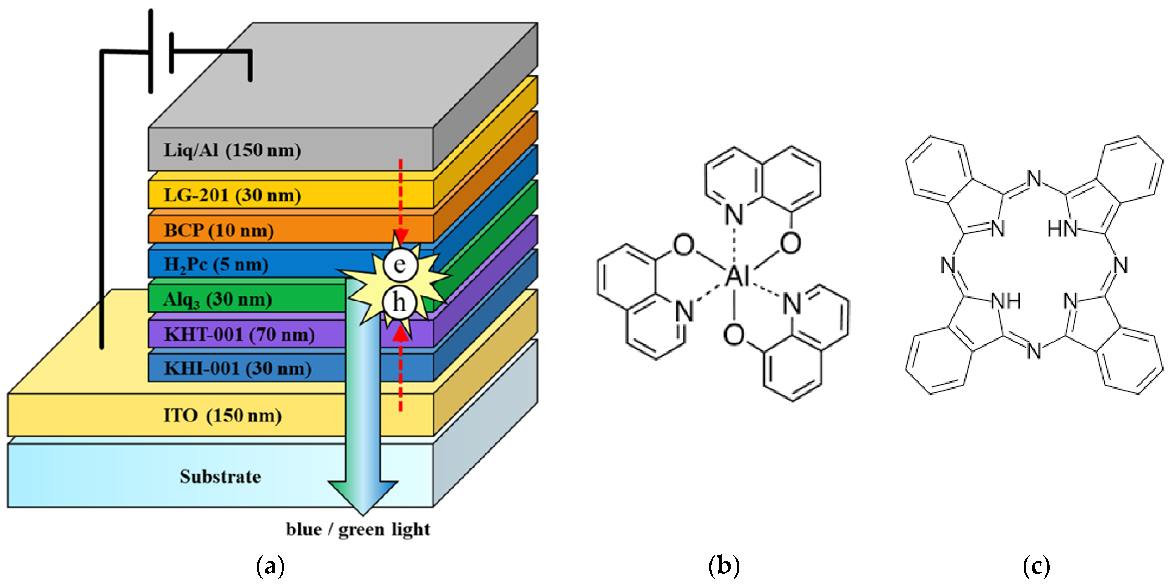
2. Experiment
3. Results and Discussions
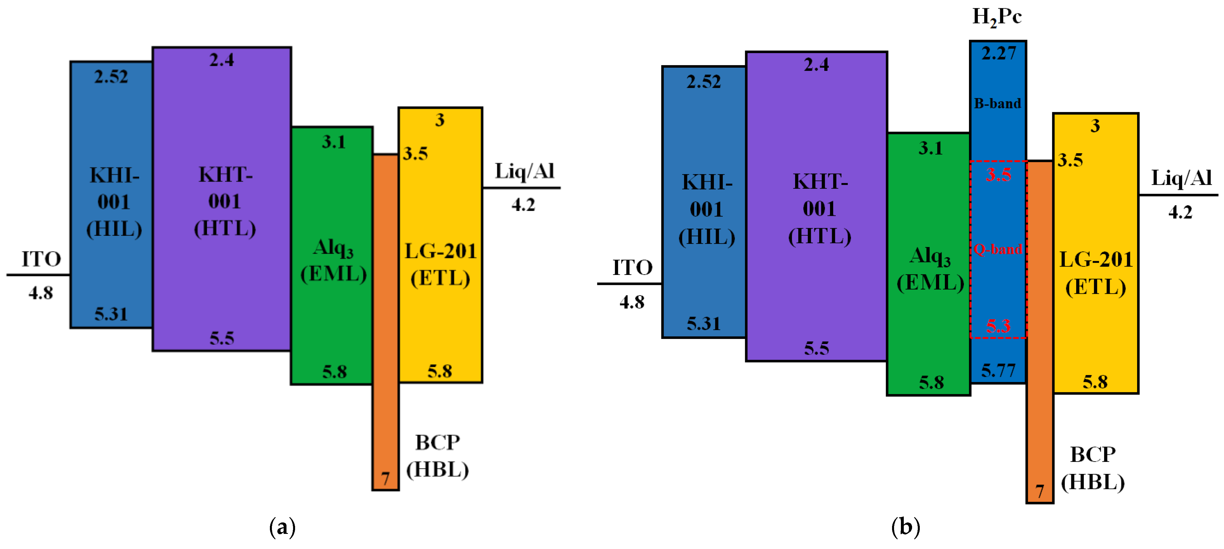
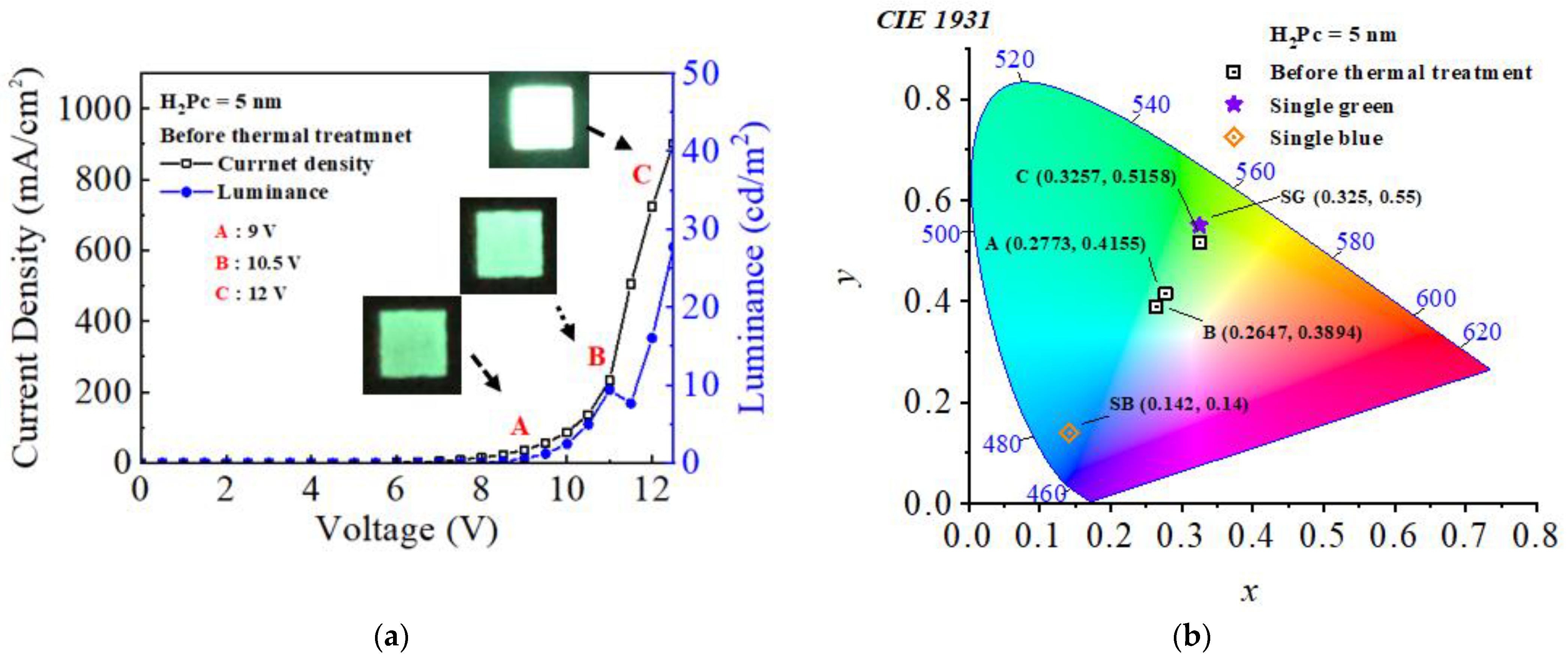
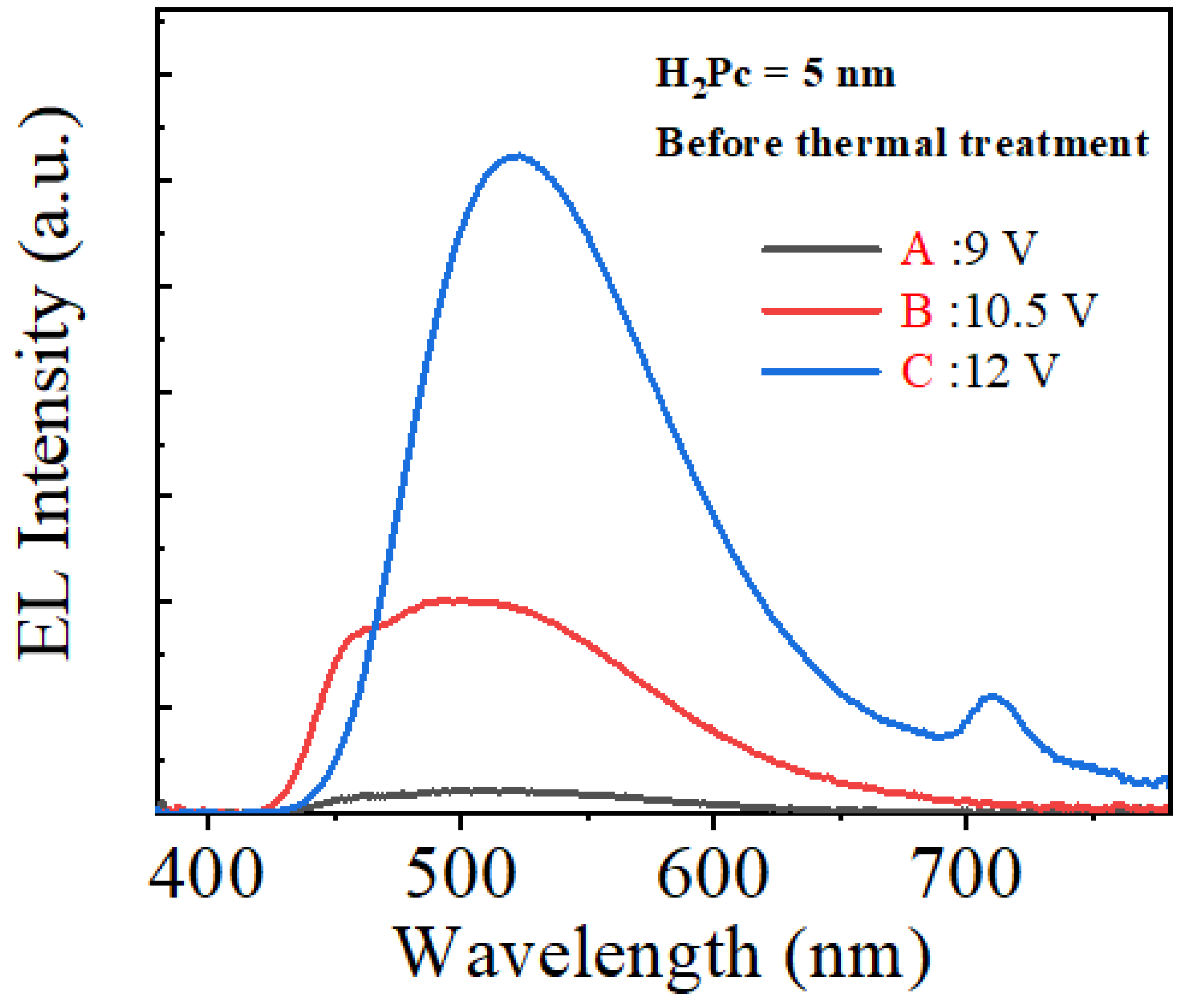
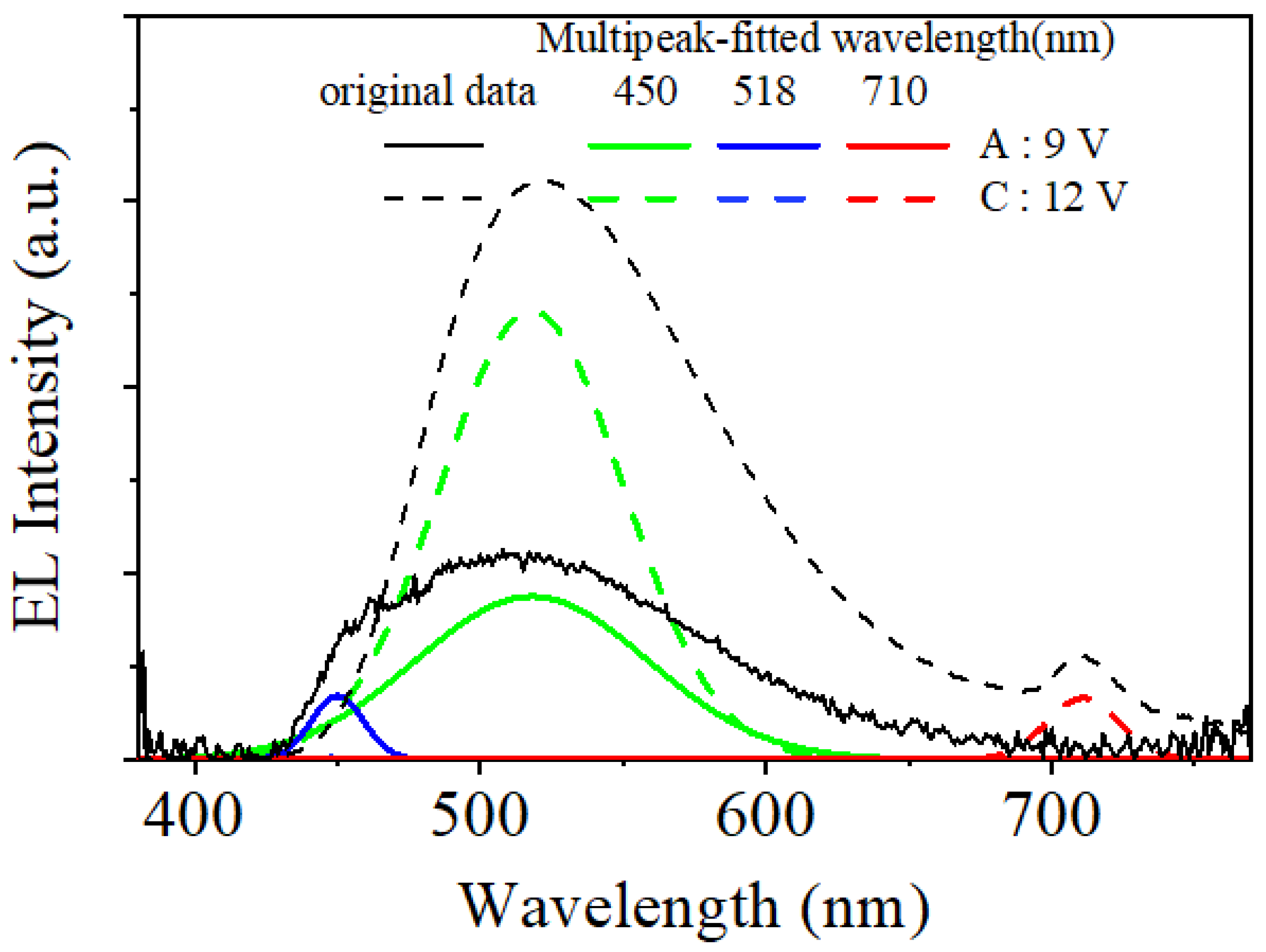
3.1. Characterization of the CTOLED before Thermal Treatment
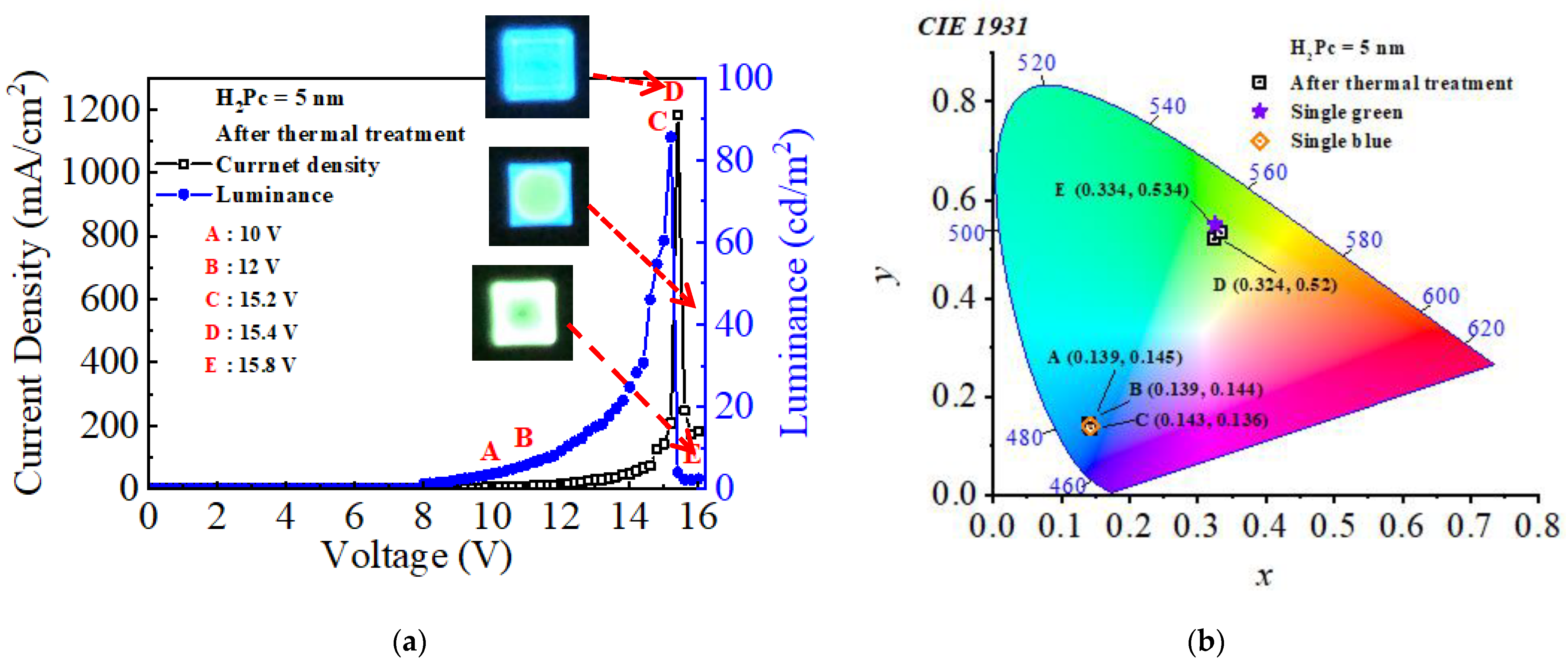
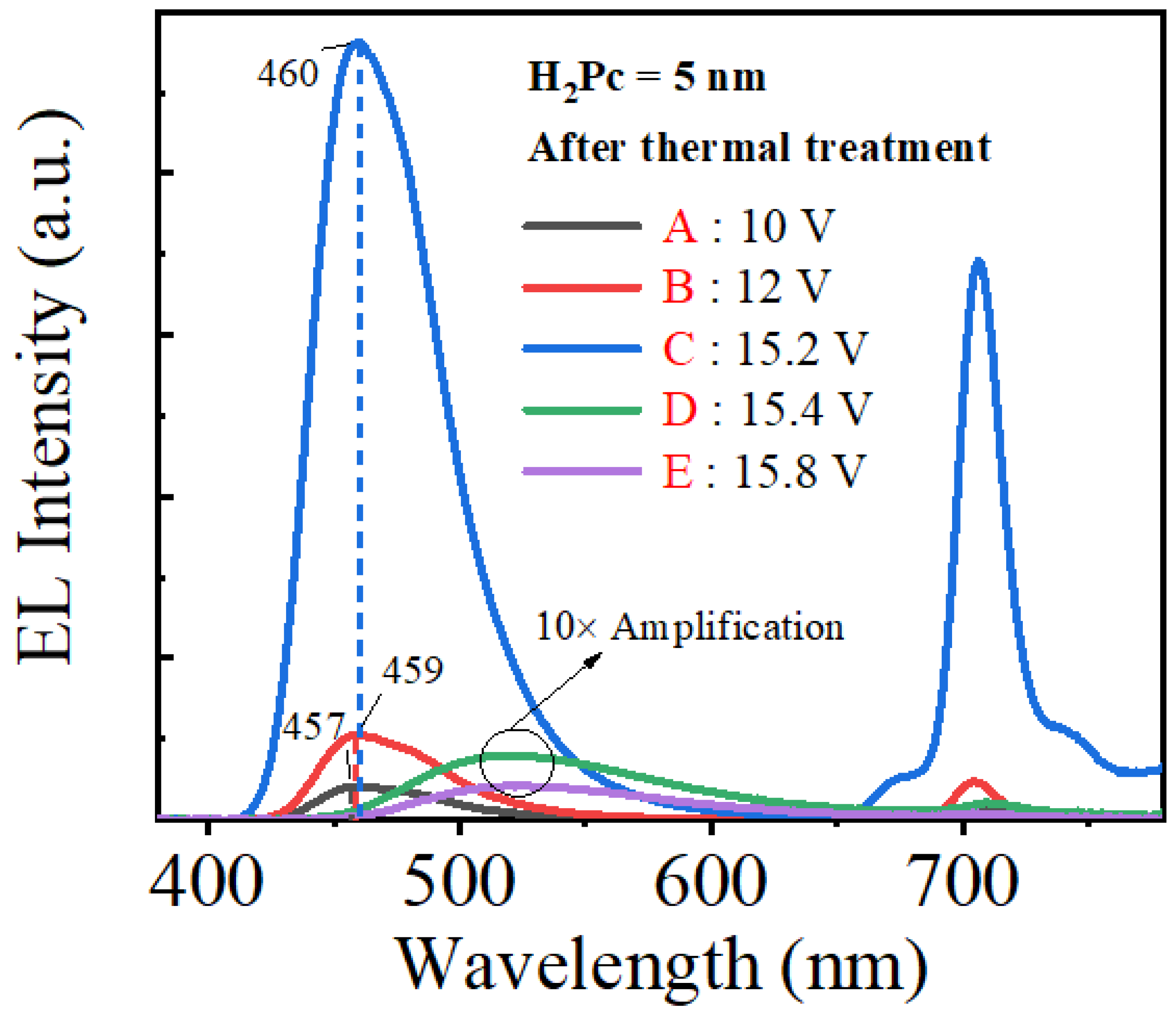
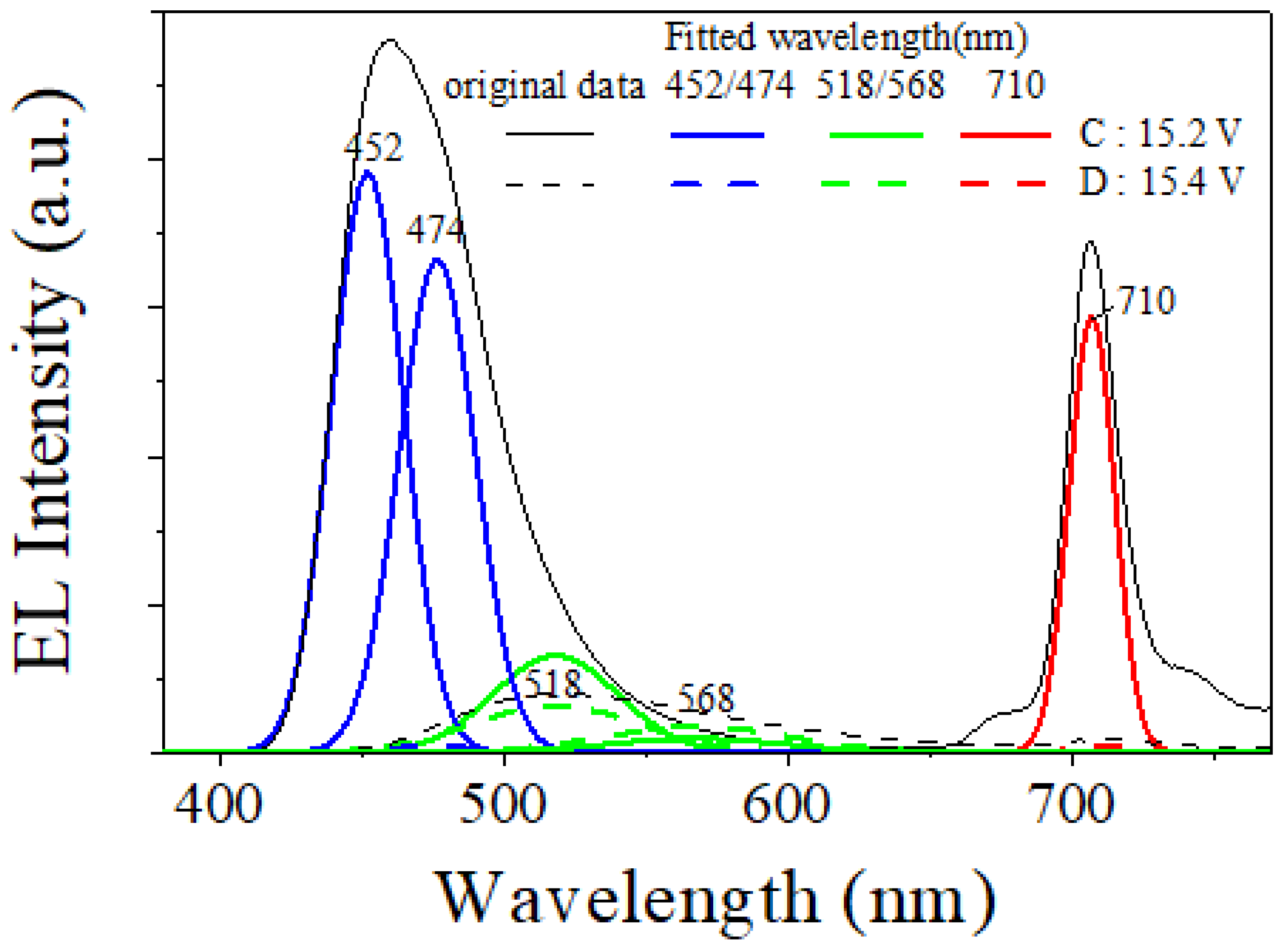
3.2. Characterization of the CTOLED after Thermal Treatment
3.3. Analysis of Thermal Treatment Effect
4. Conclusions
Author Contributions
Funding
Data Availability Statement
Acknowledgments
Conflicts of Interest
References
- Geffroy, B.; Roy, P.; Prat, C. Organic light-emitting diode (OLED) technology: Materials, devices and display technologies. Polym. Int. 2006, 55, 572–582. [Google Scholar] [CrossRef]
- Singh, M.; Jou, J.-H.; Sahoo, S.; Sujith, S.S.; He, Z.-K.; Krucaite, G.; Grigalevicius, S.; Wang, C.W. High light-quality OLEDs with a wet-processed single emissive layer. Sci. Rep. 2018, 8, 7133. [Google Scholar] [CrossRef] [PubMed] [Green Version]
- Shin, H.J.; Takasugi, S.; Park, K.-M.; Choi, S.-H.; Jeong, Y.-S.; Song, B.-C.; Kim, H.-S.; Oh, C.-H.; Ahn, B.-C. 7.1: Invited Paper: Novel OLED display technologies for large-size UHD OLED TVs. SID Symp. Dig. Tech. Pap. 2015, 46, 53–56. [Google Scholar] [CrossRef]
- So, F.; Kido, J.; Burrows, P. Organic light-emitting devices for solid-state lighting. MRS Bull. 2011, 33, 663–669. [Google Scholar] [CrossRef]
- Pu, Y.J.; Nakata, G.; Satoh, F.; Sasabe, H.; Yokoyama, D.; Kido, J. Optimizing the charge balance of fluorescent organic light-emitting devices to achieve high external quantum efficiency beyond the conventional upper limit. Adv. Mater. 2012, 24, 1765–1770. [Google Scholar] [CrossRef]
- Ji, W.; Zhao, J.; Sun, Z.; Xie, W. High-color-rendering flexible top-emitting warm-white organic light emitting diode with a transparent multilayer cathode. Org. Electron. 2011, 12, 1137–1141. [Google Scholar] [CrossRef]
- Xia, S.C.; Kwong, R.C.; Adamovich, V.I.; Weaver, M.S.; Brown, J. OLED Device Operational Lifetime: Insights and Challenges. In Proceedings of the 2007 IEEE International Reliability Physics Symposium, Phoenix, AZ, USA, 15–19 April 2007; pp. 253–257. [Google Scholar]
- Brutting, W.; Frischeisen, J.; Schmidt, T.D.; Scholz, B.J.; Mayr, C. Device efficiency of organic light-emitting diodes: Progress by improved light outcoupling. Phys. Status Solidi A 2012, 210, 44–65. [Google Scholar] [CrossRef]
- Kim, H.-G.; Kim, K.-H.; Kim, J.-J. Highly efficient, conventional, fluorescent organic light-emitting diodes with extended lifetime. Adv. Mater. 2017, 29, 1702159. [Google Scholar] [CrossRef]
- He, G.; Rothe, C.; Murano, S.; Werner, A.; Zeika, O.; Brinstock, J. White stacked OLED with 38 lm/W and 100,000-hour lifetime at 1000 cd/m2 for display and lighting applications. J. Soc. Inf. Disp. 2012, 17, 159–165. [Google Scholar] [CrossRef]
- Ide, N.; Tsuji, H.; Ito, N.; Matsuhisa, Y.; Houzumi, S.; Nishimori, T. White OLED Devices and Processes for Lighting Applications. In Proceedings of the SPIE Photonics Europe, Brussels, Belgium, 18 May 2010; pp. 772202.1–772202.8. [Google Scholar]
- Komoda, T.; Tsuji, H.; Yamae, K.; Varutt, K.; Matsuhisa, Y.; Ide, N. High performance white OLEDs for next generation solid state lightings. SID Symp. Dig. Tech. Pap. 2012, 42, 1056–1059. [Google Scholar] [CrossRef]
- Park, J.W.; Shin, D.C.; Park, S.H. Large-area OLED lightings and their applications. Semicond. Sci. Technol. 2011, 26, 034002. [Google Scholar] [CrossRef]
- Huang, Y.; Hsiang, E.-L.; Deng, M.-Y.; Wu, S.-T. Mini-LED, Micro-LED and OLED displays: Present status and future perspectives. Light Sci. Appl. 2020, 9, 105. [Google Scholar] [CrossRef] [PubMed]
- Sugimoto, A.; Ochi, H.; Fujimura, S.; Yoshida, A.; Miyadera, T.; Tsuchida, M. Flexible OLED displays using plastic substrates. IEEE J. Sel. Top. Quantum Electron. 2004, 10, 107–114. [Google Scholar] [CrossRef]
- Auch, M.D.J.; Soo, O.K.; Ewald, G.; Soo-Jin, C. Ultrathin glass for flexible OLED application. Thin Solid Film. 2002, 417, 47–50. [Google Scholar] [CrossRef]
- Yang, C.M.; Kim, C.W.; Kwon, H.J.; Kim, M.C.; Kim, P.R. Evaluation of perceived see-through level for transparent OLED displays. SID Symp. Dig. Tech. Pap. 2017, 48, 1363–1366. [Google Scholar] [CrossRef]
- Lee, J.-K.; Yim, J.-H. Alternating current input LED lighting control system using Fuzzy theory. J. Inf. Commun. Converg. Eng. 2021, 19, 214–220. [Google Scholar] [CrossRef]
- Cupkova, D.; Kajati, E.; Mocnej, J.; Papcun, P.; Koziorek, J.; Zolotova, I. Intelligent human-centric lighting for mental wellbeing improvement. Int. J. Distrib. Sens. Netw. 2019, 15, 1550147719875878. [Google Scholar] [CrossRef]
- Pelowski, M.; Graser, A.; Specker, E.; Forster, M.; Hinuber, J.V.; Leder, H. Does gallery lighting really have an impact on appreciation of art? An ecologically valid study of lighting changes and the assessment and emotional experience with representational and abstract paintings. Front. Psychol. 2019, 10, 2148. [Google Scholar] [CrossRef]
- Burrows, P.E.; Forrest, S.R.; Sibley, S.P.; Thompson, M.E. Color-tunable organic light-emitting devices. Appl. Phys. Lett. 1996, 69, 2959–2962. [Google Scholar] [CrossRef]
- Yang, Y.; Pei, Q. Voltage controlled two color light-emitting electrochemical cells. Appl. Phys. Lett. 1996, 68, 2708–2711. [Google Scholar] [CrossRef]
- Huang, C.C.; Meng, H.F.; Ho, G.K.; Chen, C.H. Color-tunable multilayer light-emitting diodes based on conjugated polymers. Appl. Phys. Lett. 2004, 84, 1195–1198. [Google Scholar] [CrossRef] [Green Version]
- Frobel, M.; Schwab, T.; Kliem, M.; Hofmann, S.; Leo, K.; Gather, M.C. Get it white: Color-tunable AC/DC OLEDs. Light Sci. Appl. 2015, 4, e247.1–e247.6. [Google Scholar] [CrossRef] [Green Version]
- Zhao, Y.; Chen, R.; Gao, Y.; Leck, K.S.; Yang, X.; Liu, S.; Abiyasa, A.P.; Divayana, Y.; Mutlugun, E.; Tan, S.T.; et al. AC-driven, color- and brightness-tunable organic light-emitting diodes constructed from an electron only device. Org. Electron. 2013, 14, 3195–3200. [Google Scholar] [CrossRef]
- Koo, J.H.; Jeong, S.J.; Shim, H.J.; Son, D.H.; Kim, J.M.; Kim, D.C.; Choi, S.J.; Hong, J.I.; Kim, D.H. Wearable electrocardiogram monitor using carbon nanotube electronics and color-tunable organic light-emitting diodes. ACS Nano 2017, 11, 10032–10041. [Google Scholar] [CrossRef] [PubMed]
- Xu, T.; Yang, M.; Liu, J.; Wu, X.; Murtaza, I.; He, G.; Meng, H. Wide color-range tunable and low roll-off fluorescent organic light emitting devices based on double undoped ultrathin emitters. Org. Electron. 2016, 37, 93–99. [Google Scholar] [CrossRef]
- Chen, K.; Wei, Z. High-efficiency single emissive layer color-tunable all-fluorescent white organic light-emitting diodes. Chem. Phys. Lett. 2022, 786, 139145. [Google Scholar] [CrossRef]
- Li, W.X.; Hagen, J.; Jones, R.; Heikenfeld, J.; Steckl, A.J. Color tunable organic light emitting diodes using Eu complex doping. Solid-State Electron. 2007, 51, 500–504. [Google Scholar] [CrossRef]
- Mao, M.; Lam, T.; To, W.; Lao, X.; Liu, W.; Xu, S.; Cheng, G.; Che, C. Stable, High-efficiency voltage-dependent color-tunable organic light-emitting diodes with a single tetradentate platinum(II) emitter having long operational lifetime. Adv. Mater. 2020, 33, 2004873. [Google Scholar] [CrossRef]
- Wang, Q.; Bai, J.; Zhao, C.; Ali, M.U.; Miao, J.; Meng, H. Simplified dopant-free color-tunable organic light-emitting diodes. Appl. Phys. Lett. 2021, 118, 253301. [Google Scholar] [CrossRef]
- Silvaco Int. ATLAS, version 5.32.1. R Manual; Silvaco Int.: Santa Clara, CA, USA, 2022. [Google Scholar]
- Tang, C.W.; VanSlyke, S.A. Organic electroluminescent diodes. Appl. Phys. Lett. 1987, 51, 913–915. [Google Scholar] [CrossRef]
- Fujii, A.; Yoshida, M.; Ohmori, Y.; Yoshino, K. Two-band electroluminescent emission in organic electroluminescent diode with phthalocyanine film. Jpn. J. Appl. Phys. 1996, 35, L37–L39. [Google Scholar] [CrossRef]
- El-Nahass, M.M.; Farid, A.M.; Attia, A.A.; Ali, H.A.M. Structural properties and UV to NIR absorption spectra of metal-free phthalocyanine (H2Pc) thin films. Fiz. A 2006, 15, 147–164. [Google Scholar]
- Fan, Z.; Cheng, C.; Yu, S.; Ye, K.; Sheng, R.; Xia, D.; Ma, C.; Wang, X.; Chang, Y.; Du, G. Red and near-infrared electroluminescence from organic light-emitting devices based on a soluble substituted metal-free phthalocyanine. Opt. Mater. 2009, 31, 889–894. [Google Scholar] [CrossRef]
- Yoon, J.-A.; Kim, Y.-H.; Kim, N.H.; Moon, C.-B.; He, G.; Kim, W.Y. Study of energy transfer in single and multi-emissive layer using Gaussian peak fitting. J. Lumin. 2014, 153, 104–108. [Google Scholar] [CrossRef]
- Park, T.J.; Lee, Y.K.; Kwon, S.K.; Kwon, J.H.; Jang, J. Resonant tunneling diode made of organic semiconductor superlattice. Appl. Phys. Lett. 2006, 89, 151114. [Google Scholar] [CrossRef]
- Zhu, Y.; Wang, H.; Chen, W.; Wang, Y.; Yan, D. Organic quantum wells with multiple negative differential resistance peaks and its photoswitch effect. Org. Electron. 2016, 35, 24–32. [Google Scholar] [CrossRef]
- El-Nahass, M.M.; Farid, A.M.; Attia, A.A.; Ali, H.A.M. Electrical transport properties of thermally evaporated phthalocyanine (H2Pc) thin films. Appl. Surf. Sci. 2006, 252, 7553–7561. [Google Scholar] [CrossRef]
- Mindorff, M.S.; Brodie, D.E. Some properties of metal-free amorphous phthalocyanine vacuum deposited films. Can. J. Phys. 1981, 59, 249–254. [Google Scholar] [CrossRef]
- Lee, E.K. Simulation of the thin-film thickness distribution for an OLED thermal evaporation process. Vacuum 2009, 83, 848–852. [Google Scholar] [CrossRef]
- Ji, Y.; Wang, M.; Yang, Z.; Ji, S.; Qiu, H. Nanowire-assisted self-assembly of one-dimensional nanocrystal superlattice chains. J. Mater. Chem. C 2019, 7, 8471–8476. [Google Scholar] [CrossRef]


Disclaimer/Publisher’s Note: The statements, opinions and data contained in all publications are solely those of the individual author(s) and contributor(s) and not of MDPI and/or the editor(s). MDPI and/or the editor(s) disclaim responsibility for any injury to people or property resulting from any ideas, methods, instructions or products referred to in the content. |
© 2022 by the authors. Licensee MDPI, Basel, Switzerland. This article is an open access article distributed under the terms and conditions of the Creative Commons Attribution (CC BY) license (https://creativecommons.org/licenses/by/4.0/).
Share and Cite
Ahn, T.J.; Choi, B.H.; Yu, J.-W.; Kim, Y.B.; Yu, Y.S. Effects of Thermal Treatment on DC Voltage-Driven Color Conversion in Organic Light-Emitting Diode. Micromachines 2023, 14, 30. https://doi.org/10.3390/mi14010030
Ahn TJ, Choi BH, Yu J-W, Kim YB, Yu YS. Effects of Thermal Treatment on DC Voltage-Driven Color Conversion in Organic Light-Emitting Diode. Micromachines. 2023; 14(1):30. https://doi.org/10.3390/mi14010030
Chicago/Turabian StyleAhn, Tae Jun, Bum Ho Choi, Jae-Woong Yu, Young Baek Kim, and Yun Seop Yu. 2023. "Effects of Thermal Treatment on DC Voltage-Driven Color Conversion in Organic Light-Emitting Diode" Micromachines 14, no. 1: 30. https://doi.org/10.3390/mi14010030