

High-Contrast Marking of Stainless-Steel Using Bursts of Femtosecond Laser Pulses

Abstract
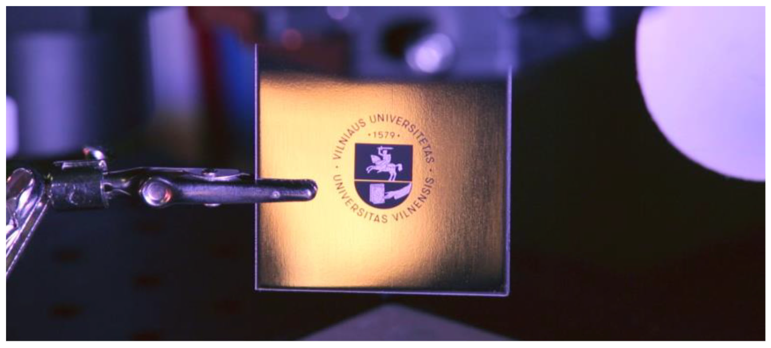
:1. Introduction
2. Materials and Methods
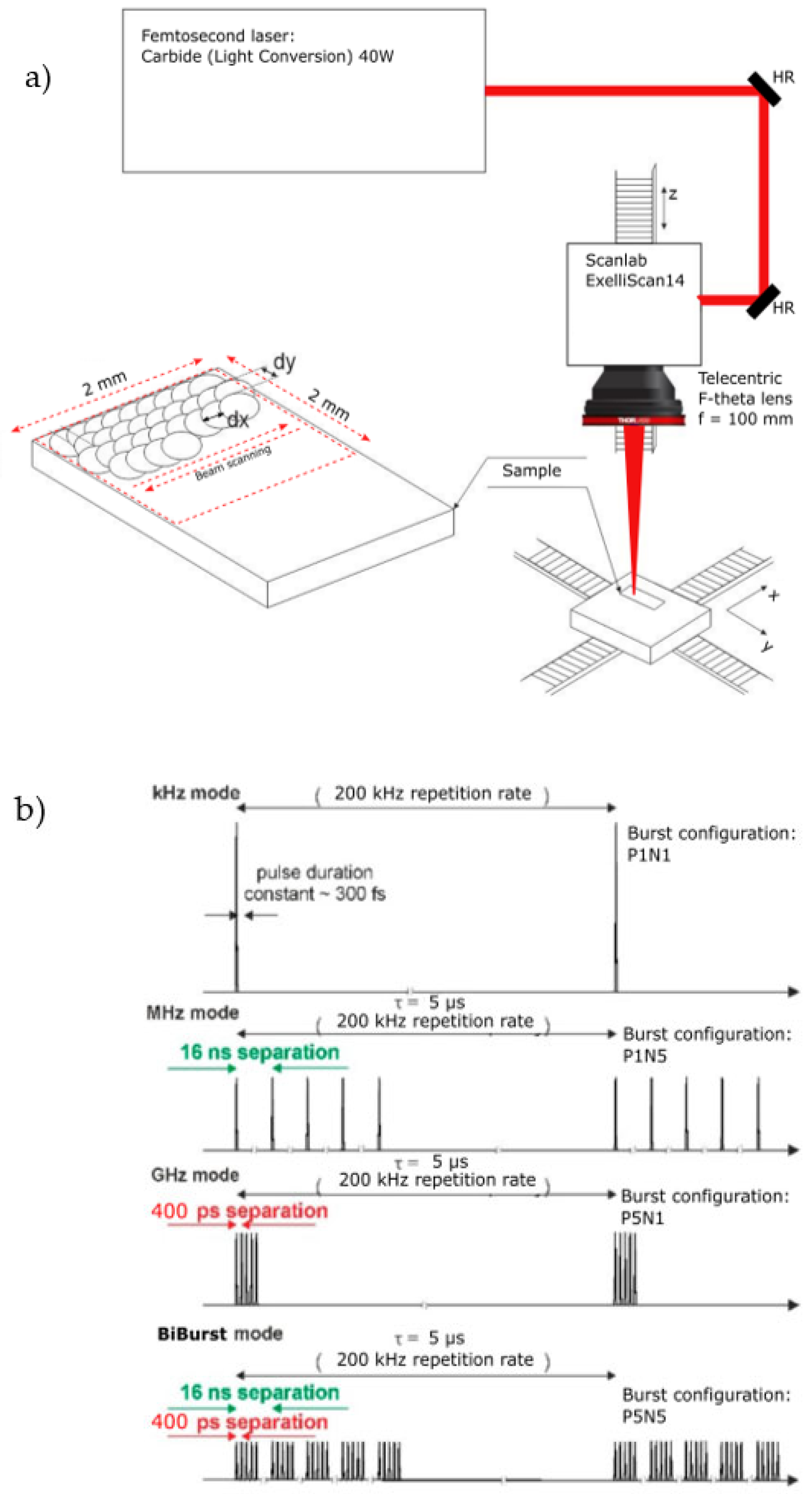
2.1. Experimental Setup for Ablation of Metal Sheets
2.2. Theoretical Insights into the Formation of Lambertian Scattering White Surfaces
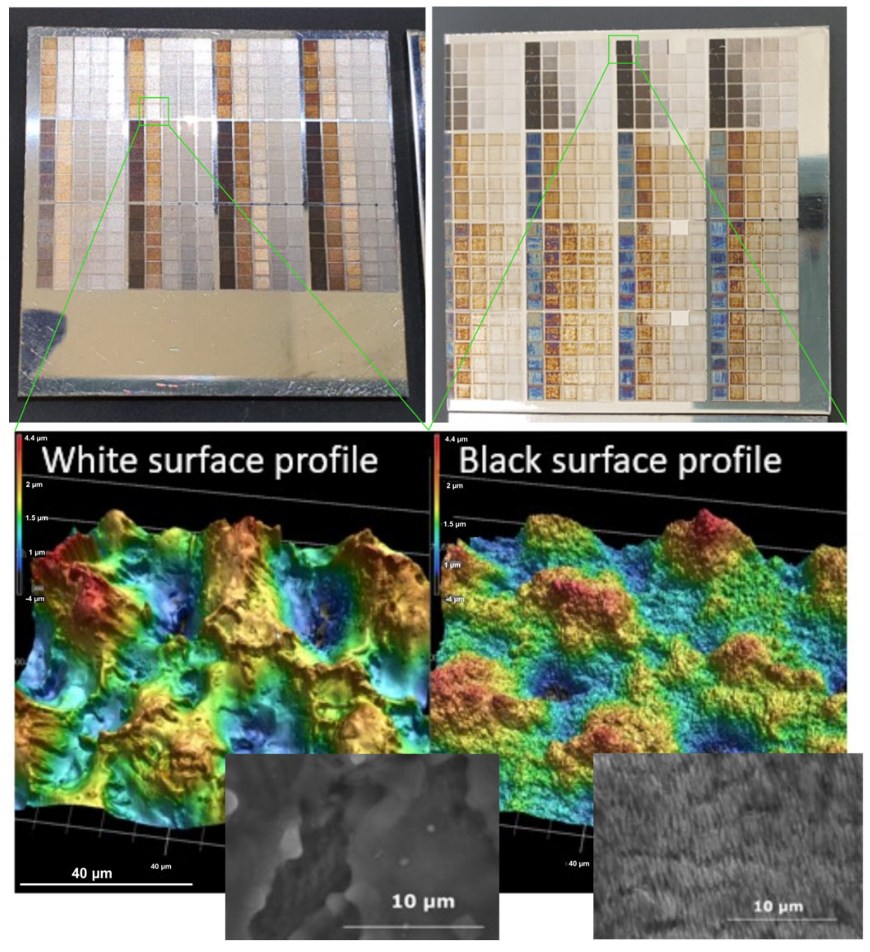
- Change in the height of the material due to manufactured irregularities should be larger than 150 nm, to induce scattering over the full angular spectrum;
- The distance between the formed dimples in the transverse coordinates (X and Y) should be smaller than 10 µm to manufacture a uniform scattering surface. The area between the dimples must have a low roughness <30 nm (Ra) to avoid a multiple reflection scenario which would increase light absorption on the surface.
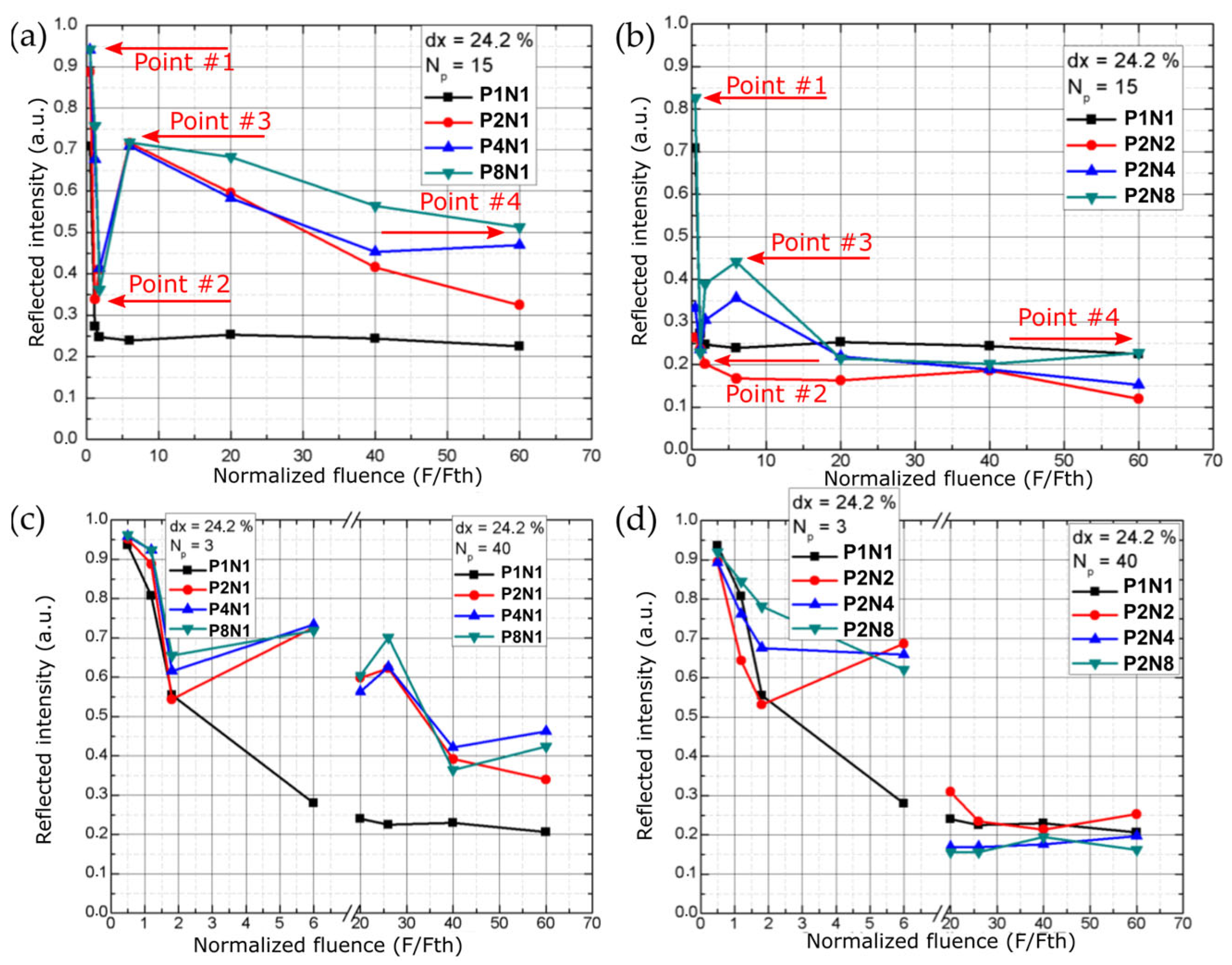
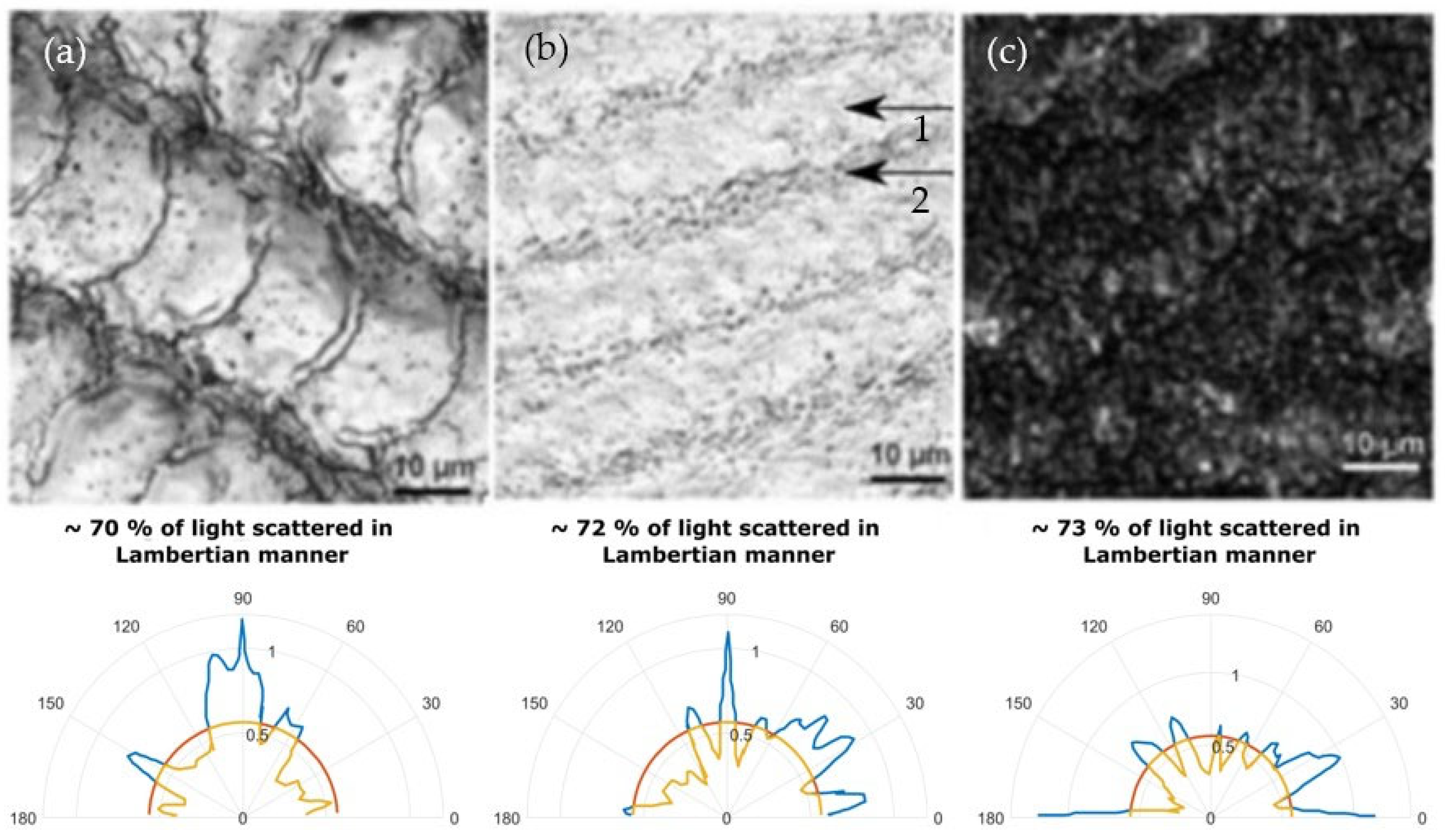
3. Results and Discussion
4. Conclusions
Author Contributions
Funding
Data Availability Statement
Conflicts of Interest
References
- Ding, K.; Wang, C.; Li, S.; Zhang, X.; Lin, N.; Duan, J. Single-Step Femtosecond Laser Structuring of Multifunctional Colorful Metal Surface and Its Origin. Surf. Interfaces 2022, 34, 102386. [Google Scholar] [CrossRef]
- Lazov, L.; Deneva, H.; Narica, P. Laser Marking Methods. Environ. Technol. Resour. Proc. Int. Sci. Pract. Conf. 2015, 1, 108. [Google Scholar] [CrossRef]
- Žemaitis, A.; Gaidys, M.; Gečys, P.; Barkauskas, M.; Gedvilas, M. Femtosecond Laser Ablation by Bibursts in the MHz and GHz Pulse Repetition Rates. Opt. Express 2021, 29, 7641. [Google Scholar] [CrossRef] [PubMed]
- Yue, T.M.; Yu, J.K.; Man, H.C. The Effect of Excimer Laser Surface Treatment on Pitting Corrosion Resistance of 316LS Stainless Steel. Surf. Coat. Technol. 2001, 137, 65–71. [Google Scholar] [CrossRef]
- Courant, B.; Hantzpergue, J.J.; Avril, L.; Benayoun, S. Structure and Hardness of Titanium Surfaces Carburized by Pulsed Laser Melting with Graphite Addition. J. Mater. Process. Technol. 2005, 160, 374–381. [Google Scholar] [CrossRef] [Green Version]
- Kwok, C.T. Laser Surface Alloying of Various Engineering Alloys for Sliding Wear and Corrosion Resistance. J. Laser Micro/Nanoeng. 2010, 5, 90–96. [Google Scholar] [CrossRef]
- Veiko, V.; Odintsova, G.; Vlasova, E.; Andreeva, Y.; Krivonosov, A.; Ageev, E.; Gorbunova, E. Laser Coloration of Titanium Films: New Development for Jewelry and Decoration. Opt. Laser Technol. 2017, 93, 9–13. [Google Scholar] [CrossRef]
- Jwad, T.; Deng, S.; Butt, H.; Dimov, S. Laser Induced Single Spot Oxidation of Titanium. Appl. Surf. Sci. 2016, 387, 617–624. [Google Scholar] [CrossRef]
- Khafaji, N.Y.; Demir, A.G.; Vitali, L.; Fustinoni, D.; Niro, A.; Previtali, B.; Taha, Z.A. Optical Characterization of Laser Coloured Titanium under Different Processing Atmospheres. Surf. Coat. Technol. 2017, 321, 156–163. [Google Scholar] [CrossRef]
- Long, J.; Fan, P.; Zhong, M.; Zhang, H.; Xie, Y.; Lin, C. Superhydrophobic and Colorful Copper Surfaces Fabricated by Picosecond Laser Induced Periodic Nanostructures. Appl. Surf. Sci. 2014, 311, 461–467. [Google Scholar] [CrossRef]
- Liu, Y.; Li, S.; Niu, S.; Cao, X.; Han, Z.; Ren, L. Bio-Inspired Micro-Nano Structured Surface with Structural Color and Anisotropic Wettability on Cu Substrate. Appl. Surf. Sci. 2016, 379, 230–237. [Google Scholar] [CrossRef]
- Gräf, S.; Kunz, C.; Undisz, A.; Wonneberger, R.; Rettenmayr, M.; Müller, F.A. Mechano-Responsive Colour Change of Laser-Induced Periodic Surface Structures. Appl. Surf. Sci. 2019, 471, 645–651. [Google Scholar] [CrossRef]
- Zhang, D.; Liu, R.; Li, Z. Irregular LIPSS Produced on Metals by Single Linearly Polarized Femtosecond Laser. Int. J. Extrem. Manuf. 2022, 4, 015102. [Google Scholar] [CrossRef]
- Zhang, D.; Li, X.; Fu, Y.; Yao, Q.; Li, Z.; Sugioka, K. Liquid Vortexes and Flows Induced by Femtosecond Laser Ablation in Liquid Governing Formation of Circular and Crisscross LIPSS. Opto-Electron. Adv. 2022, 5, 210066. [Google Scholar] [CrossRef]
- Huang, J.; Liu, Y.; Jin, S.; Wang, Z.; Qi, Y.; Zhang, J.; Wang, K.; Qiu, R. Uniformity Control of Laser-Induced Periodic Surface Structures. Front. Phys. 2022, 10, 932284. [Google Scholar] [CrossRef]
- Gräf, S. Formation of Laser-Induced Periodic Surface Structures on Different Materials: Fundamentals, Properties and Applications. Adv. Opt. Technol. 2020, 9, 11–39. [Google Scholar] [CrossRef]
- Vincenti, M.A.; Grande, M.; de Ceglia, D.; Stomeo, T.; Petruzzelli, V.; de Vittorio, M.; Scalora, M.; D’Orazio, A. Color Control through Plasmonic Metal Gratings. Appl. Phys. Lett. 2012, 100, 201107. [Google Scholar] [CrossRef] [Green Version]
- Shi, X.; Huang, Z.; Laakso, M.J.; Niklaus, F.; Sliz, R.; Fabritius, T.; Somani, M.; Nyo, T.; Wang, X.; Zhang, M.; et al. Quantitative Assessment of Structural and Compositional Colors Induced by Femtosecond Laser: A Case Study on 301LN Stainless Steel Surface. Appl. Surf. Sci. 2019, 484, 655–662. [Google Scholar] [CrossRef]
- Guay, J.-M.; Lesina, A.C.; Côté, G.; Charron, M.; Poitras, D.; Ramunno, L.; Berini, P.; Weck, A. Laser-Induced Plasmonic Colours on Metals. Nat. Commun. 2017, 8, 16095. [Google Scholar] [CrossRef]
- Ageev, E.I.; Bychenkov, V.Y.; Ionin, A.A.; Kudryashov, S.I.; Petrov, A.A.; Samokhvalov, A.A.; Veiko, V.P. Double-Pulse Femtosecond Laser Peening of Aluminum Alloy AA5038: Effect of Inter-Pulse Delay on Transient Optical Plume Emission and Final Surface Micro-Hardness. Appl. Phys. Lett. 2016, 109, 211902. [Google Scholar] [CrossRef]
- Gaudiuso, C.; Kämmer, H.; Dreisow, F.; Ancona, A.; Tünnermann, A.; Nolte, S.; Gaudiuso, C.; Kämmer, H.; Dreisow, F.; Ancona, A.; et al. Ablation of Silicon with Bursts of Femtosecond Laser Pulses. Front. Ultrafast Opt. Biomed. Sci. Ind. Appl. 2016, 9740, 974017. [Google Scholar] [CrossRef] [PubMed]
- Kramer, T.; Neuenschwander, B.; Jäggi, B.; Remund, S.; Hunziker, U.; Zürcher, J. Influence of Pulse Bursts on the Specific Removal Rate for Ultra-Fast Pulsed Laser Micromachining of Copper. Phys. Procedia 2016, 83, 123–134. [Google Scholar] [CrossRef] [Green Version]
- US6552301B2- Burst-Ultrafast Laser Machining Method- Google Patents. Available online: https://patents.google.com/patent/US6552301B2/en (accessed on 30 December 2022).
- Chu, K.; Guo, B.; Jiang, L.; Hua, Y.; Gao, S.; Jia, J.; Zhan, N. Throughput Improvement in Femtosecond Laser Ablation of Nickel by Double Pulses. Materials 2021, 14, 6355. [Google Scholar] [CrossRef] [PubMed]
- Andrusyak, O.G.; Bubelnik, M.; Mares, J.; McGovern, T.; Siders, C.W.; Andrusyak, O.G.; Bubelnik, M.; Mares, J.; McGovern, T.; Siders, C.W. Single-Pulse and Burst-Mode Ablation of Gold Films Measured by Quartz Crystal Microbalance. SPIE 2005, 5647, 61–71. [Google Scholar] [CrossRef]
- Butkus, S.; Jukna, V.; Paipulas, D.; Barkauskas, M.; Sirutkaitis, V. Micromachining of Invar Foils with GHz, MHz and KHz Femtosecond Burst Modes. Micromachines 2020, 11, 733. [Google Scholar] [CrossRef]
- Cheng, C.-W.; Chen, J.-K.; Kuo, C.-L.; Hsu, J.-C.; Ho, C.-C.; Chang, Y.-J. Drilling of Copper Using a Dual-Pulse Femtosecond Laser. Technologies 2016, 4, 7. [Google Scholar] [CrossRef] [Green Version]
- Ren, Y.; Cheng, C.W.; Chen, J.K.; Zhang, Y.; Tzou, D.Y. Thermal Ablation of Metal Films by Femtosecond Laser Bursts. Int. J. Therm. Sci. 2013, 70, 32–40. [Google Scholar] [CrossRef]
- Ionin, A.A.; Kudryashov, S.I.; Makarov, S.v.; Seleznev, L.v.; Sinitsyn, D.v. Generation and Detection of Superstrong Shock Waves during Ablation of an Aluminum Surface by Intense Femtosecond Laser Pulses. JETP Lett. 2011, 94, 34–38. [Google Scholar] [CrossRef]
- Supersonic Flow and Shock Waves-Richard Courant, K.O. Friedrichs-Google. Available online: https://books.google.lt/books?hl=lt&lr=&id=Qsxec0QfYw8C&oi=fnd&pg=PA1&ots=aMMJB_pgdi&sig=4mgcni-pBg3wTs0bJfj1TD1-Lus&redir_esc=y#v=onepage&q&f=false (accessed on 7 December 2022).
- Lin, Z.; Zhigilei, L.v.; Celli, V. Electron-Phonon Coupling and Electron Heat Capacity of Metals under Conditions of Strong Electron-Phonon Nonequilibrium. Phys. Rev. B Condens. Matter. Mater. Phys. 2008, 77, 075133. [Google Scholar] [CrossRef] [Green Version]
- Sandhu, A.S.; Dharmadhikari, A.K.; Kumar, G.R. Time Resolved Evolution of Structural, Electrical, and Thermal Properties of Copper Irradiated by an Intense Ultrashort Laser Pulse. J. Appl. Phys. 2004, 97, 023526. [Google Scholar] [CrossRef]
- Huang, J.; Zhang, Y.; Chen, J.K.; Huang, J.; Zhang, Y.; Chen, J.K. Superheating in Liquid and Solid Phases during Femtosecond-Laser Pulse Interaction with Thin Metal Film. Appl. Phys. A 2011, 103, 113–121. [Google Scholar] [CrossRef]
- Hess, H. Critical Data and Vapor Pressures for Aluminium and Copper. Int. J. Mater. Res. 2021, 89, 388–393. [Google Scholar] [CrossRef]
- Kelly, R.; Miotello, A. Comments on Explosive Mechanisms of Laser Sputtering. Appl. Surf. Sci. 1996, 96–98, 205–215. [Google Scholar] [CrossRef]
- US11276985B2-Device and Method for Generation of High Repetition Rate Laser Pulse Bursts-Google Patents. Available online: https://patents.google.com/patent/US11276985B2/en (accessed on 19 December 2022).
- Lakowicz, J.R. (Ed.) Principles of Fluorescence Spectroscopy; Springer: Boston, MA, USA, 2006; ISBN 978-0-387-31278-1. [Google Scholar]
- Pinel, N.; Bourlier, C.; Saillard, J. Degree of Roughness of Rough Layers: Extensions of the Rayleigh Roughness Criterion and Some Applications. Prog. Electromagn. Res. B 2010, 19, 41–63. [Google Scholar] [CrossRef] [Green Version]
- Kažukauskas, E.; Butkus, S.; Tokarski, P.; Jukna, V.; Barkauskas, M.; Sirutkaitis, V. Micromachining of Transparent Biocompatible Polymers Applied in Medicine Using Bursts of Femtosecond Laser Pulses. Micromachines 2020, 11, 1093. [Google Scholar] [CrossRef]


| Parameter | Setting, Value |
|---|---|
| F/Fth | 0.5, 0.7, 1.2, 1.8, 3, 4, 6, 14, 20, 26, 32, 40, 46, 53, 60 |
| Scanning overlap dx, dy (%) | 9, 24, 39, 54, 70 |
| # of repetitions (NP) | 1, 3, 6, 9, 12, 15, 20, 25, 30, 35, 40 |
| Burst configuration | P2N1, P4N1, P8N1, P2N2, P2N4, P2N8, P1N2, P1N4, P1N8 |
| Wavelength (nm) | 1030 |
| Laser rep. rate (kHz) | 200 |
Disclaimer/Publisher’s Note: The statements, opinions and data contained in all publications are solely those of the individual author(s) and contributor(s) and not of MDPI and/or the editor(s). MDPI and/or the editor(s) disclaim responsibility for any injury to people or property resulting from any ideas, methods, instructions or products referred to in the content. |
© 2023 by the authors. Licensee MDPI, Basel, Switzerland. This article is an open access article distributed under the terms and conditions of the Creative Commons Attribution (CC BY) license (https://creativecommons.org/licenses/by/4.0/).
Share and Cite
Butkus, S.; Jukna, V.; Kažukauskas, E.; Svirksas, Ž.; Paipulas, D.; Sirutkaitis, V. High-Contrast Marking of Stainless-Steel Using Bursts of Femtosecond Laser Pulses. Micromachines 2023, 14, 194. https://doi.org/10.3390/mi14010194
Butkus S, Jukna V, Kažukauskas E, Svirksas Ž, Paipulas D, Sirutkaitis V. High-Contrast Marking of Stainless-Steel Using Bursts of Femtosecond Laser Pulses. Micromachines. 2023; 14(1):194. https://doi.org/10.3390/mi14010194
Chicago/Turabian StyleButkus, Simas, Vytautas Jukna, Evaldas Kažukauskas, Žilvinas Svirksas, Domas Paipulas, and Valdas Sirutkaitis. 2023. "High-Contrast Marking of Stainless-Steel Using Bursts of Femtosecond Laser Pulses" Micromachines 14, no. 1: 194. https://doi.org/10.3390/mi14010194