Article

Investigation of Tunneling Effect for a N-Type Feedback Field-Effect Transistor

ICT & Robotics Engineering, Semiconductor Convergence Engineering, AISPC Laboratory and IITC, Hankyong National University, 327 Jungang-ro, Anseong-si 17579, Gyenggi-do, Korea
*
Author to whom correspondence should be addressed.
Micromachines 2022, 13(8), 1329; https://doi.org/10.3390/mi13081329
Submission received: 15 July 2022 / Revised: 6 August 2022 / Accepted: 15 August 2022 / Published: 16 August 2022
(This article belongs to the Special Issue 2D Semiconductor Materials and Devices)

Abstract

:
In this paper, the tunneling effect for a N-type feedback field-effect transistor (NFBFET) was investigated. The NFBFET has highly doped N-P junction in the channel region. When drain-source voltage is applied at the NFBFET, the aligning between conduction band of N-region and valence band of P-region occur, and band-to-band tunneling (BTBT) current can be formed on surface region of N-P junction in the channel of the NFBFET. When the doping concentration of gated-channel region (Ngc) is 4 × 1018 cm−3, the tunneling current makes off-currents increase approximately 104 times. As gate-source voltage is applied to NFBFET, the tunneling rate decreases owing to reducing of aligned region between bands by stronger gate-field. Eventually, the tunneling currents are vanished at the BTBT vanishing point before threshold voltage. When Ngc increase from 4 × 10¹⁸ to 6 × 10¹⁸, the tunneling current is generated not only at the surface region but also at the bulk region. Moreover, the tunneling length is shorter at the surface and bulk regions, and hence the leakage currents more increase. The BTBT vanishing point also increases due to increase of tunneling rates at surface and bulk region as Ngc increases.

1. Introduction

Recently, a metal oxide semiconductor field-effect transistor (MOSFET) has been challenged for limitation of switching speed and device scaling. Those challenges make hard to design next generation integrated circuits (ICs). In order to overcome these problem, novel devices, which have steep subthreshold slope (SS), were proposed, such as impact-ionization MOS (IMOS) [1,2,3], tunnel FET (TFET) [4,5,6,7], negative capacitance FET (NCFET) [8,9,10], and feedback FET (FBFET) [11,12].
Among them, the FBFET has been attracting attention as a next generation device, owing to complementary MOS (CMOS) based fabrication and high on/off ratio. The FBFET works on positive feedback, therefore, the FBFET has approximately zero subthreshold swing and hysteresis characteristics. Utilizing those characteristics, various circuits such as memory circuits, logic gates, bio-sensors, and neuromorphic circuits were presented [11,12,13,14,15,16,17,18,19,20,21,22,23,24,25,26,27,28,29,30]. Several structures of the FBFET have been proposed to meet the desired performance for each circuit. Most structures are based on S-shape energy band (or band-modulation) at the channel region. Mostly, the FBFET has P-N-P-N and P-N-i-N structure, and the family of Z2-FET, which is works on same mechanism, has P-i-N. The S-shape energy band consists of potential barrier and well. The potential barrier controls carrier injection at gated channel region. The carriers are injected by thermal emission to adjust the gate-source voltage. Then, the carriers are accumulated at ungated channel region. The accumulated carriers eliminate the potential well, and finally the carriers flow into the other side contact by diffusion. These mechanisms make the positive feedback between electron and hole in the channel region, and therefore the energy band of all regions is aligned. When the potential barrier and well are not high enough to make S-shape energy band, the FBFET works like a diode. Therefore, to make positive feedback in the channel region, highly doped region or virtually highly doped region are required. When a drain-source voltage is applied to the FBFET, the valence band of potential barrier and the conduction band of potential well were aligned, and the band-to-band tunneling (BTBT) current can be generated. The BTBT tunneling current make potential barrier and well lower, and therefore the leakage current increases and the threshold voltage changes. So far, when investigating the electrical characteristics of the FBFET using technology computer aided design (TCAD), physical models of MOSFET and bipolar junction transistor (BJT) were used according to FBFET structure. Most studies were not considered tunneling current in the channel region. To accurately investigate the electrical characteristics of the FBFET, it is necessary to consider the tunneling current that can have occurred at the channel region.
In this paper, the tunneling effect in the N-type FBFET(NFBFET) is investigated with various channel doping profiles. First, the energy band diagram for describing the simulation condition and the mechanism of FBFET will be introduced in Section 2. Then, simulation results of the electrical characteristics considering tunneling effect of the FBFET will be discussed in Section 3. Finally, conclusion will be described.

2. Simulation Results

2.1. Simulation Structure and Parameter

Figure 1 shows a 2-dimensional (2D) schematic diagram of NFBFET. The P-N-P-N structure was used for simulation, and the NFBFET was simulated with commercial simulator ATLAS by Silvaco [31]. Table 1 shows the structure parameter of the NFBFET. The doping concentration of gated-channel regions was variable. The material of the gate-oxide is aluminum oxide (Al2O3), and the work-function of the gate is 5.0 eV. For investigating the electrical characteristics for the NFBFET, the physical models of MOSFET and BJT were used. Those models include the transverse field dependent mobility model (CVT), field-dependent mobility (FLDMOB), Shockley-Read-Hall recombination model (SRH), Auger recombination model (AUGER), bandgap narrowing model (BGN), and Fermi-Dirac calculation model (FERMI). Additionally, for considering the tunneling effect, the non-local BTBT model (BBT.NONLOCAL) was used. The simulation was conducted by transient analysis, and the long term of time step (~1 s) was used to investigate DC characteristics of the NFBFET.

2.2. Mechanism of the NFBFET

Figure 2 shows the energy band diagram for describing the mechanism of the NFBFET. In this section, tunneling effect was not considered. For this structure, Ngc is 4 × 1018 cm−3. The black and red lines denote valence band and conduction band, respectively. Figure 2a shows the initial state of energy band diagram for NFBFET. For this state, the potential barrier formed by drain-source junction blocks carrier injection. When drain-source voltage (VDS) is applied to the NFBFET at 1 V, as shown in Figure 2b, carriers are injected into the channel region. When the gate-source voltage (VGS) is applied to the NFBFET with the forward sweep, the potential barrier is lower. The electron from source region can inject into channel region by thermal emission. The injected electrons accumulate at the potential well. As the VGS increases, the accumulated electrons increase, and then the potential well is eliminated. The hole from the drain region can inject into the channel region, as shown in Figure 2c. Finally, the conduction and valance bands of all regions are aligned, as shown in Figure 2d. The positive feedback occurs at threshold voltage accelerating the lowering barrier and well. Figure 3 shows the drain-source current-gate-source voltage (IDS-VGS) characteristics at VDS = 1 V. In the subthreshold region, off-current is made by minority carrier diffusion at drain-side junction. While the VGS increases, the leakage current increases by lowered potential well. Finally, the current increases rapidly by accelerating positive feedback near the threshold voltage, as shown in Figure 3.

3. Tunneling Effect for the NFBFET

The NFBFET has highly doped N-P junction in the channel region. When the VDS is applied to NFBFET such that the conduction band of the N-region and the valence band of the P-region are aligned, the BTBT can occur at N-P junction in the channel region, as shown in Figure 2b. Then, the BTBT currents make the carrier concentration in channel region change. Therefore, it is necessary to investigate the tunneling effect in the channel region.
Figure 4 shows IDS-VGS characteristics of NFBFET at VDS = 1 V when the BTBT is considered and ignored. The solid and dash lines denote simulation results considering and ignoring the BTBT, respectively. The leakage current considering BTBT increases about 104 times compared to ignoring BTBT when VGS = 0 V. As VGS increases, the conduction and valance bands of the gated channel region decrease, and then the BTBT current decreases due to increase of tunneling length at N-P junction in the channel region.

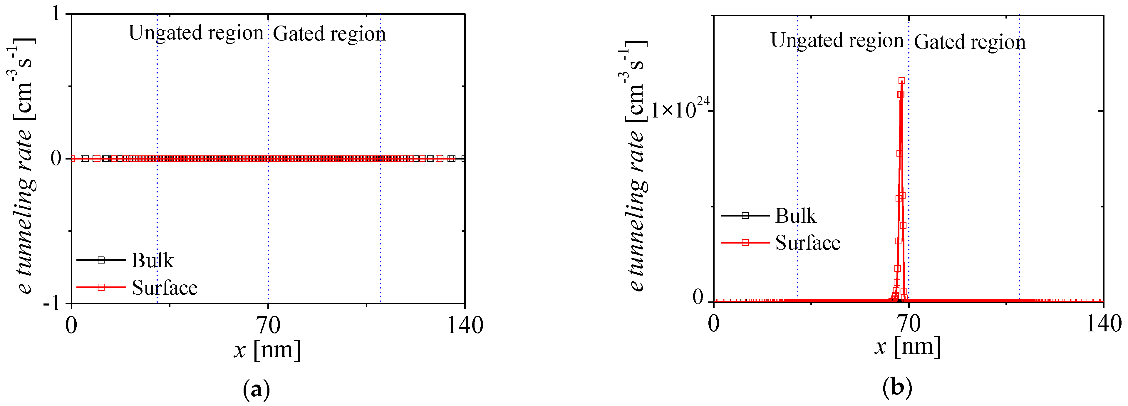
3.1. VDS Dependence of Leakage Current

Figure 5a,b show the electron tunneling rate of the NFBFET at two cases of VDS and fixed VGS = 0 V when the BTBT is considered. The black and red square-lines denote tunneling rates on bulk and surface regions, respectively. For the initial state (VDS = 0 V), there is no BTBT, as shown in Figure 5a. When VDS is applied at 1 V, the tunneling rate increase to approximately 1024 cm−3s−1, as shown in Figure 5b. Moreover, the BTBT occurs on the surface near N-P junction in the channel region due to band-bending by gate work-function difference in metal-oxide-semiconductor structure.
Figure 6a,b show the carrier concentrations on surface region of the NFBFET at two cases of VDSs and fixed VGS = 0 V when the BTBT is considered. The red and black lines denote electron and hole concentrations, respectively. The solid and dash lines denote concentrations with BTBT and non-BTBT, respectively. The carrier concentration of initial state is determined by doping concentration due to no BTBT currents, as shown in Figure 6a. The changed carrier concentrations at VDS = 1 V are shown in Figure 6b. When VDS increases, BTBT occurs on the surface of channel region. Excess carriers, which are generated by BTBT, are hard to flow into the electrode, owing to high potential barriers of drain and source-side junctions. Then, generated carriers accumulate in the channel region. Subsequently, accumulated carriers make the potential barrier and well of the channel region lower. Because lowered potential barrier permit injection from the source by thermal emission, the leakage current occurs. This mechanism is similar to the positive feedback.
Figure 7 show the energy bands on surface region at VGS = 0 and VDS = 1 V when BTBT is considered and ignored. The red and black lines denote conduction and valence bands, respectively. As shown in Figure 7, the potential barrier and well is shifted by changing carrier concentrations in the channel region. The shallowed potential well produces more minority carrier diffusion current at VGS = 0 V. Therefore, the leakage currents increase when the BTBT is considered, as shown in Figure 4.

3.2. VGS Dependence of Leakage Current

Figure 8a,b show the electron tunneling rates and energy band on surface region at VGS = 0.15 to 0.45 V with bias step of 0.1 V and VDS = 1 V. The black, red, green, and blue lines denote the electron tunneling rates and energy band at VGS = 0.15, 0.25, 0.35, and 0.45 V, respectively. The non-local tunneling process can be calculated with local tunneling process by assuming that the electric field is uniform at tunneling path [32]. When tunneling current with local process, the tunneling rate is related to tunneling length. For the Kane model, which is representative local model, the tunneling rate Gtun for BTBT is given by [33,34,35]
G tun = A k E g ( E g q W t ) 2.5 exp ( q B k W t E g ) ,
where Ak and Bk are nonlocal BTBT model parameter, and Eg and Wt are energy gap and tunneling length, respectively. The tunneling rate has an exponential relation with tunneling length. As VGS increases from 0.15 to 0.35 V, the tunneling rates decrease exponentially, owing to increase of tunneling length between conduction band of N-region and valence band of P-region by gate-field, as shown in Figure 8b. They reach zero approximately at VGS = 0.45 V, as shown in Figure 8a. Moreover, as the tunneling rates decrease, the electrons injected into potential well by BTBT decrease. Eventually, the change of potential well by BTBT is vanished, as shown in Figure 8b. Accordingly, the BTBT currents reduce as shown in Figure 4.
Figure 9a,b show the carrier concentrations on surface region at VGS = 0.35 and 0.45 V when BTBT is considered and ignored. The red and black lines denote electron and hole concentrations, respectively, and the solid and dash lines denote electron and hole concentrations with BTBT and non-BTBT, respectively. As shown in Figure 9a, carrier concentrations considering BTBT at VGS = 0.35 V are still some different from those ignoring BTBT, owing to remaining of BTBT at the surface. However, there is no longer a difference between carrier concentrations considering and ignoring BTBT when BTBT disappear at VGS = 0.45 V, as shown in Figure 9b. Therefore, as VGS increases, the current decreases, as shown in Figure 4. When VGS > 0.45 V, the current considering and ignoring BTBT are the same since BTBT does not exist, as shown in Figure 4.

3.3. Tunneling Effect with Various Doping Profile

Figure 10a shows the IDS-VGS characteristics of the NFBFET considering BTBT with Ngc from 4 × 10¹⁸ to 6 × 1018 cm−3 at VDS = 1 V. The filled and empty symbols denote the simulation results for considering and ignoring BTBT, respectively. As Ngc increases, the leakage current increases. When Ngc increase, the tunneling length is shorter, as shown in Figure 10b. Hence, the tunneling rates increase according to Equation (1). Moreover, higher Ngc make tunneling rates higher on surface as well as bulk region of the NFBFET, as shown in Figure 10c. However, as VGS increases, the BTBT currents decreases by lowering potential barrier on gated-channel region with stronger gate-field, and eventually they are vanished at BTBT vanishing points, as shown in Figure 10a, and then thermionic emission mechanism becomes dominant, such as the FBFET ignoring BTBT. The BTBT vanishing point increases due to increase of tunneling rates on surface and bulk region as Ngc increases.

4. Conclusions

The tunneling effect of the NFBFET was investigated in the case of Ngc of from 4 × 10¹⁸ to 6 × 1018 cm−3. First, when Ngc is 4 × 10¹⁸, the BTBT currents is generated on the surface region of the NFBFET. This BTBT currents make off-current increase about 104 times. As VGS increases, the BTBT currents decrease by lowering potential barriers on the gated-channel region with stronger gate-field, and eventually BTBT currents are vanished, and then thermionic emission currents become dominant such as the FBFET ignoring BTBT. As Ngc increase from 4 × 10¹⁸ to 6 × 1018 cm−3, the tunneling length is shorter. Following the tunneling probability equation, tunneling rate increases as Ngc increases. Accordingly, the leakage currents increase due to increase of tunneling rate. Moreover, the BTBT currents can be generated on surface region as well as bulk region. As VGS increases, the BTBT currents are also vanished before the threshold voltage, and the BTBT vanishing point increase as Ngc increases. According to these results, it is necessary to further investigate the tunneling effect of NFBFET on a very high doping channel region.

Author Contributions

Conceptualization, J.H.O. and Y.S.Y.; methodology, J.H.O. and Y.S.Y.; investigation, J.H.O. and Y.S.Y.; data curation, J.H.O.; writing—original draft preparation, J.H.O.; writing—review and editing, J.H.O. and Y.S.Y.; supervision, Y.S.Y.; project administration, Y.S.Y.; funding acquisition, Y.S.Y. All authors have read and agreed to the published version of the manuscript.

Funding

This research was supported by the Basic Science Research Program through NRF of Korea funded by the Ministry of Education (NRF-2019R1A2C1085295).

Acknowledgments

This work was supported by IDEC (EDA tool).

Conflicts of Interest

The authors declare no conflict of interest.

References

  1. Ramaswamy, S.; Kumar, M.J. Junctionless Impact Ionization MOS: Proposal and Investigation. IEEE Trans. Electron Devices 2014, 61, 4295–4298. [Google Scholar] [CrossRef]
  2. Sarkar, D.; Singh, N.; Banerjee, K. A Novel Enhanced Electric-Field Impact-Ionization MOS Transistor. IEEE Electron Device Lett. 2010, 31, 1175–1177. [Google Scholar] [CrossRef]
  3. Lahgere, A.; Kumar, M.J. The charge plasma n-p-n impact ionization MOS on FDSOI technology. IEEE Trans. Electron Devices 2017, 64, 3–7. [Google Scholar] [CrossRef]
  4. Ionescu, A.M.; Riel, H. Tunnel field-effect transistors as energy efficient electronic switches. Nature 2011, 479, 329–337. [Google Scholar] [CrossRef]
  5. Krishnamohan, T.; Kim, D.; Raghunathan, S.; Saraswat, K. Double-gate strained-Ge heterostructure tunneling FET (TFET) with record high drive currents and ≪60 mV/dec subthreshold slope. In Proceedings of the 2008 IEEE International Electron Devices Meeting (IEDM), San Francisco, CA, USA, 15–17 December 2008; pp. 1–3. [Google Scholar]
  6. Smith, J.T.; Das, S.; Appenzeller, J. Broken-gap tunnel MOSFET: A constant-slope sub-60-mV/decade transistor. IEEE Electron Device Lett. 2011, 32, 1367–1369. [Google Scholar] [CrossRef]
  7. Wang, L.; Yu, E.; Taur, Y.; Asbeck, P. Design of tunneling field-effect transistors based on staggered heterojunctions for ultralow-power applications. IEEE Electron Device Lett. 2010, 31, 431–433. [Google Scholar] [CrossRef]
  8. Rahi, S.B.; Tayal, S.; Upadhyay, A.K. A review on emerging negative capacitance field effect transistor for low power electronics. Microelectron. J. 2021, 116, 105242. [Google Scholar] [CrossRef]
  9. Khan, A.I.; Yeung, C.W.; Hu, C.; Salahuddin, S. Ferroelectric negative capacitance MOSFET: Capacitance tuning & antiferroelectric operation. In Proceedings of the 2011 International Electron Devices Meeting (IEDM), Washington, DC, USA, 5–7 December 2011; pp. 11.3.1–11.3.4. [Google Scholar]
  10. Lin, C.-I.; Khan, A.I.; Salahiddin, S.; Hu, C. Effects of the variation of ferroelectric properties on negative capacitance FET characteristics. IEEE Trans. Electron Devices 2016, 63, 2197–2199. [Google Scholar] [CrossRef]
  11. Padilla, A.; Yeung, C.W.; Shin, C.; Hu, C.; King Liu, T.-J.K. Feedback FET: A novel transistor exhibiting steep switching behavior at low bias voltages. In Proceedings of the 2008 IEEE International Electron Devices Meeting (IEDM), San Francisco, CA, USA, 15–17 December 2008; pp. 1–4. [Google Scholar]
  12. Yeung, C.W.; Padilla, A.; Liu, T.-J.K.; Hu, C. Programming characteristics of the steep turn-on/off feedback FET (FBFET). In Proceedings of the 2009 Symposium on VLSI Technology, Kyoto, Japan, 15–17 June 2009; pp. 176–177. [Google Scholar]
  13. Cho, J.; Lim, D.; Woo, S.; Cho, K.; Kim, S. Static random access memory characteristics of single-gated feedback field-effect transistors. IEEE Trans. Electron Devices 2019, 66, 413–419. [Google Scholar] [CrossRef]
  14. Woo, S.; Cho, J.; Lim, D.; Cho, K.; Kim, S. Transposable 3T-SRAM synaptic array using independent double-gate feedback field-effect transistor. IEEE Trans. Electron Devices 2019, 66, 4753–4758. [Google Scholar] [CrossRef]
  15. Kang, H.; Cho, J.; Kim, Y.; Lim, D.; Woo, S.; Cho, K.; Kim, S. Nonvolatile and volatile memory characteristics of a silicon nanowire feedback field-effect transistor with a nitride charge-storage layer. IEEE Trans. Electron Devices 2019, 66, 3342–3348. [Google Scholar] [CrossRef]
  16. Wan, J.; Le Royer, C.; Zaslavsky, A.; Cristoloveanu, S. Z2-FET used as 1-transistor high-speed DRAM. In Proceedings of the 2012 European Solid-State Device Research Conference (ESSDERC), Bordeaux, France, 17–21 September 2012; pp. 197–200. [Google Scholar]
  17. Martinie, S.; Lacord, J.; Rozeau, O.; Parihar, M.-S.; Lee, K.; Bawedin, M.; Cristoloveanu, S.; Taur, Y.; Barbe, J.-C. Z2-FET SPICE model: DC and memory operation. In Proceedings of the 2017 IEEE SOI-3D-Subthreshold Microelectronics Technology Unified Conference (S3S), Burlingame, CA, USA, 16–19 October 2017; pp. 1–3. [Google Scholar]
  18. Wan, J.; Le Royer, C.; Zaslavsky, A.; Cristoloveanu, S. Progress in Z2-FET 1T-DRAM: Retention time, writing modes, selective array operation, and dual bit storage. Solid State Electron. 2013, 84, 147–154. [Google Scholar] [CrossRef]
  19. Wan, J.; Le Royer, C.; Zaslavsky, A.; Cristoloveanu, S. Z2-FET: A zero-slope switching device with gate-controlled hysteresis. In Proceedings of the Technical program of 2012 VLSI Technology, System and Application, Hsinchu, Taiwan, 23–25 April 2012; pp. 1–4. [Google Scholar]
  20. El Dirani, H.; Solaro, Y.; Fonteneau, P.; Ferrari, P.; Cristoloveanu, S. Sharp-switching Z2-FET device in 14 nm FDSOI technology. In Proceedings of the 2015 45th European Solid State Device Research Conference (ESSDERC), Graz, Austria, 14–18 September 2015; pp. 250–253. [Google Scholar]
  21. Wan, J.; Le Royer, C.; Zaslavsky, A.; Cristoloveanu, S. A systematic study of the sharp-switching Z2-FET device: From mechanism to modeling and compact memory applications. Solid State Electron 2013, 90, 2–11. [Google Scholar] [CrossRef]
  22. Kim, M.; Kim, Y.; Lim, D.; Woo, S.; Cho, K.; Kim, S. Steep switching characteristics of single-gated feedback field-effect transistors. Nanotechnology 2016, 28, 055205. [Google Scholar] [CrossRef]
  23. Lee, C.; Ko, E.; Shin, C. Steep slope silicon-on-insulator feedback field-effect transistor: Design and performance analysis. IEEE Trans. Electron Devices 2019, 66, 286–291. [Google Scholar] [CrossRef]
  24. Oh, J.H.; Yu, Y.S. Investigation of monolithic 3D integrated circuit inverter with feedback field effect transistors using TCAD Simulation. Micromachines 2020, 11, 852. [Google Scholar] [CrossRef]
  25. Kwon, M.-W.; Hwang, S.; Baek, M.-H.; Cho, S.; Park, B.-G. Dual gate positive feedback field-effect transistor for low power analog circuit. In Proceedings of the 2017 Silicon Nanoelectronics Workshop (SNW), Kyoto, Japan, 4–5 June 2017; pp. 115–116. [Google Scholar]
  26. Lee, I.; Park, H.; Nguyen, Q.T.; Kim, G.; Cho, S.; Cho, I. Optimization of Feedback FET with Asymmetric Source Drain Doping profile. Micromachines 2022, 13, 508. [Google Scholar] [CrossRef]
  27. Singh, D.; Patil, G.C. Performance analysis of feedback field-effect transistor-based biosensor. IEEE Sens. J. 2020, 20, 13269–13276. [Google Scholar] [CrossRef]
  28. Kwon, M.-W.; Park, K.; Baek, M.-H.; Lee, J.; Park, B.-G. A low-energy high-density capacitor-less I&F neuron circuit using feedback FET Co-integrated with CMOS. IEEE J. Electron Devices Soc. 2019, 7, 1080–1084. [Google Scholar]
  29. Kwon, M.-W.; Park, K.; Park, B.-G. Low-power adaptive integrate-and-fire neuron circuit using positive feedback FET Co-Integrated with CMOS. IEEE Access 2021, 9, 159925–159932. [Google Scholar] [CrossRef]
  30. Woo, S.; Cho, J.; Lim, D.; Park, Y.-S.; Cho, K.; Kim, S. Implementation and characterization of an integrate-and-fire neuron circuit using a silicon nanowire feedback field-effect transistor. IEEE Trans. Electron Devices 2020, 67, 2995–3000. [Google Scholar] [CrossRef]
  31. Silvaco Int. ATLAS, ver. 5. 32. 1.; R Manual; Silvaco Int.: Santa Clara, CA, USA, 2021. [Google Scholar]
  32. Biswas, A.; Dan, S.S.; Le Royer, C.; Grabinski, W.; Ionescu, A.M. TCAD simulation of SOI TFETs and calibration of non-local band-to-band tunneling model. Microelectron. Eng. 2012, 98, 334–337. [Google Scholar] [CrossRef]
  33. Kane, O.E. Theory of tunneling. J. Appl. Phys. 1961, 32, 83–91. [Google Scholar] [CrossRef]
  34. Najam, F.; Yu, Y.S. Compact model for L-shaped tunnel field-effect transistor including the 2D region. Appl. Sci. 2019, 9, 3716. [Google Scholar] [CrossRef]
  35. Yu, Y.S.; Najam, F. Compact capacitance model of L-shape tunnel field-effect transistors for circuit simulation. J. Inf. Commun. Converg. Eng. 2021, 19, 263–268. [Google Scholar] [CrossRef]
Figure 1. 2D schematic diagram of the NFBFET.
Micromachines 13 01329 g001
Figure 2. Energy band diagrams of NFBFET of each state. (a) initial state (VDS = VGS = 0 V), (b) VGS = 0 V and VDS = 1 V, (c) forward sweep of gate−source voltage VGS at VDS = 1 V, (d) on−state by VGS at VDS = 1 V.
Micromachines 13 01329 g002aMicromachines 13 01329 g002b
Figure 3. Drain−source current − gate−source voltage (IDS-VGS) characteristics of NFBFET at VDS = 1 V.
Micromachines 13 01329 g003
Figure 4. Comparison of IDS-VGS characteristics of NFBFET between considering and ignoring the BTBT at VDS = 1 V.
Micromachines 13 01329 g004
Figure 5. Electron tunneling rates at two cases of VDS on bulk and surface regions. (a) VDS = 0 V (initial state) and (b) VDS = 1 V.
Micromachines 13 01329 g005
Figure 6. Comparison of carrier concentrations on surface region at two cases of VDS. (a) VDS = 0 V (initial state) and (b) VDS = 1.0 V.
Micromachines 13 01329 g006
Figure 7. Comparison of energy bands on surface region at VGS = 1 V and VDS = 1 V when BTBT is considered and ignored.
Micromachines 13 01329 g007
Figure 8. (a) Electron tunneling rates and (b) energy bands on surface region at VGS = 0.15 (black), 0.25 (red), 0.35 (green), and 0.45 V (blue) at VDS = 1 V.
Micromachines 13 01329 g008
Figure 9. Comparison of carrier concentrations on surface region when BTBT is considered and ignored at VDS = 1 V. (a) VGS = 0.35 V and (b) VGS = 0.45 V.
Micromachines 13 01329 g009
Figure 10. (a) Comparison of IDS-VGS characteristics of the NFBFET with Ngc from 4 × 10¹⁸ to 6 × 10¹⁸ between considering and ignoring the BTBT, (b) the energy band on the surface region for ignoring the BTBT near N−P junction in the channel region with Ngc from 4 × 10¹⁸ to 6 × 10¹⁸ at VDS = 1 V and VGS = 0 V, and (c) the tunneling rates from surface to bulk region of the NFBFET with Ngc from 4 × 10¹⁸ to 6 × 10¹⁸ at VDS = 1 V and VGS = 0 V.
Micromachines 13 01329 g010aMicromachines 13 01329 g010b
Table 1. Structure parameter of the NFBFET for TCAD simulation.
ParametersDescriptionValue/Unit
LdrainLength of drain region30 nm
LugcLength of ungated channel region40 nm
LugcLength of gated channel region40 nm
LsourceLength of source region30 nm
TsiThickness of silicon body15 nm
ToxThickness of gate-oxide3 nm
NgcDoping concentration of gated channel regionVar.
Doping concentration of P+ region1 × 1020 cm−3
Doping concentration of N+ region1 × 1020 cm−3
Publisher’s Note: MDPI stays neutral with regard to jurisdictional claims in published maps and institutional affiliations.

