Article

120 GHz Frequency-Doubler Module Based on GaN Schottky Barrier Diode

1
State Key Laboratory of Optoelectronic Materials and Technologies, School of Electronics and Information Technology, Sun Yat-sen University, Guangzhou 510275, China
2
Key Laboratory of Microwave Remote Sensing, National Space Science Center, Chinese Academy of Sciences, Beijing 100190, China
3
Science and Technology on Reliability Physics and Application of Electronic Component Laboratory, China Electronic Product Reliability and Environmental Testing Research Institute, Guangzhou 510640, China
4
State Key Laboratory for Mesoscopic Physics and Frontiers Science Center for Nano-Optoelectronics, School of Physics, Peking University, Beijing 100871, China
*
Author to whom correspondence should be addressed.
Micromachines 2022, 13(8), 1172; https://doi.org/10.3390/mi13081172
Submission received: 6 July 2022 / Revised: 22 July 2022 / Accepted: 23 July 2022 / Published: 25 July 2022
(This article belongs to the Special Issue Microwave Passive Components)

Abstract

:
Traditional GaAs-based frequency multipliers still exhibit great challenges to meet the demand for solid-state high-power THz sources due to low breakdown voltage and heat dissipation of the Schottky barrier diode (SBD). In this study, a GaN SBD chain was fabricated with n/n+-GaN structure. As a consequence, the breakdown voltage of 54.9 V at 1 μA and cut-off frequency of 587.5 GHz at zero bias were obtained. A 120 GHz frequency-doubler module based on the GaN SBD chain was designed and fabricated. When driven with 500 mW input power in a continuous wave, the output power of the frequency-doubler module was 15.1 mW at 120 GHz. Moreover, the experiments show that the frequency-doubler module can endure an input power of 2 W. In addition, it is worth noting that the SBD chain works well at an anode temperature of 337.2 °C.

1. Introduction

Terahertz (THz) sources are indispensable elements in the THz system. At present, the demand for solid-state high-power THz sources is expected in communications, non-destructive testing, Earth atmospheric remote sensing, and automotive radar sensors, etc. [1,2,3,4,5]. The traditional THz sources can produce high power, such as vacuum electronic devices, traveling wave tubes, quantum-cascade lasers (QCLs), and gyrotron. However, their applications are limited due to bottleneck problems, such as miniaturization, operation at room temperature, and integration with circuits [6,7]. The solid-state THz sources effectively solve these problems. They are most commonly operated by frequency multipliers of GaAs Schottky barrier diode (SBD), which realizes the nonlinear function inside waveguide. GaAs-based frequency multipliers have been achieved continuous wave (CW) sources, high stability, and reliability at room temperature [8,9,10,11,12,13,14]. The GaAs-based solid-state source can reach 2.7 THz by power amplifiers and power-combined frequency multiplier chips [6]. The output power of 250 mW was demonstrated for a short time using the 150 GHz doubler by ACST GmbH [11]. However, it is still a challenge for the GaAs-based frequency multipliers to meet requirements for high-power applications owing to the shortages of low breakdown voltage and heat dissipation. The following techniques have been adopted for the higher output power of the frequency multiplier, such as reducing heat dissipation by cooling [15], diamond substrate [16,17], film-diode technology [18,19], power-combining technology [20,21,22,23], and so on. However, these techniques result in complex THz sources architecture and higher costs.
Compared with GaAs material, GaN is a promising material for high-power THz sources due to its higher breakdown voltage and wide band gap (3.4 eV). However, there are few studies on GaN-based frequency multipliers in the THz field. Bo Zhang et al. obtained a THz source of 17.5 mW at 220 GHz by frequency tripler based on SBD of the n/n+-GaN structure [24]. Lisen Zhang et al. obtained a THz source of 1322 mW at 150 GHz by frequency doubler based on GaN SBD [25]. Nevertheless, the output power of the frequency doubler is obtained under the pulse waveform condition, which greatly limits the application of the THz source.
In this work, a GaN SBD chain with a breakdown voltage of 54.9 V was fabricated with the n/n+-GaN structure. A 120 GHz frequency-doubler module based on GaN-based SBD chain was designed and fabricated, which was based on the 3D model optimized by introducing parasitic parameters. The output power of the CW reached 15.1 mW at 120 GHz. In addition, the temperature distribution of the SBD chain was carried out to evaluate the reliability of the GaN-based SBD chain.

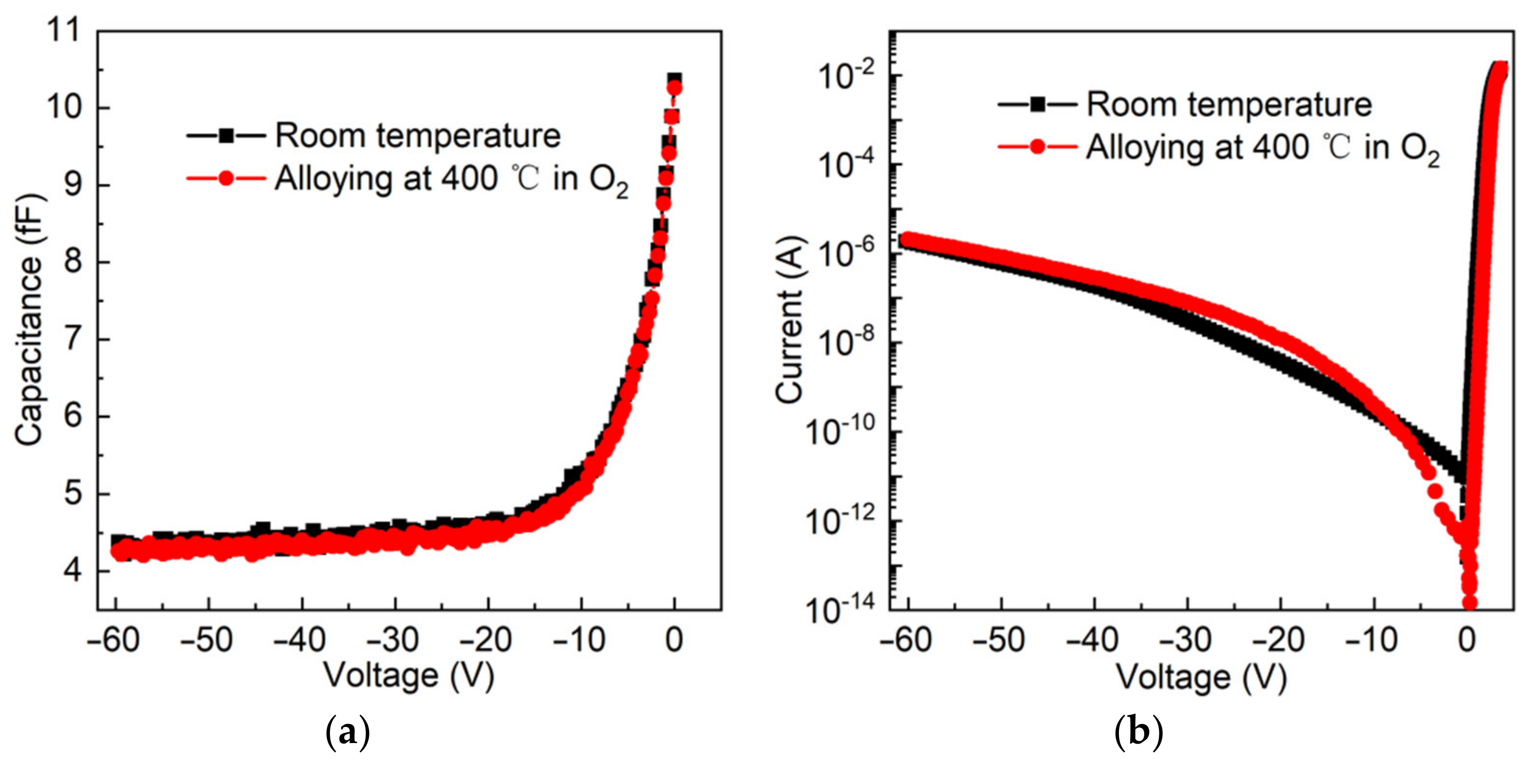
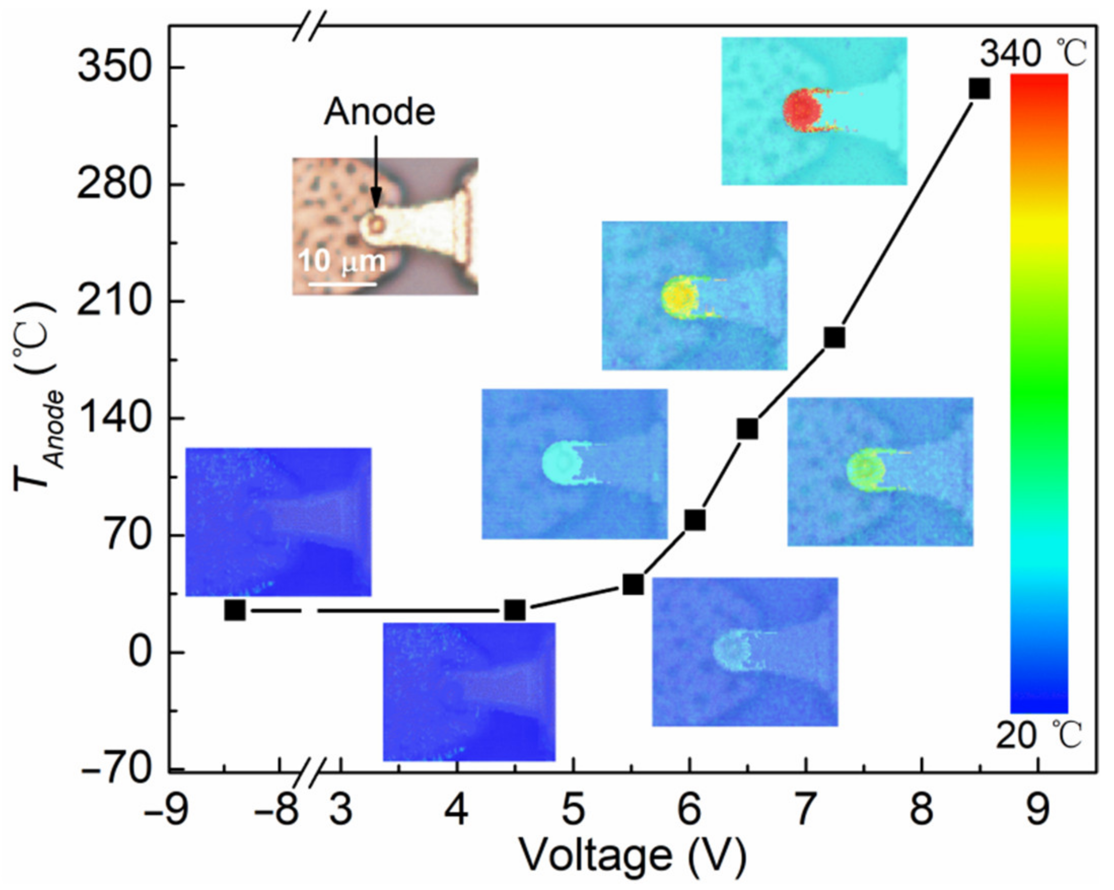
2. Design and Fabrication of GaN SBD Chain

In our design, a 120 GHz frequency-doubler module based on the GaN SBD chain uses the nonlinear effect of the SBD to produce the harmonics. The GaN SBD chains (parallel two chains of three series SBDs) were designed as depicted in Figure 1a. Figure 1b displays an optical micrograph of the SBD chain with the air-bridge SBD, and the overall chip is composed of six anodes with external sizes of 470 µm × 76 µm × 72 µm. An anode SBD with epitaxial information and parasitic parameters is shown in Figure 1c, which was grown by metal-organic chemical vapor deposition (MOCVD) on c-plane flat 2-inch sapphire. From bottom to top, the structure of sample consist of a 25 nm AlN, 450 nm GaN buffer layer, 2.3 μm n+-GaN with a Si doping concentration of 1019 cm−3, and 150 nm n-GaN with a Si doping concentration of 4 × 1017 cm−3. The quality of the GaN is measured by X-ray rocking curve. The FWHM of (002) and (102) planes are 121 and 303 arcsec, respectively. The screw and edge dislocation densities are calculated as 2.94 × 10⁷ and 4.88 × 108 cm−2, respectively [26]. GaN SBD chains were fabricated following mesa isolation by dry etching using inductively coupled plasma (ICP), cathodes metal by depositing Ti/Al/Ni/Au (15/80/20/60 nm) to n+-GaN, rapid thermal annealing in N2, Schottky metal with Ni/Au (50/100 nm), and electroplated 2.3 μm gold air-bridge. The sapphire substrate was thinned to 67 μm, and the GaN SBD chains were separated using stealth dicing technology.
The parasitic parameters reduce the conversion efficiency of the frequency multiplier, such as parasitic capacitance ( C p p + C f p ) and series resistance ( R e x p + R s p r e a d i n g + R c o n t a c t ), as shown in Figure 1c. To reduce parasitic parameters, the air-bridge GaN SBD with an anode diameter of 5 µm is adopted for a 120 GHz frequency doubler. The parasitic capacitance is reduced by deep mesa isolation and thin substrate. The values of pad-to-pad capacitance ( C p p ) and finger capacitance ( C f p ) are 3.0 fF and 1.1 fF, respectively. The series resistance is mainly from epitaxial resistance ( R e x p ). A high doping concentration of the n+-GaN layer can reduce the spreading resistance ( R s p r e a d i n g ) and ohmic contact resistance ( R c o n t a c t ). The resistivity of the n+-GaN layer is 2.8 × 10⁻³ Ω cm. The specific contact resistivity is 1.41 × 10⁻⁵ Ω cm2.
We measured the capacitance-voltage (C-V) and current-voltage (I-V) characteristics by the Keysight B1505A and Keithley 4200-SCS semiconductor parameter analyzer at room temperature (RT), respectively. The tests were performed at room temperature. Figure 2a,b shows experimental results of GaN SBDs with three anodes. It can be seen that both GaN SBDs with and without alloying exhibit good Schottky diode properties. There is no essential difference for the I-V and C-V curves between room temperature and after alloying of 400 °C in O2 ambient. The important parameters of GaN SBDs are almost unchanged after alloying at 400 °C in O2 ambient. The result reflects that GaN SBDs have relatively stable characteristics over this temperature range.
The expression of junction capacitance ( C j ( V j )) can be seen in Equation (1):
C j ( V j ) = d Q j d V j   =   C j 0 1 V j / V b i
C j 0   =     A q ε 0 ε r N d 2 V b i
in which V j is junction voltage; Q j is junction charge; C j 0 is zero bias capacitance; V b i is applied voltage bias; A is anode area; q is the elementary charge; ε 0 is vacuum dielectric constant; ε r is the dielectric constant of GaN; and N d is carrier concentration. From Figure 2a, the capacitance decreases from 10.3 fF to 4.3 fF; the trend of change for junction capacitance is basically consistent with the theoretical model.
The turn-on voltage of ~1.74 V at 1 µA, the series resistance ( R s ) of 26.3 Ω, the ideal factor of 1.24, and barrier voltage of 0.78 V are extracted from forward I-V data. The breakdown voltage of 54.9 V at 1 μA is displayed from reverse I-V data, as shown in Figure 2b. The cut-off frequency ( f c ) limits the operating frequency in the frequency multiplier, which depends on R s and C j as follows:
f c = 1 2 × π × R s × C j
R s and C j are set as 10.3 fF and 26.3 Ω, and the fc of GaN SBD is calculated to be 587.5 GHz at zero bias.
In order to better describe the material properties of GaN and GaAs, the main parameters of the GaAs and GaN SBD with an anode are summarized in Table 1. Compared with GaAs SBD, GaN SBD exhibits higher breakdown voltage due to a wide band gap. Therefore, GaN-based frequency multipliers can withstand higher input power. However, the large series resistance hinders the conversion efficiency of the frequency multipliers due to the low electron mobility.
The main parameters of the GaAs and GaN SBD with one anode are summarized in Table 1. Compared with GaAs SBD, GaN SBD exhibits higher breakdown voltage due to a wide band gap. Therefore, GaN-based frequency multipliers can withstand higher input power. However, the large series resistance hinders the conversion efficiency of the frequency doubler due to the low electron mobility.
The heat dissipation of the frequency doubler greatly reduces the conversion efficiency [16,17,18]. Nevertheless, it is difficult to obtain the temperature distribution of the SBD chain due to the sealed waveguide and small-sized anode. We firstly measured the temperature distribution of the SBD chain using a thermoreflectance imaging system, as shown in Figure 3. Under reverse bias, the anode temperature (TAnode) of the SBD chain was kept at room temperature due to a low leakage current. Under forward bias, the TAnode rapidly rises with the increase of the SBD chain current. The heat generation of the SBD chain was mainly concentrated in the anode area, which matched the distribution of R s . Furthermore, the GaN SBD chain can continue to operate with a current of 92 mA at 337.2 °C.

3. Frequency-Doubler Module

3.1. Design of 120 GHz Frequency Doubler

The 120 GHz frequency-doubler module is composed of four parts: the input waveguide, GaN SBD chain, the output matching, and the output waveguide. The 3D model is demonstrated in Figure 4. The inset shows the details of the GaN SBD chain. The signal (TE10 mode at f0) was coupled through a waveguide-microstrip structure, and the size and the location of the waveguide were optimized to reduce the return loss of the input port. The output wave (TEM mode at 2f0) passed through the output matching and couples into the output probe. The direct current (DC) filter, which is H-shaped, reduced the loss at the bias circuit.
A global field-circuit method is applied to design the 120 GHz frequency doubler, which is divided into two parts: (1) a linear network is analyzed by Ansys High-Frequency Structure Simulator (HFSS); (2) the parasitic parameters and nonlinear behavior of GaN SBD are solved by Agilent Advanced Design Simulator (ADS).
The equivalent models of 120 GHz frequency doubler are shown in Figure 5. There is a one-to-one matching relationship between the elements of circuits and models. The circuit is designed to obtain the optimal impedance of the GaN SBD, which is based on the pull between source and load at the fundamental and second harmonic. The results show that the optimal impedance values of the source and load are 43-j16 Ω and 17-j11 Ω, respectively. The signal of 60 GHz is inputted in the waveguide microstrip, and the equivalent models of the 120 GHz frequency doubler achieve the return loss (S11) of below −15 dB. The models of ADS (six diodes of GaN SBD chain) are connected between the input waveguide and the output matching. The second harmonic of 120 GHz passes the output matching and couples into the output probe. The DC filter and microstrip-waveguide transition are designed in the output structure, and the DC bias is applied to the GaN SBD chain via the output microstrip waveguide.
The 120 GHz frequency doubler achieves optimal output conversion by optimizing DC bias. Figure 6 shows the simulation results about output power and conversion efficiency vs. frequency of 120 GHz frequency doubler. When driven with input power of 200 mW, the output power reach a peak value at 120 GHz, and the peak output power of reach 13.5 mW with a conversion efficiency of 6.8%.

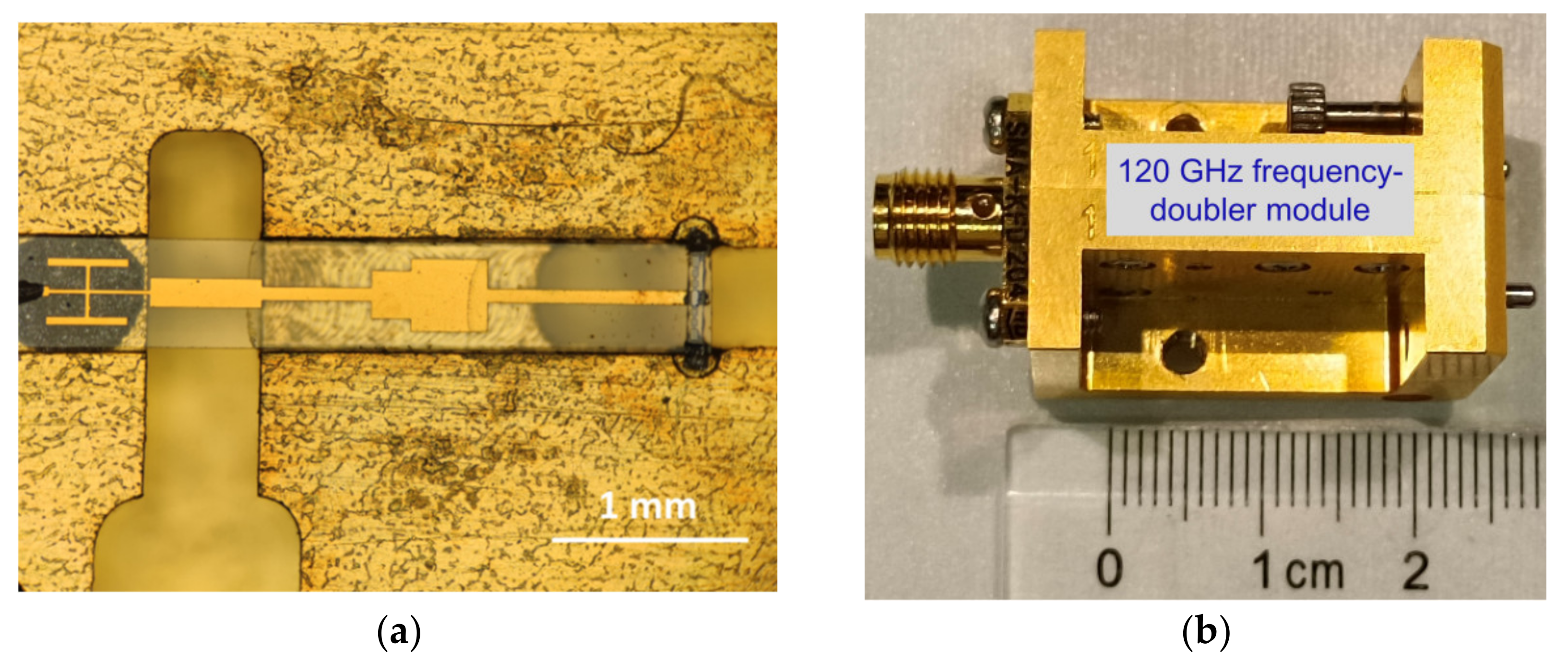
3.2. Fabrication of 120 GHz Frequency Doubler

The fabrication of 120 GHz frequency-doubler module includes the E-plane split-waveguide copper block, waveguide-microstrip structure, and GaN SBD chain. The waveguide-microstrip structure was a deposited 2 μm gold microstrip on 50 μm quartz wafer by electron beam evaporation. The waveguide-microstrip structure was assembled in the E-plane split-waveguide copper block. The GaN SBD chain was assembled on the quartz circuit of output matching by using the conductive adhesive. Assembly details of the 120 GHz frequency-doubler module are shown in Figure 7a. The sub-miniature version A (SMA) coaxial radio frequency (RF) connector and the main transmission circuit were connected by gold wire bonding. Finally, the 120 GHz frequency doubler was fabricated by combining two E-plane split-waveguide copper blocks, as shown in Figure 7b.

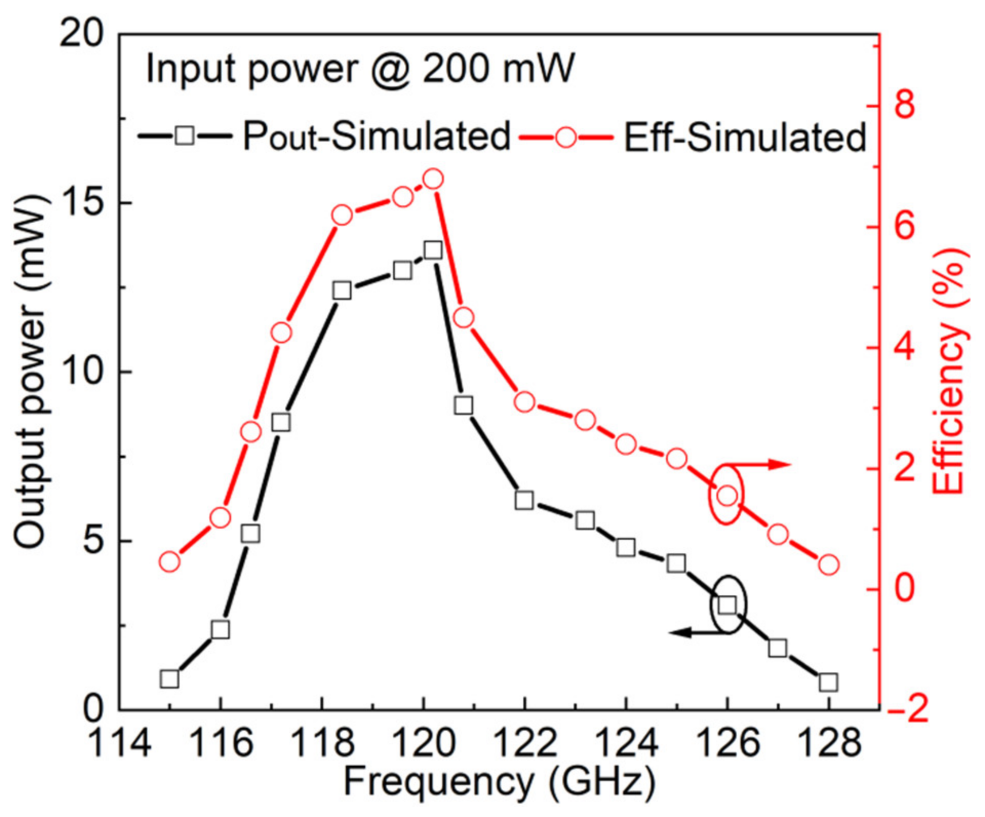
4. Results and Discussion

The input power source of drive 120 GHz frequency-doubler module is a 6× frequency multiplier, which exhibits a input frequency from 50 to 75 GHz. The Agilent analog signal generator E8257D provided the input signal, and the output power of the 120 GHz frequency-doubler module was detected by the PM4 power meter. A voltage of −8.4 V was applied to the anode of the GaN SBD chain by SMA, which can perform a RF swing of high input power and optimal conversion efficiency. A photograph of the test site for the 120 GHz frequency-doubler module is shown in Figure 8.
When driven with 200 mW input power in CW, the output power reached a peak value at 120 GHz, as shown in Figure 9a. There is an agreement between the simulations and measurements for both conversion efficiency and output power, but it is lower than the simulated results. The reason for the difference is mainly due to the loss of the waveguide and assembly error. Figure 9b shows peak output power and conversion efficiency of 120 GHz vs. different input power. The output power of the CW reaches 15.1 mW at 120 GHz with a conversion efficiency of 3%. The lower conversion efficiency is mainly due to the large R s . When the driving power is higher than 0.5 W, the conversion efficiency decreases due to the heat generated and accumulated in the GaN-based SBD chain. The experiments show that the 120 GHz frequency-doubler module can endure an input power of 2 W due to higher breakdown voltage.
Table 2 summarizes the comparison of the key performance between our 120 GHz frequency doubler and other similar solid-state frequency multipliers in a recent report. Compared to GaAs frequency multipliers, the GaN frequency multipliers show much higher power-handling ability. The frequency multipliers of the pulsed output can support higher output power than the CW output due to less heat generation. In the space of waveguide, more anodes can enhance the higher output power. In this work, the 120 GHz frequency doubler generated 15.1 mW CW output power with a conversion efficiency of 3%. By comparing the GaAs-based frequency multiplier (power-handling capability of 0.5 W), our frequency doubler endured an input power of 2 W due to a breakdown voltage of 54.9 V at 1 µA. In addition, GaN SBD on a sapphire substrate has a very low cost compared with GaAs SBD and GaN SBD on SiC.

5. Conclusions

In this work, a solid-state 120 GHz frequency-doubler module of the GaN SBD chain was designed and fabricated with the n/n+-GaN substrate. The GaN SBD chain has a breakdown voltage of 54.9 V at 1 μA, a series resistance of 26.3 Ω, and a cut-off frequency of 587.5 GHz at zero bias. The frequency-doubler module generated 15.1 mW output power at 120 GHz, which was driven with 500 mW input power of the CW. The frequency-doubler module can endure an input power of 2 W due to higher breakdown voltage. Moreover, the temperature distribution of the SBD chain was measured for the first time. The GaN SBD chain works successfully at 337.2 °C. In the following research, we focus on the influencing factor of parasitic resistance and substrate loss, which can improve the conversion efficiency and output power.

Author Contributions

The work presented in this paper was a collaboration of all authors. Experiments and analysis, H.L., J.M., Z.L., C.Y., Y.L. (Yuebo Liu) and H.W.; software, J.M. and D.Z.; resources, Z.W., Y.L. (Yang Liu), X.W., D.Z. and B.Z.; writing—original draft preparation, H.L. and Z.L.; writing—review and editing, H.L., Z.L. and. B.Z.; supervision, X.W., D.Z. and B.Z.; funding acquisition, X.W., D.Z. and B.Z. All authors have read and agreed to the published version of the manuscript.

Funding

This work was supported by Science & Technology Plan of Guangdong Province, China (Grant Nos. 2019B010132003, 2019B010132001), the joint funding of the Nature Science Foundation of China (NSFC) & the Macao Science and Technology Development Fund (FDCT) of China (Grant No. 62061160368), the National Key Research and Development Program (Grant Nos. 2016YFB0400105 and 2017YFB0403001), and the Zhuhai Key Technology Laboratory of Wide Bandgap Semiconductor Power Electronics, Sun Yat-sen University, China.

Institutional Review Board Statement

Not applicable.

Informed Consent Statement

Not applicable.

Data Availability Statement

The data that support the finding of this study are available from the corresponding author upon reasonable request.

Conflicts of Interest

The authors declare no conflict of interest.

References

  1. Mehdi, I.; Siles, J.V.; Lee, C.; Schlecht, E. THz Diode Technology: Status, Prospects, and Applications. Proc. IEEE 2017, 105, 990–1007. [Google Scholar] [CrossRef]
  2. Waters, J.W.; Froidevaux, L.; Harwood, R.S.; Jarnot, R.F.; Pickett, H.M.; Read, W.G.; Siegel, P.H.; Cofield, R.E.; Filipiak, M.J.; Flower, D.A.; et al. The Earth observing system microwave limb sounder (EOS MLS) on the aura Satellite. IEEE Trans. Geosci. Remote. Sens. 2006, 44, 1075–1092. [Google Scholar] [CrossRef]
  3. Choi, J.; Va, V.; Gonzalez-Prelcic, N.; Daniels, R.; Bhat, C.R.; Heath, R.W. Millimeter-Wave Vehicular Communication to Support Massive Automotive Sensing. IEEE Commun. Mag. 2016, 54, 160–167. [Google Scholar] [CrossRef] [Green Version]
  4. Zhang, L.; Karpowicz, N.; Zhang, C.; Zhao, Y.; Zhang, X. Real-time nondestructive imaging with THz waves. Opt. Commun. 2008, 281, 1473–1475. [Google Scholar] [CrossRef]
  5. Hasch, J.; Topak, E.; Schnabel, R.; Zwick, T.; Weigel, R.; Waldschmidt, C. Millimeter-Wave Technology for Automotive Radar Sensors in the 77 GHz Frequency Band. IEEE Trans. Microw. Theory. Tech. 2012, 60, 845–860. [Google Scholar] [CrossRef]
  6. Köhler, R.D.; Tredicucci, A.; Beltram, F.; Beere, H.E.; Linfield, E.H.; Davies, A.G.; Ritchie, D.A.; Iotti, R.C.; Rossi, F. Terahertz semiconductor heterostructure laser. Nature 2002, 417, 156–159. [Google Scholar] [CrossRef] [PubMed]
  7. Williams, B.S. Terahertz quantum-cascade lasers. Nat. Photonics 2007, 1, 517–525. [Google Scholar] [CrossRef] [Green Version]
  8. Maestrini, A.; Mehdi, I.; Siles, J.V.; Ward, J.S.; Lin, R.; Thomas, B.; Lee, C.; Gill, J.; Schlecht, E.; Pearson, J.; et al. Design and Characterization of a Room Temperature All-Solid-State Electronic Source Tunable From 2.48 to 2.75 THz. IEEE Trans. Terahertz Sci. Technol. 2012, 2, 177–185. [Google Scholar] [CrossRef]
  9. Siles, J.V.; Schlecht, E.; Lin, R.; Choonsup, L.; Mehdi, I. High-efficiency planar Schottky diode based submillimeter-wave frequency multipliers optimized for high-power operation. In Proceedings of the 40th International Conference on Infrared, Millimeter, and Terahertz Waves (IRMMW-THz), Hong Kong, China, 23–28 August 2015; p. 1. [Google Scholar]
  10. Cooper, K.B.; Monje, R.R.; Millan, L.; Lebsock, M.; Tanelli, S.; Siles, J.V.; Lee, C.; Brown, A. Atmospheric Humidity Sounding Using Differential Absorption Radar Near 183 GHz. IEEE Geosci. Remote Sens. Lett. 2018, 15, 163–167. [Google Scholar] [CrossRef]
  11. Cojocari, O.; Moro-Melgar, D.; Oprea, I.; Hoefle, M.; Rickes, M. High-Power MM-Wave Sources based on Schottky Diodes. In Proceedings of the 43rd International Conference on Infrared, Millimeter, and Terahertz Waves (IRMMW-THz), Nagoya, Japan, 9–14 September 2018. [Google Scholar]
  12. Schlecht, E.; Chattopadhyay, G.; Maestrini, A.; Pukala, D.; Gill, J.; Martin, S.; Maiwald, F.; Mehdi, I. A high-power wideband cryogenic 200 GHz Schottky ‘substrateless’ multiplier: Modelling design and results. In Proceedings of the Proceedings of 9th International Conference THz Electron, Charlottesville, VA, USA, 5 October 2001; pp. 485–494. [Google Scholar]
  13. Waliwander, T.; Fehilly, M.; O’Brien, E. An Ultra-High Efficiency High Power Schottky Varactor Frequency Doubler to 180–200 GHz. In Proceedings of the Global Symposium on Millimeter Waves (GSMM)/ESA Workshop on Millimetre-Wave Technology and Applications, Espoo, Finland, 6–8 June 2016; pp. 157–160. [Google Scholar]
  14. Chen, Z.; Wang, H.; Alderman, B.; Huggard, P.; Zhang, B.; Fan, Y. 190GHz high power input frequency doubler based on Schottky diodes and AlN substrate. Ieice Electron. Expr. 2016, 13, 20160981. [Google Scholar] [CrossRef] [Green Version]
  15. Mehdi, I.; Maestrini, A.; Pukala, D.; Chattopadhyay, G.; Bruston, J.; Schlecht, E.; Maiwald, F.; Martin, S.; Schlecht, E.; Chattopadhyay, G. Cryogenic Operation of GaAs Based Multiplier Chains to 400 GHz. In Proceedings of the 8th International Conference on Terahertz Electronics, Darmstadt, Germany, 28 September 2000. [Google Scholar]
  16. Cojocari, O.; Moro-Melgar, D.; Oprea, I. High-Power MM-Wave Frequency Multipliers. In Proceedings of the 44th International Conference on Infrared, Millimeter, and Terahertz Waves (IRMMW-THz), Paris, France, 1–6 September 2019. [Google Scholar]
  17. Moro-Melgar, D.; Cojocari, O.; Oprea, I. High Power High Efficiency 270-320 GHz Source Based on Discrete Schottky Diodes. In Proceedings of the 48th European Microwave Conference (EuMC), Madrid, Spain, 26–28 September 2018; pp. 1357–1360. [Google Scholar]
  18. Cojocari, O.; Oprea, I.; Gibson, H.; Walber, A. SubMM-Wave Multipliers by Film-Diode Technology. In Proceedings of the 46th European Microwave Conference (EuMC), London, UK, 4–6 October 2016; pp. 337–340. [Google Scholar]
  19. Montero-de-Paz, J.; Sobornytskyy, M.; Hoefle, M.; Cojocari, O. High Power 150 GHz Schottky based Varactor Doubler. In Proceedings of the Global Symposium on Millimeter Waves (GSMM), Espoo, Finland, 6–8 June 2016; pp. 161–164. [Google Scholar]
  20. Siles, J.V.; Cooper, K.B.; Lee, C.; Lin, R.H.; Chattopadhyay, G.; Mehdi, I. A New Generation of Room-Temperature Frequency-Multiplied Sources With up to 10× Higher Output Power in the 160-GHz-1.6-THz Range. IEEE IEEE Trans. Terahertz Sci. Technol. 2018, 8, 596–604. [Google Scholar] [CrossRef]
  21. Maestrini, A.; Ward, J.S.; Tripon-Canseliet, C.; Gill, J.J.; Lee, C.; Javadi, H.; Attopadhyay, G.C.; Mehdi, I. In-phase power-combined frequency triplers at 300 GHz. IEEE Microw. Wirel. Compon. Lett. 2008, 18, 218–220. [Google Scholar] [CrossRef]
  22. Sites, J.V.; Lee, C.; Lin, R.; Chattopadhyay, G.; Reck, T.; Jung-Kubiak, C.; Mehdi, I.; Cooper, K.B. A High-Power 105-120 GHz Broadband On-Chip Power-Combined Frequency Tripler. IEEE Microw. Wirel. Compon. Lett. 2015, 25, 157–159. [Google Scholar]
  23. Viegas, C.; Liu, H.; Powell, J.; Sanghera, H.; Whimster, A.; Donoghue, L.; Huggard, P.G.; Alderman, B. A 180-GHz Schottky Diode Frequency Doubler with Counter-Rotated E-Fields to Provide In-Phase Power-Combining. IEEE Microw. Wirel. Compon. Lett. 2018, 28, 518–520. [Google Scholar] [CrossRef]
  24. Zhang, B.; Ji, D.; Fang, D.; Liang, S.; Fan, Y.; Chen, X. A Novel 220-GHz GaN Diode On-Chip Tripler with High Driven Power. IEEE Electron Device Lett. 2019, 40, 780–783. [Google Scholar] [CrossRef]
  25. Zhang, L.; Liang, S.; Lv, Y.; Yang, D.; Fu, X.; Song, X.; Gu, G.; Xu, P.; Guo, Y.; Bu, A.; et al. High-Power 300 GHz Solid-State Source Chain Based on GaN Doublers. IEEE Electron Device Lett. 2021, 42, 1588–1591. [Google Scholar] [CrossRef]
  26. Kaganer, V.M.; Brandt, O.; Trampert, A.; Ploog, K.H. X-ray diffraction peak profiles from threading dislocations in GaN epitaxial films. Phys. Rev. B 2005, 72, 045423. [Google Scholar] [CrossRef] [Green Version]
  27. Zhang, B.; Ji, D.; Min, Y.; Fan, Y.; Chen, X. A High-Efficiency 220GHz Doubler Based on the Planar Schottky Varactor Diode. J. of Electron. Mater. 2019, 48, 3603–3611. [Google Scholar] [CrossRef] [Green Version]
  28. Wu, C.; Zhang, Y.; Cui, J.; Li, Y.; Xu, Y.; Xu, R. A 135-190 GHz Broadband Self-Biased Frequency Doubler using Four-Anode Schottky Diodes. Micromachines 2019, 10, 227. [Google Scholar] [CrossRef] [Green Version]
  29. Meng, J.; Qi, L.; Liu, X.; Zhou, J.; Zhang, D.; Jin, Z. The Design of Terahertz Monolithic Integrated Frequency Multipliers Based on Gallium Arsenide Material. Micromachines 2020, 11, 336. [Google Scholar] [CrossRef] [Green Version]
  30. Liang, S.; Song, X.; Zhang, L.; Lv, Y.; Wang, Y.; Wei, B.; Guo, Y.; Gu, G.; Wang, B.; Cai, S.; et al. A 177-183 GHz High-Power GaN-Based Frequency Doubler with Over 200 mW Output Power. IEEE Electron Device Lett. 2020, 41, 669–672. [Google Scholar] [CrossRef]
Figure 1. (a) The 3D structure of the GaN SBD chain. (b) The optical micrograph of the GaN SBD chain. (c) The schematic cross-section of air-bridge SBD with epitaxial information.
Micromachines 13 01172 g001
Figure 2. Characteristics of the fabricated GaN SBD at room temperature and after alloying of 400 °C in O2. (a) Measured C-V curves. (b) Measured I-V curves.
Micromachines 13 01172 g002
Figure 3. Anode of GaN SBD chain temperature distribution at different bias voltages.
Micromachines 13 01172 g003
Figure 4. The overall 3D model of 120 GHz frequency doubler in HFSS. The inset shows the GaN SBD chain in the frequency doubler.
Micromachines 13 01172 g004
Figure 5. Design of the 120 GHz monolithic integrated doubler.
Micromachines 13 01172 g005
Figure 6. Simulated output power and efficiency of 120 GHz frequency doubler at input power of 200 mW.
Micromachines 13 01172 g006
Figure 7. (a) The optical micrograph of 120 GHz frequency doubler imbedded in the split-waveguide block. (b) Overall photograph of the 120 GHz frequency-doubler module.
Micromachines 13 01172 g007
Figure 8. Photograph of test site for the 120 GHz frequency-doubler module.
Micromachines 13 01172 g008
Figure 9. Measurement results of 120 GHz frequency-doubler module. (a) Measured output power and efficiency. (b) Measured output power and efficiency.
Micromachines 13 01172 g009
Table 1. Comparison of main parameters of the GaAs and GaN SBD with one anode.
MaterialsGaAs SBD [27]GaN SBD
Thickness of epitaxial layer (nm)300150
Doping concentration of epitaxial layer (cm3) 2   ×   10−17 4   ×   10−17
Series resistance (Ω)38.8
Zero bias capacitance (fF)4030.3
Barrier voltage (V)0.90.78
Breakdown voltage (V at µA)1018.3
Band gap width (eV)1.423.4
Ideal factor1.21.24
Electron mobility (cm2V1s1)8000900
Table 2. Performance comparison of similar frequency multipliers.
Ref.Diode
Material
Multiplying
Factor
Frequency Band
(GHz)
Input Power
(mW)
Output Power
(mW)
Conversion
Efficiency
Number of
Anodes
[9]GaAs×2170–20050012526%6
[12]GaAs×2184–2121805430%6
[14]GaAs×2190–198260207.7%6
[27]GaAs×2190–2358921.424%6
[28]GaAs×2135–190174137.5%4
[29]GaAs×3210–21830010.53.5%6
[24]GaN×3200–220110017.51.6%8
[30] *GaN×2175–185214024411.4%8
This workGaN×2117–12550015.13%6
* Multipliers of the pulsed output.
Publisher’s Note: MDPI stays neutral with regard to jurisdictional claims in published maps and institutional affiliations.

