
Design, Fabrication, and Dynamic Environmental Test of a Piezoresistive Pressure Sensor

 , , and
Abstract
:1. Introduction
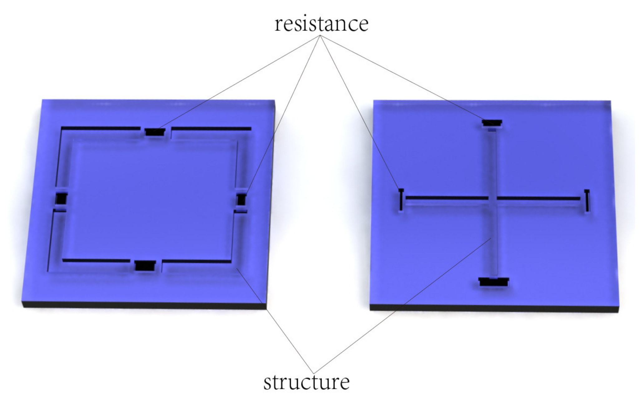
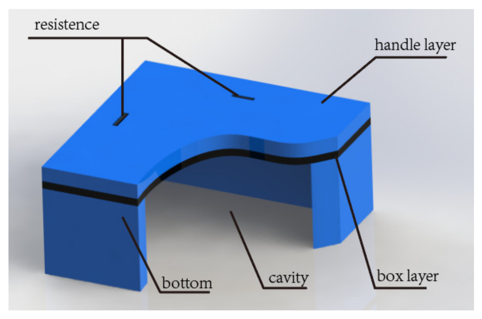
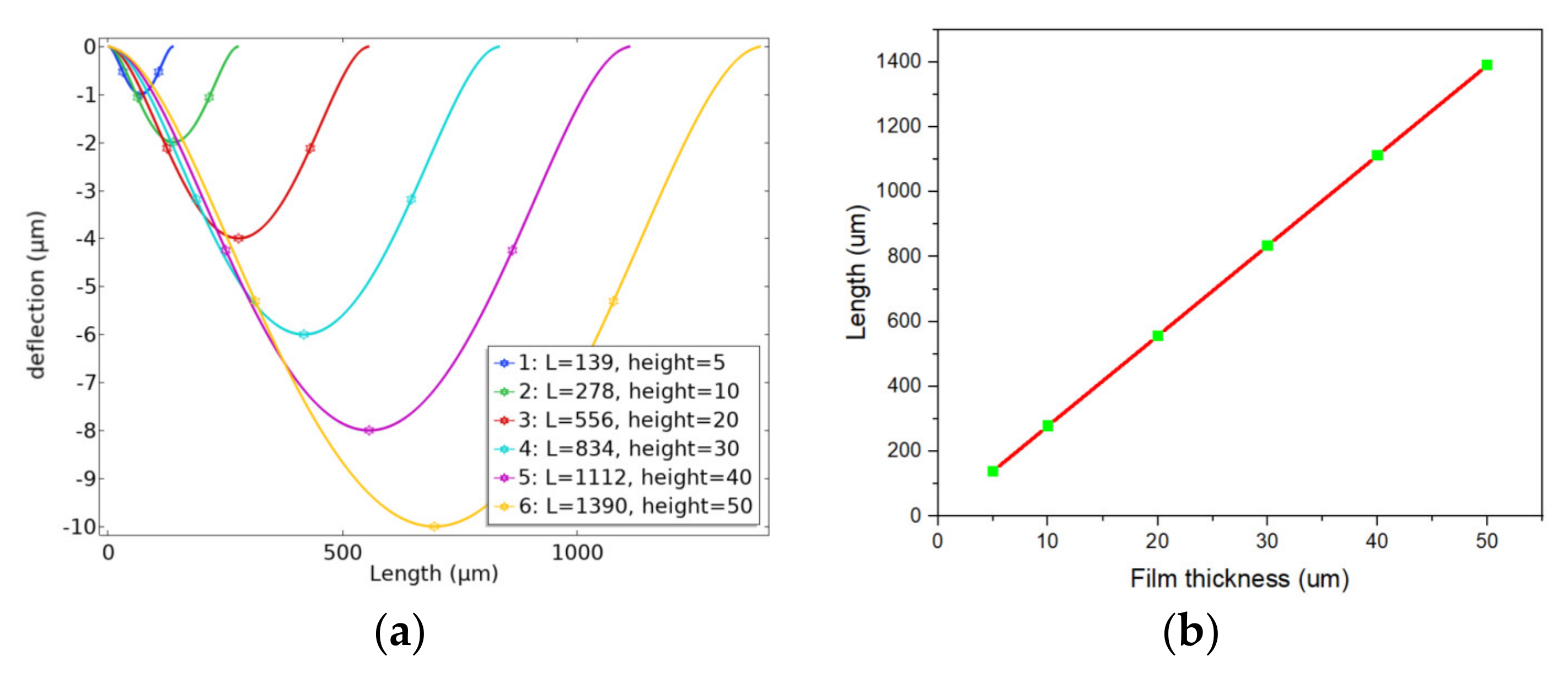
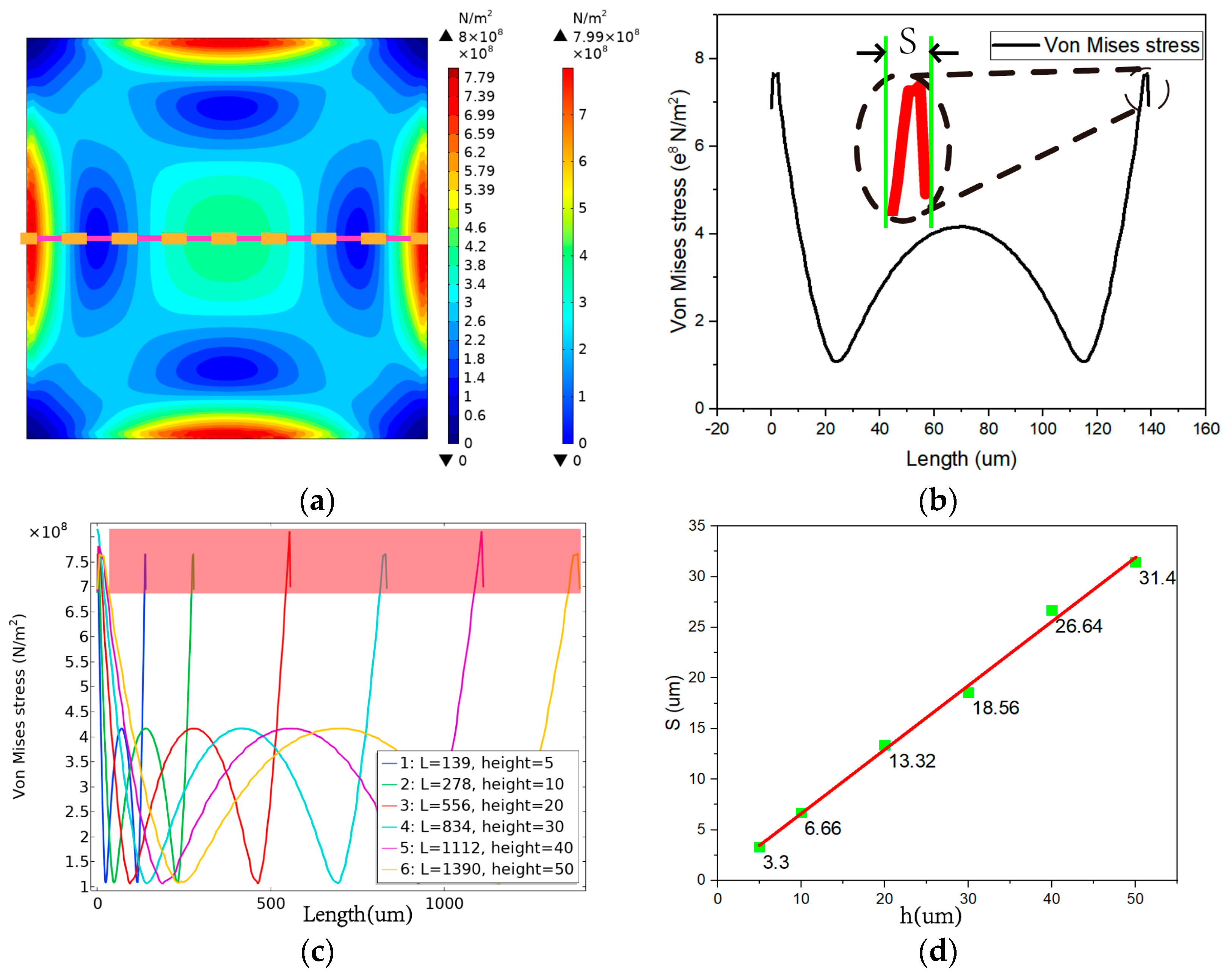
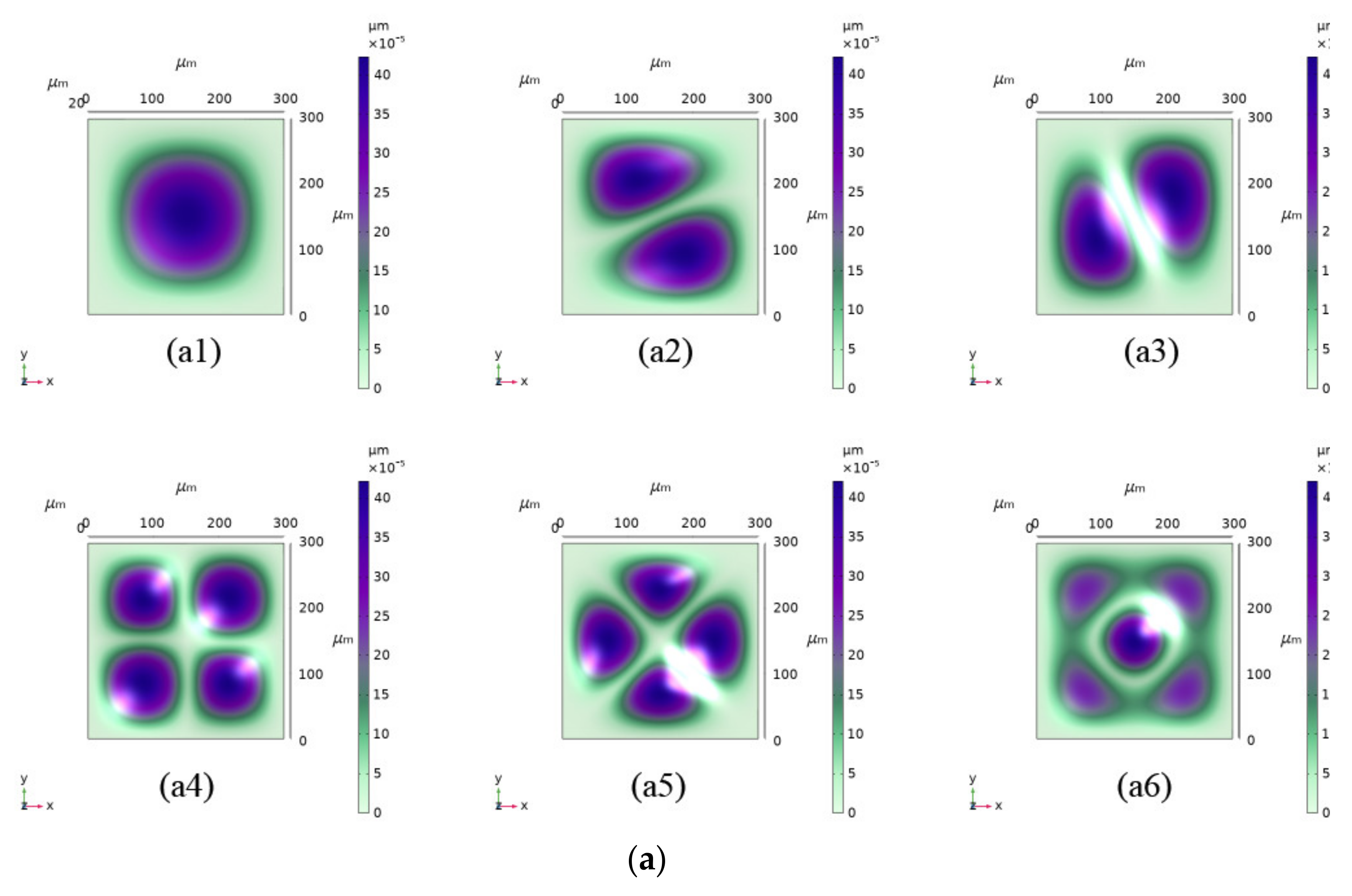
2. Structure Design and Simulation
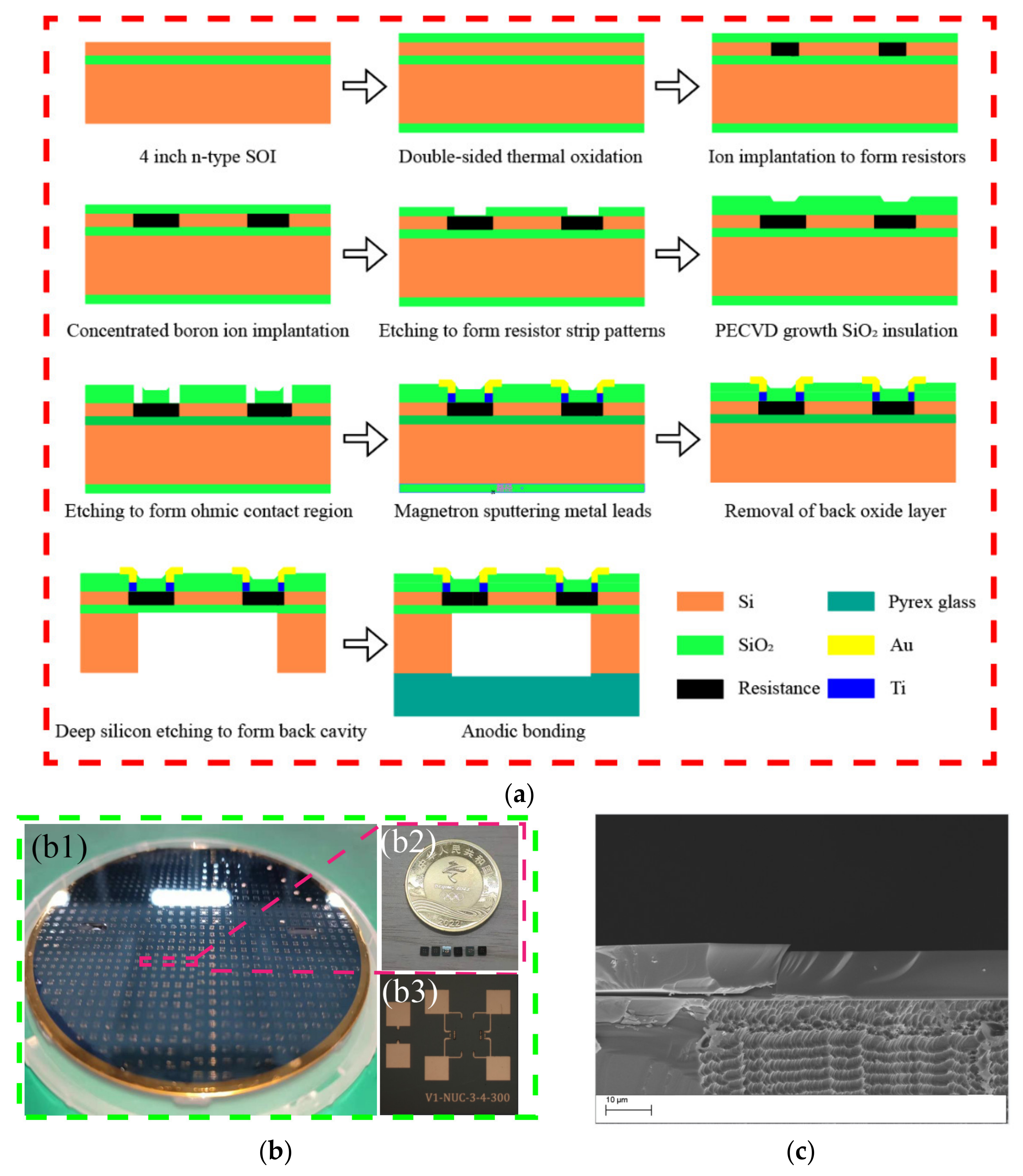
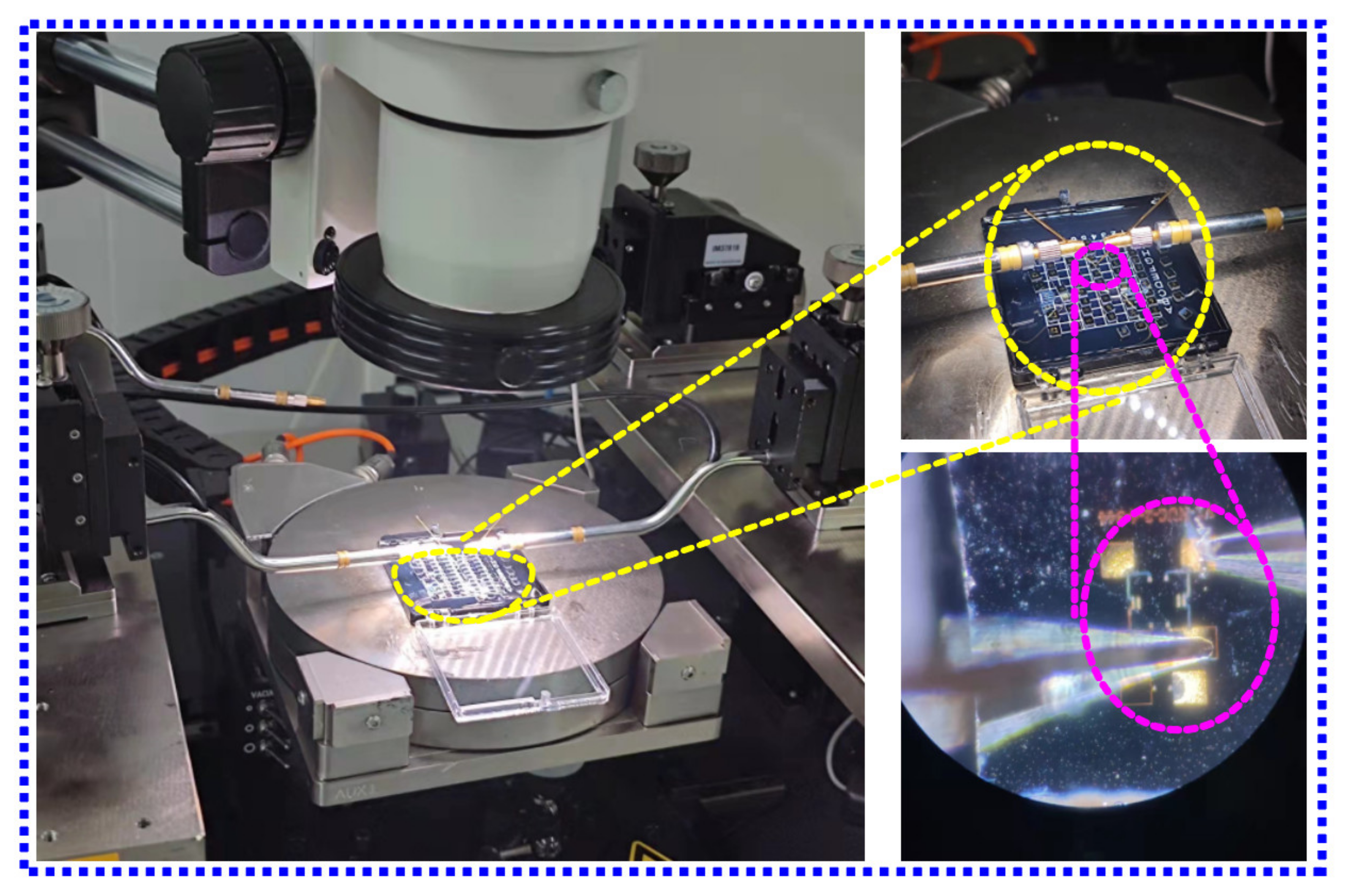
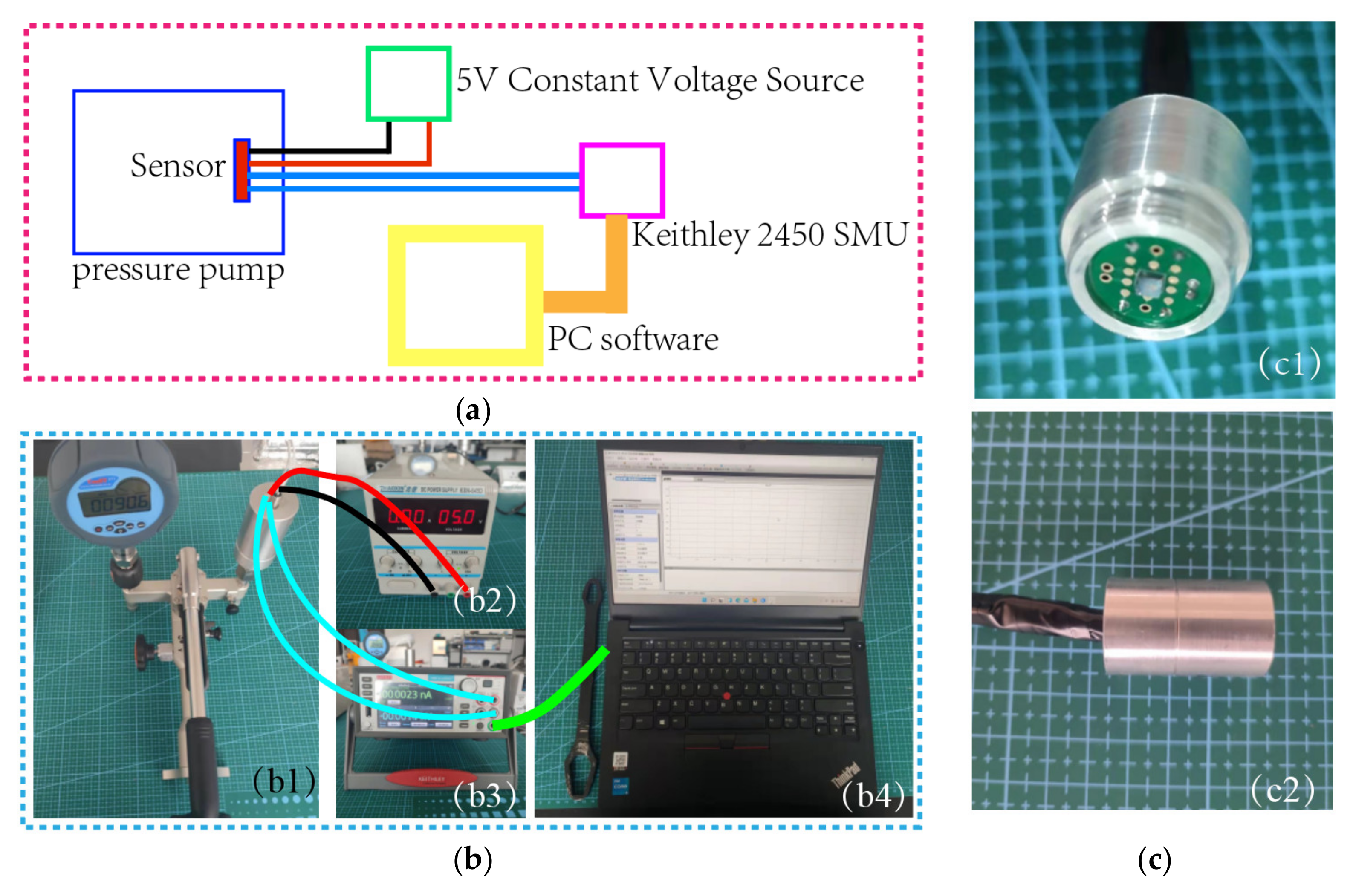
3. Fabrication and Measurement
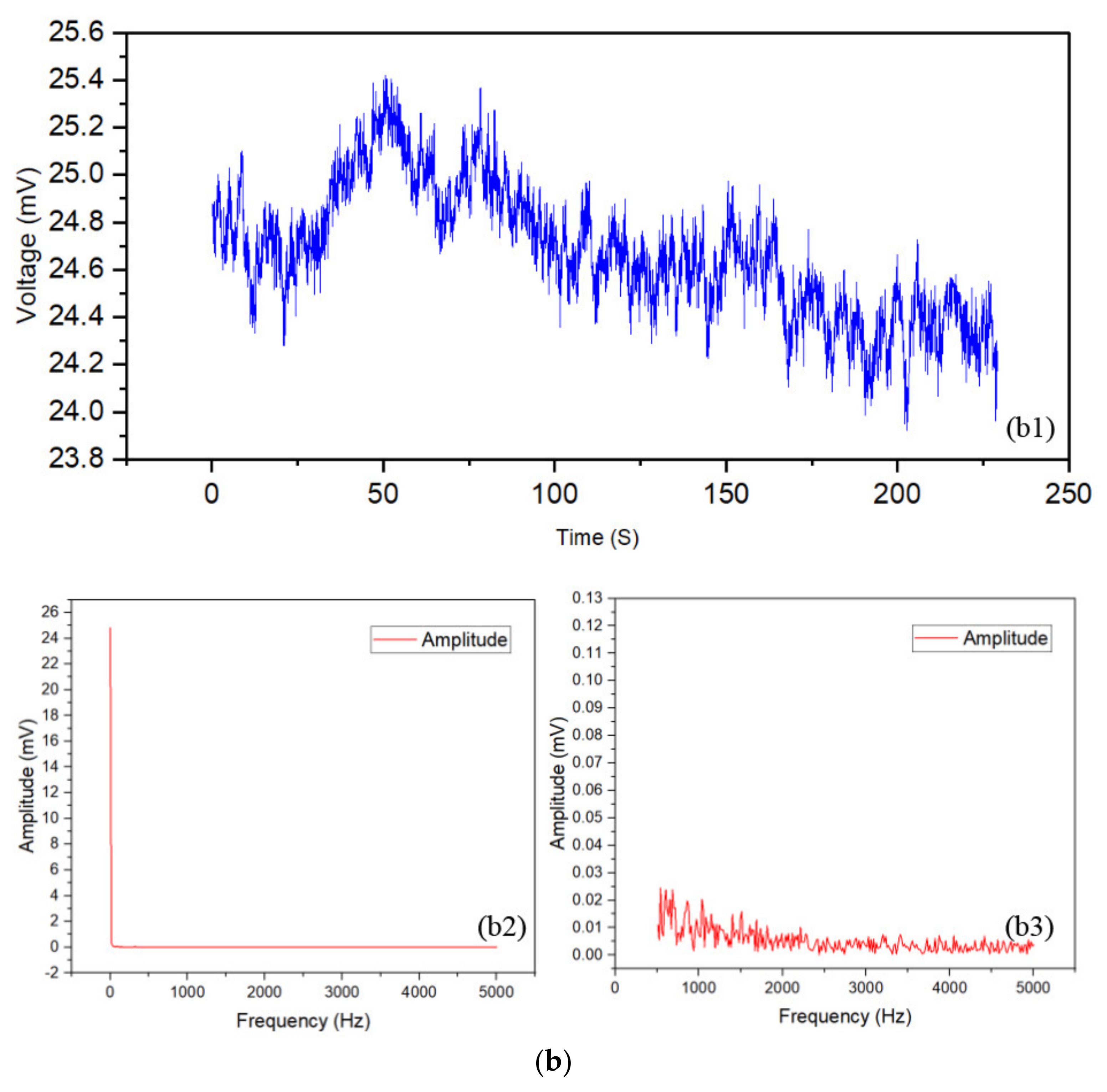
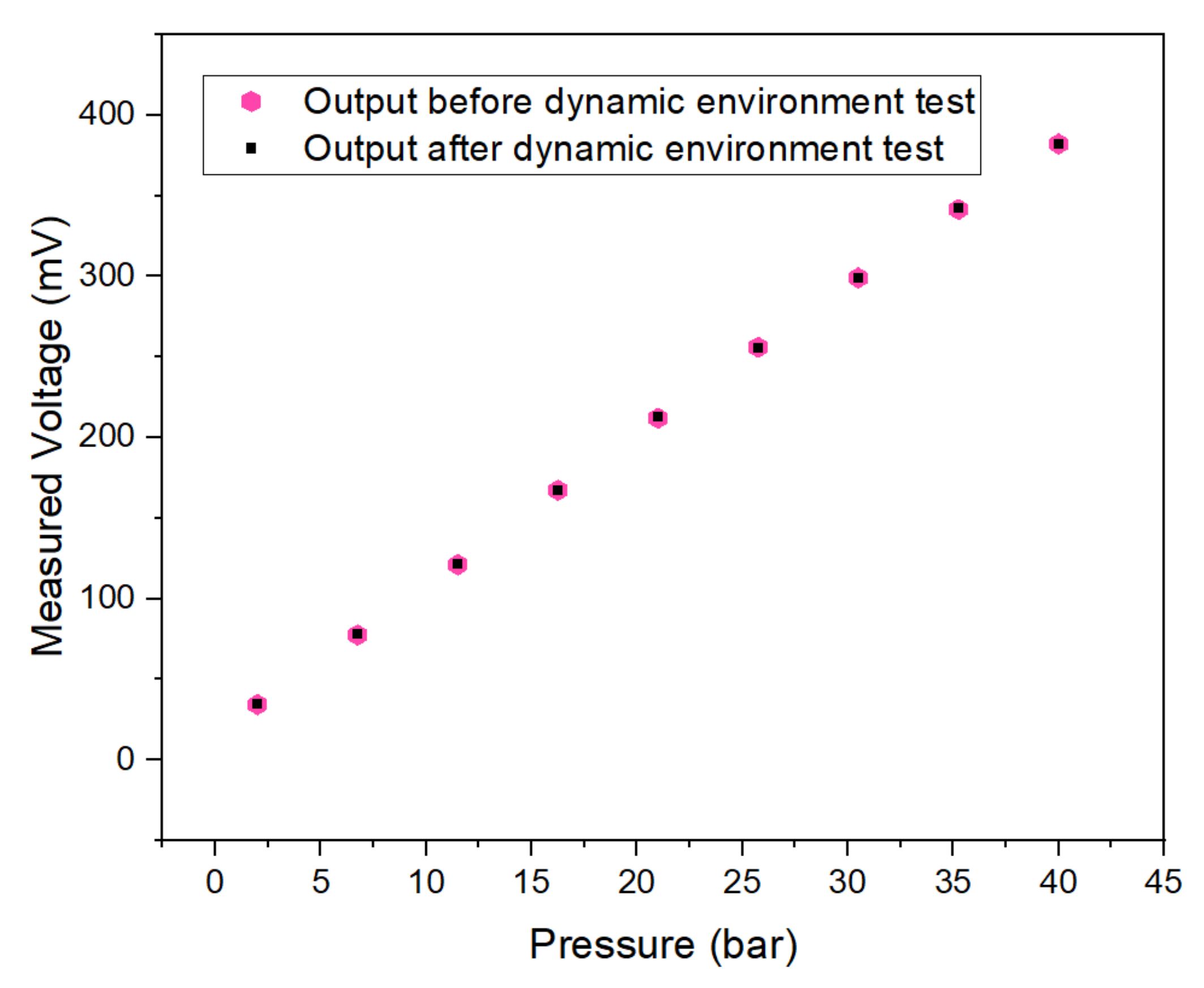
4. Results and Discussion
5. Conclusions
6. Patents
Author Contributions
Funding
Data Availability Statement
Conflicts of Interest
References
- Nguyen, T.; Dinh, T.; Phan, H.P.; Pham, T.A.; Dau, V.T.; Nguyen, N.T.; Dao, D.V. Advances in ultrasensitive piezoresistive sensors: From conventional to flexible and stretchable applications. Mater. Horiz. 2021, 8, 2123–2150. [Google Scholar] [CrossRef] [PubMed]
- Gupta, Y.M. Stress measurements using piezoresistance gauges: Modeling the gauge as an elastic-plastic inclusion. J. Appl. Phys. 1983, 54, 6256–6266. [Google Scholar] [CrossRef]
- Jing, Z.; Zhang, G.Y.; Shi, D.X. Review of graphene-based strain sensors. Chin. Phys. B 2013, 22, 35–43. [Google Scholar]
- Cranny, A.; Cotton, D.; Chappell, P.H.; Beeby, S.P.; White, N.M. Thick-film force and slip sensors for a prosthetic hand. Sens. Actuators A Phys. 2005, 123–124, 162–171. [Google Scholar] [CrossRef] [Green Version]
- Zhou, C.; Zang, J.; Xue, C.; Ma, Y.; Hua, X.; Gao, R.; Zhang, Z.; Li, B.; Zhang, Z. Design of a Novel Medical Acoustic Sensor Based on MEMS Bionic Fish Ear Structure. Micromachines 2022, 13, 163. [Google Scholar] [CrossRef]
- Lipomi, D.J.; Vosgueritchian, M.; Tee, B.C.; Hellstrom, S.L.; Lee, J.A.; Fox, C.H.; Bao, Z. Skin-like pressure and strain sensors based on transparent elastic films of carbon nanotubes. Nat. Nanotechnol. 2011, 6, 788–792. [Google Scholar] [CrossRef]
- Amjadi, M.; Kyung, K.U.; Park, I.; Sitti, M. Stretchable, Skin-Mountable, and Wearable Strain Sensors and Their Potential Applications: A Review. Adv. Funct. Mater. 2016, 26, 1678–1698. [Google Scholar] [CrossRef]
- Gao, L.; Wang, Y.; Hu, X.; Zhou, W.; Lu, Y. Cellular Carbon-Film-Based Flexible Sensor and Waterproof Supercapacitors. ACS Appl. Mater. Interfaces 2019, 11, 26288–26297. [Google Scholar] [CrossRef]
- Balderrama, V.S.; Leon-Gil, J.A.; Fernández-Benavides, D.A.; Ponce-Hernández, J.; Bandala-Sánchez, M. MEMS Piezoresistive Pressure Sensor Based on Flexible PET Thin-Film for Applications in Gaseous-Environments. IEEE Sens. J. 2022, 22, 1939–1947. [Google Scholar] [CrossRef]
- Meena, K.V.; Sankar, A.R. Biomedical catheters with integrated miniature piezoresistive pressure sensors: A Review. IEEE Sens. J. 2021, 21, 10241–10290. [Google Scholar] [CrossRef]
- Kumar, K.S.; Xu, Z.; Kalairaj, M.S.; Ponraj, G.; Huang, H.; Ng, C.-F.; Wu, Q.H.; Ren, H. Stretchable Capacitive Pressure Sensing Sleeve Deployable onto Catheter Balloons towards Continuous Intra-Abdominal Pressure Monitoring. Biosensors 2021, 11, 156. [Google Scholar] [CrossRef] [PubMed]
- Zhong, G.-Y.; Liu, Y.; Song, J.; Zhao, Q.; Li, Y.-S.; Li, F.-Y. Strong piezoresistance effect of small molecule organic semiconductors. J. Phys. D-Appl. Phys. 2008, 41, 205106. [Google Scholar] [CrossRef]
- Komati, B.; Agnus, J.L.; Clévy, C.; Lutz, P. Prototyping of a highly performant and integrated piezoresistive force sensor for microscale applications. J. Micromech. Microeng. 2014, 24, 035018. [Google Scholar] [CrossRef] [Green Version]
- Li, S.; Liang, T.; Wang, W.; Hong, Y.; Zheng, T. A novel SOI pressure sensor for high temperature application. J. Semicond. 2015, 36, 014014. [Google Scholar] [CrossRef]
- Barlian, A.A.; Park, W.-T.; Mallon, J.R., Jr.; Rastegar, A.J.; Pruitt, B.L. Review: Semiconductor Piezoresistance for Microsystems. Proc. IEEE 2009, 97, 513–552. [Google Scholar] [CrossRef] [Green Version]
- Phan, H.-P.; Dao, D.V.; Nakamura, K.; Dimitrijev, S.; Nguyen, N.-T. The Piezoresistive Effect of SiC for MEMS Sensors at High Temperatures: A Review. J. Microelectromech. Syst. 2015, 24, 1663–1677. [Google Scholar] [CrossRef] [Green Version]
- Medjahdi, N.; Benmoussa, N.; Benyoucef, B. Modeling, Simulation and Optimization of the Mechanical Response of Micromechanical Silicon Cantilever: Application to Piezoresistive Force Sensor. Phys. Procedia 2014, 55, 348–355. [Google Scholar] [CrossRef] [Green Version]
- Pramanik, C.; Saha, H. Piezoresistive pressure sensing by porous silicon membrane. IEEE Sens. J. 2006, 6, 301–309. [Google Scholar] [CrossRef]
- Wang, W.; He, H.; Bian, Y.; Yang, Y. A MEMS High Temperature Pressure Sensor. Micronanoelectron. Technol. 2016, 53, 387–393. [Google Scholar] [CrossRef]
- Shimazoe, M.; Matsuoka, Y.; Yasukawa, A.; Tanabe, M. A Special Silicon Diaphragm Pressure Sensor with High Output and High-Accuracy. Sens. Actuators 1982, 2, 275–282. [Google Scholar] [CrossRef]
- Kinnell, P.K.; King, J.; Lester, M.; Craddock, R. A Hollow Stiffening Structure for Low Pressure Sensors. In Proceedings of the 23rd Eurosensors Conference, Lausanne, Switzerland, 6–9 September 2009. [Google Scholar]
- Zhang, S.; Wang, T.; Lou, L.; Tsang, W.M.; Sawada, R.; Kwong, D.-L.; Lee, C. Annularly Grooved Diaphragm Pressure Sensor with Embedded Silicon Nanowires for Low Pressure Application. J. Microelectromech. Syst. 2014, 23, 1396–1407. [Google Scholar] [CrossRef]
- Huang, X.; Zhang, D. A high sensitivity and high linearity pressure sensor based on a peninsula-structured diaphragm for low-pressure ranges. Sens. Actuators A-Phys. 2014, 216, 176–189. [Google Scholar] [CrossRef]
- Kumar, S.S.; Pant, B.D. Fabrication and characterization of pressure sensor, and enhancement of output characteristics by modification of operating pressure range. In Proceedings of the 2015 19th International Symposium on VLSI Design and Test (VDAT), Ahmedabad, India, 26–29 June 2015. [Google Scholar]
- Kumar, S.; Pant, B. Design of piezoresistive MEMS absolute pressure sensor. In Proceedings of the 16th International Workshop on Physics of Semiconductor Devices in Kanpur, India, Kanpur, India, 14–17 December 2012; SPIE: Bellingham, WA, USA; pp. 308–317. [Google Scholar]
- Leondes, C.T. MEMSNEMS: Handbook Techniques and Applications; Springer: New York, NY, USA, 2006. [Google Scholar]
- Elgamel, H.E. Closed-form expressions for the relationships between stress, diaphragm deflection, and resistance change with pressure in silicon piezoresistive pressure sensors. Sens. Actuators A Phys. 1995, 50, 17–22. [Google Scholar] [CrossRef]
- Zhang, Z.; Liu, G.; Wang, K. Fabrication of Needle-Like Silicon Nanowires by Using a Nanoparticles-Assisted Bosch Process for Both High Hydrophobicity and Anti-Reflection. Micromachines 2021, 12, 1009. [Google Scholar] [CrossRef] [PubMed]
- Knowles, K.M.; van Helvoort, A.T.J. Anodic bonding. Int. Mater. Rev. 2006, 51, 273–311. [Google Scholar] [CrossRef]
- Nag, M.; Singh, J.; Kumar, A.; Alvi, P.A.; Singh, K. Sensitivity enhancement and temperature compatibility of graphene piezoresistive MEMS pressure sensor. Microsyst. Technol. -Micro-Nanosyst. -Inf. Storage Processing Syst. 2019, 25, 3977–3982. [Google Scholar] [CrossRef]
- Zheng, P.; Rougieux, F.E.; Macdonald, D.; Cuevas, A. Measurement and Parameterization of Carrier Mobility Sum in Silicon as a Function of Doping, Temperature and Injection Level. IEEE J. Photovolt. 2014, 4, 560–565. [Google Scholar] [CrossRef] [Green Version]
- Castro, H.F.; Correia, V.; Pereira, N.; Costab, P.; Oliveiraa, J.; Lanceros-Mendez, S. Printed Wheatstone bridge with embedded polymer based piezoresistive sensors for strain sensing applications. Addit. Manuf. 2018, 20, 119–125. [Google Scholar] [CrossRef]
- Anh Vang, T.; Zhang, X.; Zhu, B. Effects of Temperature and Residual Stresses on the Output Characteristics of a Piezoresistive Pressure Sensor. IEEE Access 2019, 7, 27668–27676. [Google Scholar] [CrossRef]
- Tian, B.; Shang, H.; Wang, W. Research on Temperature Zero Drift of SiC Piezoresistive Pressure Sensor Based on Asymmetric Wheatstone Bridge. Silicon 2021, 14, 5445–5451. [Google Scholar] [CrossRef]
- Hsueh, C.H.; Luttrell, C.R.; Cui, T. Thermal stress analyses of multilayered films on substrates and cantilever beams for micro sensors and actuators. J. Micromech. Microeng. 2006, 16, 2509–2515. [Google Scholar] [CrossRef]
- Bower, A.F. Applied Mechanics of Solids; CRC Press: Boca Raton, FL, USA, 2009. [Google Scholar]
- Lin, H.-C.; Ye, Y.-C. Reviews of bearing vibration measurement using fast Fourier transform and enhanced fast Fourier transform algorithms. Adv. Mech. Eng. 2019, 11, 1–12. [Google Scholar] [CrossRef]


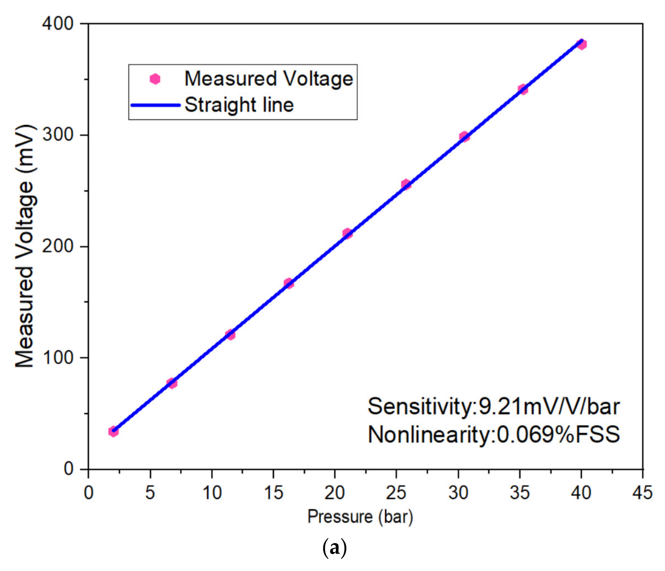
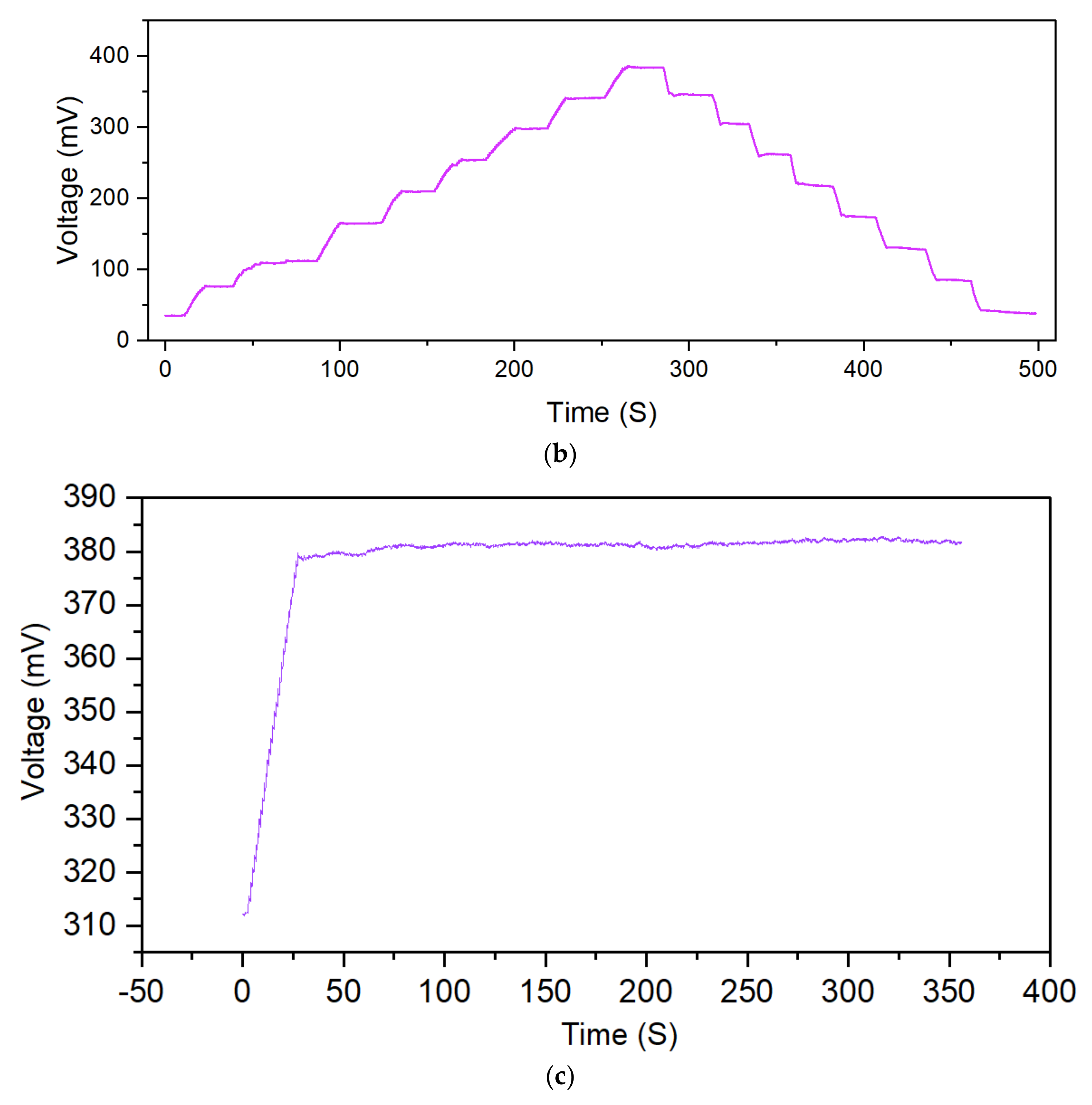
| Sensor | Sensitivity (mV/V/bar) | Pressure Nonlinearity (%FSS) | Full Range Pressure |
|---|---|---|---|
| Proposed sensor | 9.21 | 0.069% | 40 bar |
| Sensor in [24] | 6.03 | 3.89% | 30 bar |
| Sensor in [24] | 6.58 | 0.33% | 10 bar |
| Sensor in [25] | 5.18 | 0.02% | 30 bar |
| Sensor in [25] | 3.69 | 0.011% | 30 bar |
| Parameter | Diaphragm Length | Diaphragm Thickness | Resistor Length | Resistor Width | Cavity Height | Chip Size |
|---|---|---|---|---|---|---|
| Value (µm) | 306 | 11 | 80 | 8 | 389 | 2500*2500 |
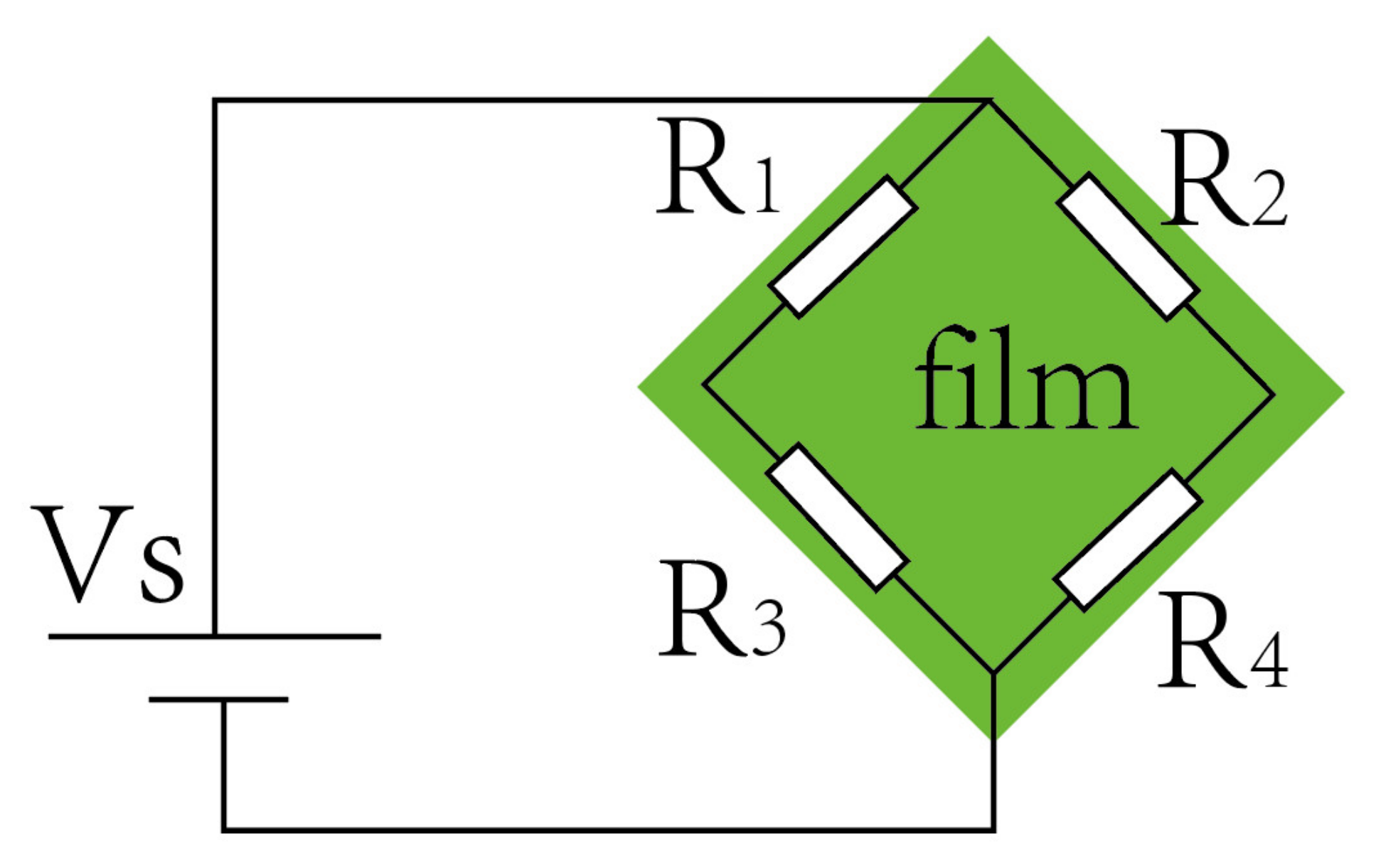
| Parameter | Value | Parameter | Value |
|---|---|---|---|
| Resistance (kΩ) | 1.9 | Nonlinearity (%FSS) | 0.069 |
| Zero output (mV) | 16.5 | TCS (%FSS/°C) | −0.030 |
| Sensitivity (mV/V/bar) | 9.21 | Full-range time drift (mV/V/min) | 0.553 |
| Repeatability (%FSS) | 0.49 | Hysteresis (%FSS) | 2.6 |
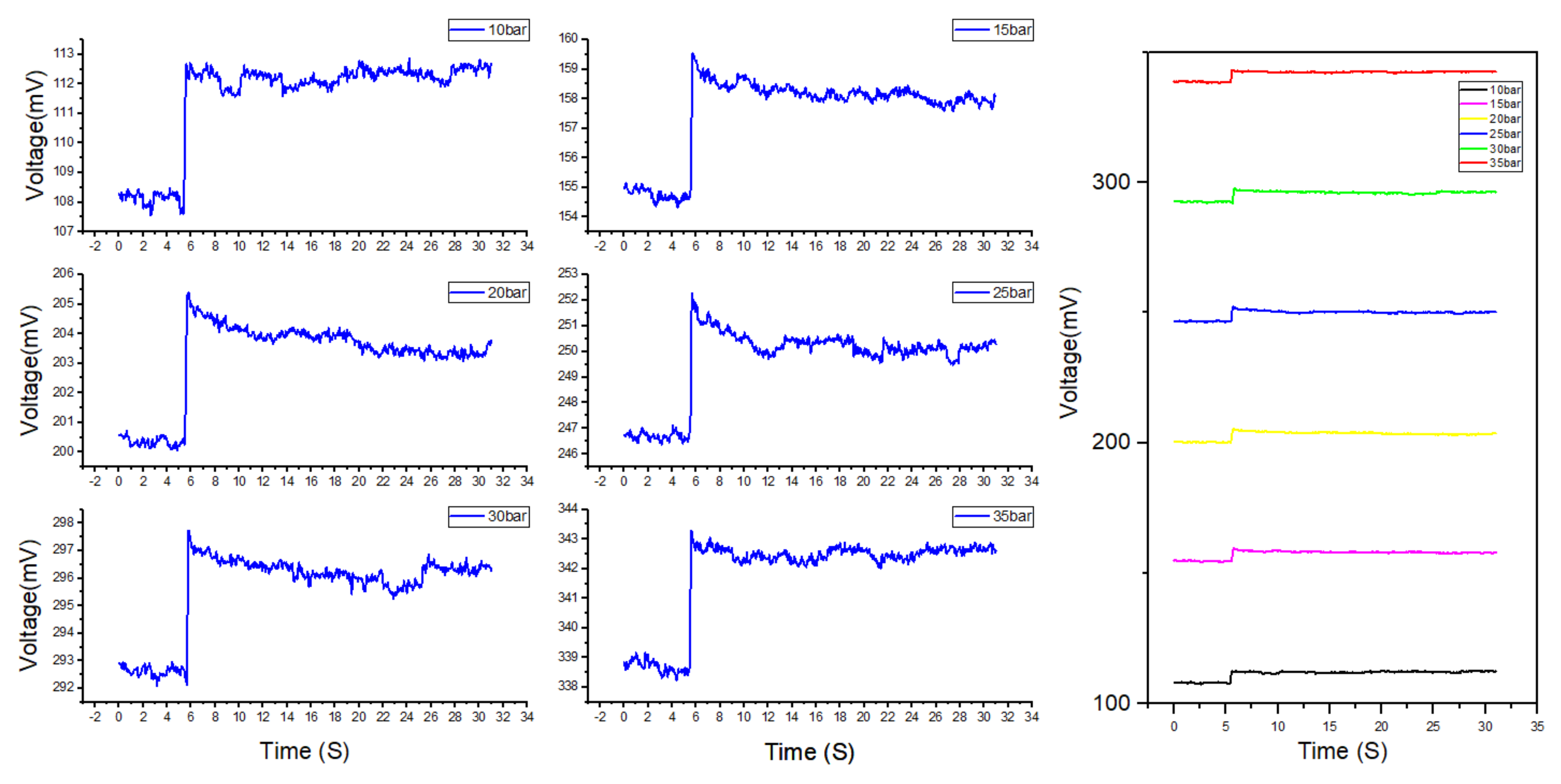
| Pressure/bar | 10 | 15 | 20 | 25 | 30 | 35 |
|---|---|---|---|---|---|---|
| Average voltage (mV) | 112.25 | 158.21 | 203.80 | 250.30 | 296.27 | 342.51 |
| Peak voltage (mV) | 112.87 | 159.55 | 205.39 | 252.27 | 297.74 | 343.29 |
| ΔPeak voltage (mV) | 0.611 | 1.340 | 1.590 | 1.968 | 1.470 | 0.771 |
Publisher’s Note: MDPI stays neutral with regard to jurisdictional claims in published maps and institutional affiliations. |
© 2022 by the authors. Licensee MDPI, Basel, Switzerland. This article is an open access article distributed under the terms and conditions of the Creative Commons Attribution (CC BY) license (https://creativecommons.org/licenses/by/4.0/).
Share and Cite
Gao, R.; Zhang, W.; Jing, J.; Liao, Z.; Zhao, Z.; Yao, B.; Zhang, H.; Guo, Y.; Xu, Y.; Wang, Y.; et al. Design, Fabrication, and Dynamic Environmental Test of a Piezoresistive Pressure Sensor. Micromachines 2022, 13, 1142. https://doi.org/10.3390/mi13071142
Gao R, Zhang W, Jing J, Liao Z, Zhao Z, Yao B, Zhang H, Guo Y, Xu Y, Wang Y, et al. Design, Fabrication, and Dynamic Environmental Test of a Piezoresistive Pressure Sensor. Micromachines. 2022; 13(7):1142. https://doi.org/10.3390/mi13071142
Chicago/Turabian StyleGao, Rui, Wenjun Zhang, Junmin Jing, Zhiwei Liao, Zhou Zhao, Bin Yao, Huiyu Zhang, Yuzhen Guo, Yanbo Xu, Yonghua Wang, and et al. 2022. "Design, Fabrication, and Dynamic Environmental Test of a Piezoresistive Pressure Sensor" Micromachines 13, no. 7: 1142. https://doi.org/10.3390/mi13071142