
Effect of Grain Structure and Ni/Au-UBM Layer on Electromigration-Induced Failure Mechanism in Sn-3.0Ag-0.5Cu Solder Joints


Abstract
:1. Introduction
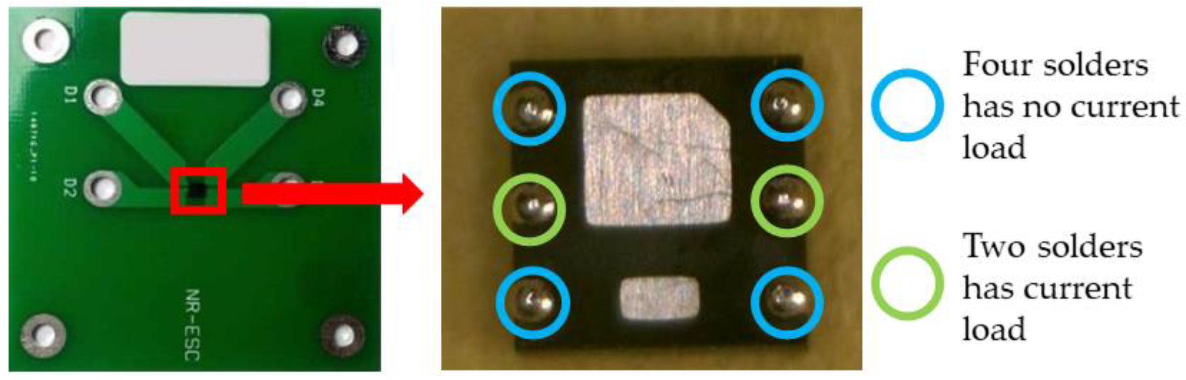
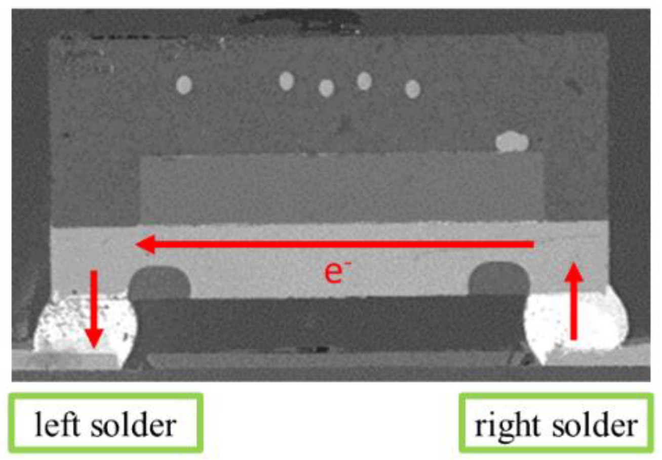
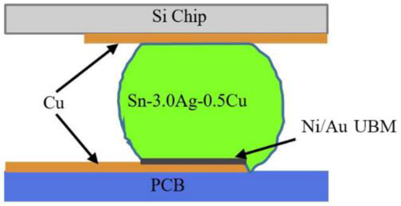
2. Experimental Procedures
3. Results and Discussion
4. Conclusions
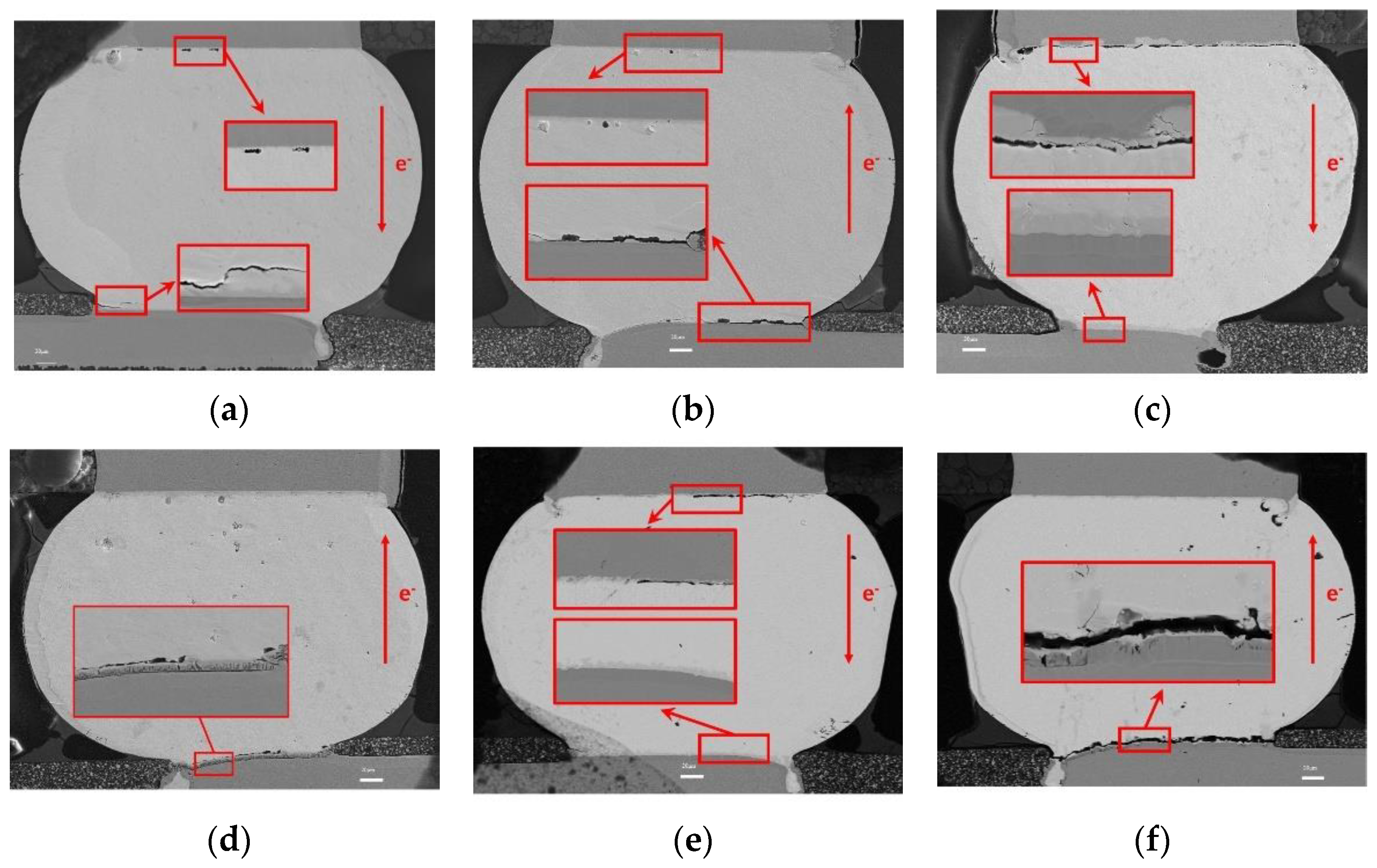
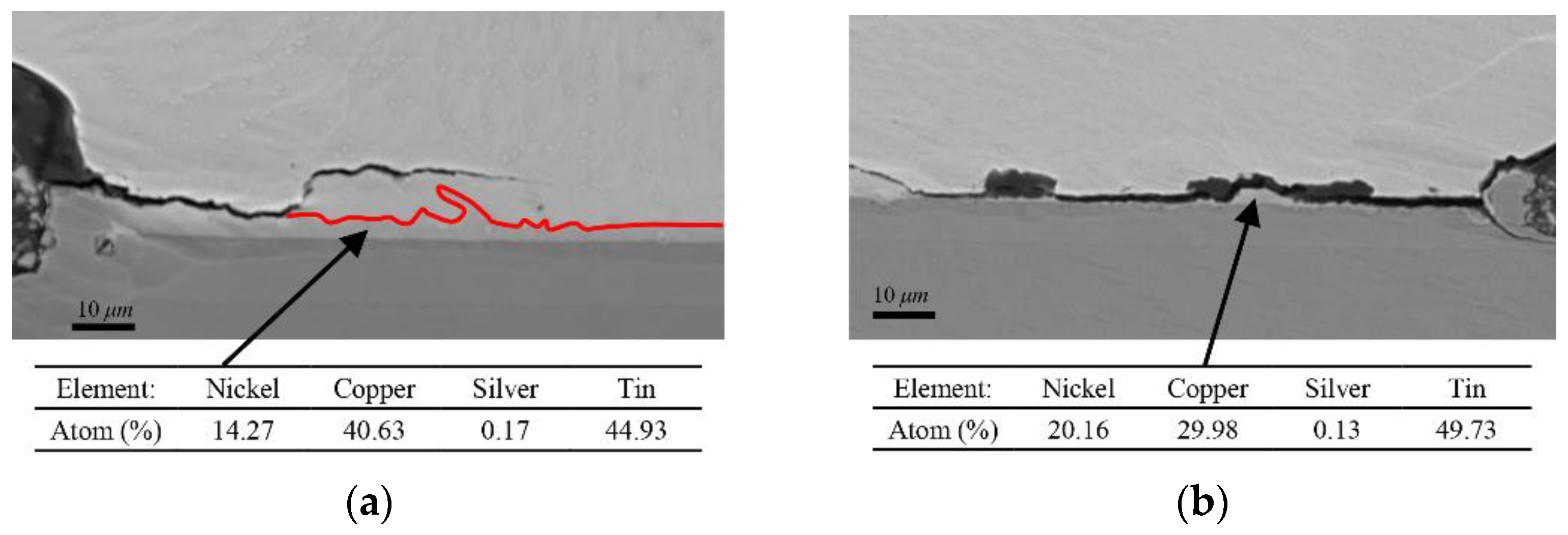
- Both Ni/Au-UBM layer and grain structure would affect the EM-induced failure. Voids or cracks are evident at the cathode end in soler bumps during EM, but there is no significant consumption of Cu pad because of the Ni/Au-UBM layer. The presence of Ni/Au-UBM layer on the Cu pad can inhibit atoms diffused between solder bump and Cu pad, and cracks at the interface near Cu pad induced failure that would occur during EM.
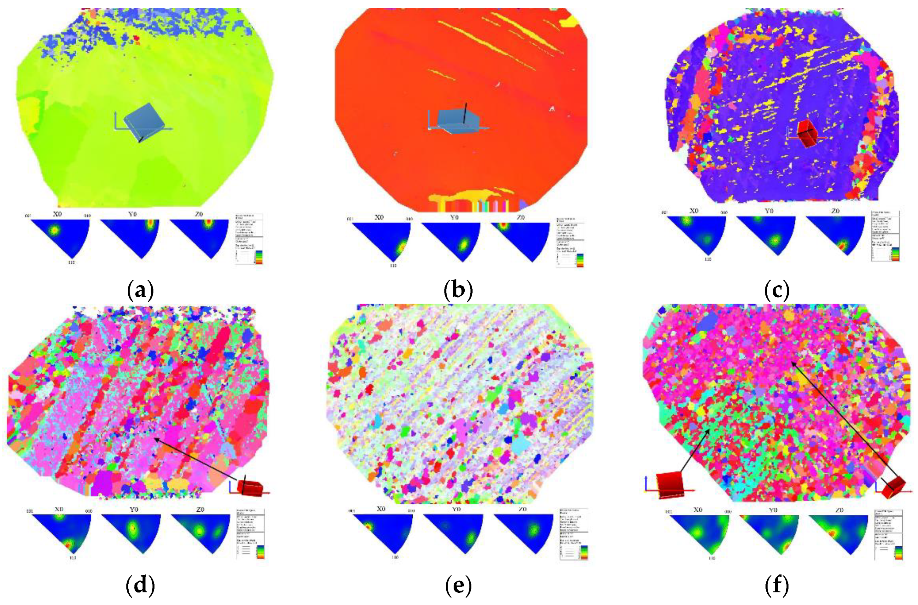
- The EM lifetime of single crystal solder bumps is lower than that of polycrystalline solder bumps when the c-axis of single crystal solder bumps is perpendicular to the electron flow direction. Moreover, the single crystal structure increased the brittleness of the solder bump, and cracks are easily generated and expanded under the stress caused by the mismatch of thermal expansion coefficients between the solder bump and IMC near Cu pad.
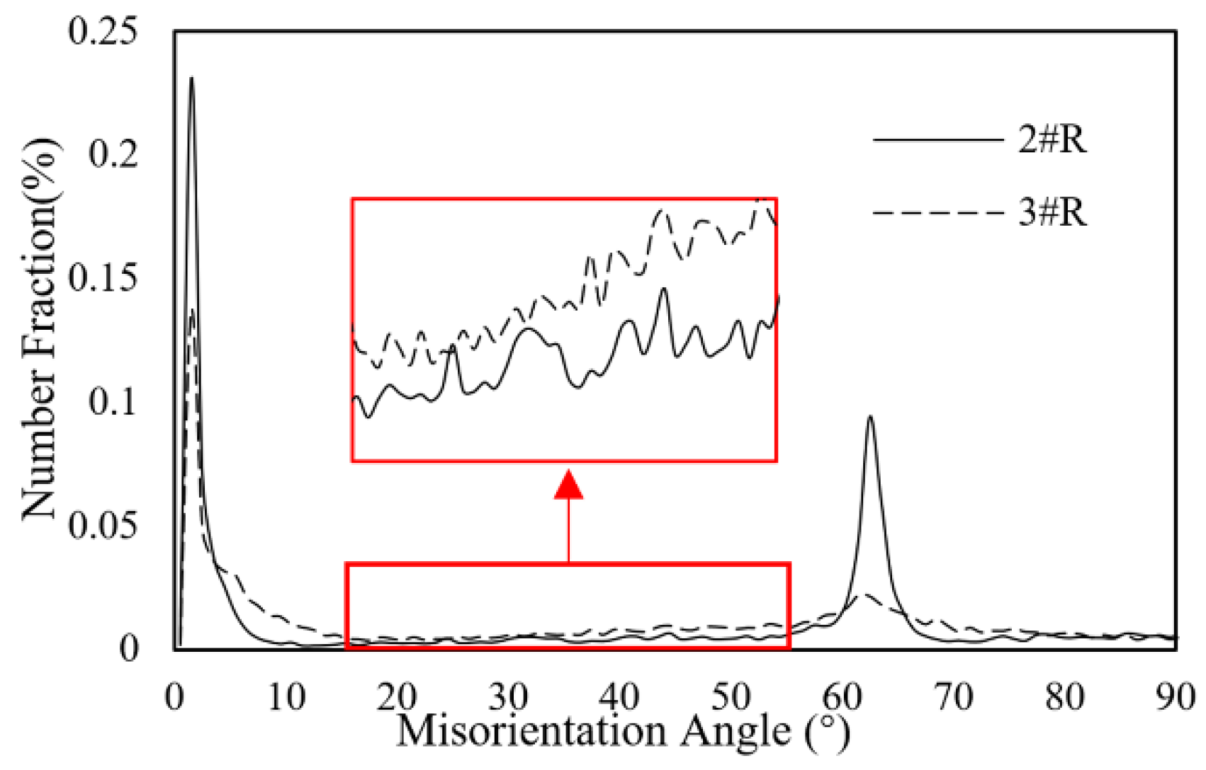
- From the statistical results on the misorientation angle distribution in polycrystalline solder bumps, the electromigration-induced failure will be more likely to occur when the misorientation angles are in the range of 15–55°, which is consistent with the previous literature.
Author Contributions
Funding
Institutional Review Board Statement
Informed Consent Statement
Data Availability Statement
Conflicts of Interest
References
- Tu, K.N. Reliability challenges in 3D IC packaging technology. Microelectron. Reliab. 2011, 51, 517–523. [Google Scholar] [CrossRef]
- Ceric, H.; Selberherr, S. Electromigration in submicron interconnect features of integrated circuits. Mater. Sci. Eng. R Rep. 2010, 71, 53–86. [Google Scholar] [CrossRef]
- Jiang, Y.M.; Li, H.L.; Chen, G.; Mei, Y.H.; Wang, M.Y. Electromigration behavior of Cu/Sn3.0Ag0.5Cu/Cu ball grid array solder joints. J. Mater. Sci. Mater. Electron. 2019, 30, 6224–6233. [Google Scholar] [CrossRef]
- Liu, Y.; Liang, L.; Irving, S.; Luk, T. 3D Modeling of electromigration combined with thermal–mechanical effect for IC device and package. Microelectron. Reliab. 2008, 48, 811–824. [Google Scholar] [CrossRef]
- Dandu, P.; Fan, X.J.; Liu, Y.; Diao, C. Finite element modeling on electromigration of solder joints in wafer level packages. Microelectron. Reliab. 2010, 50, 547–555. [Google Scholar] [CrossRef]
- Lu, M.; Shih, D.; Lauro, P.; Goldsmith, C.; Henderson, D.W. Effect of Sn grain orientation on electromigration degradation mechanism in high Sn-based Pb-free solders. Appl. Phys. Lett. 2008, 92, 211909. [Google Scholar] [CrossRef]
- Tseng, H.W.; Lu, C.T.; Hsiao, Y.H.; Liao, P.L.; Chuang, Y.C.; Chung, T.Y.; Liu, C.Y. Electromigration-induced failures at Cu/Sn/Cu flip-chip joint interfaces. Microelectron. Reliab. 2010, 50, 1159–1162. [Google Scholar] [CrossRef]
- Lee, K.; Kim, K.S.; Tsukada, Y.; Suganuma, K.; Yamanaka, K.; Kuritani, S.; Ueshima, M. Influence of crystallographic orientation of Sn-Ag-Cu on electromigration in flip-chip joint. Microelectron. Reliab. 2011, 51, 2290–2297. [Google Scholar] [CrossRef]
- Chen, J.; Guo, J.; Liu, K.; Shang, J. Dependence of electromigration damage on Sn grain orientation in Sn-Ag-Cu solder joints. J. Appl. Phys. Lett. 2013, 114, 153509. [Google Scholar] [CrossRef] [Green Version]
- Chen, J.; Xu, M.; Jin, Y.; Wang, K.; Chun, Y.; Lu, H. Effect of electric field and Sn grain orientation on Cu consumption in Sn/Cu solder joint. Comp. Mater. Sci. 2014, 95, 166–171. [Google Scholar] [CrossRef]
- Ho, C.E.; Yang, C.H.; Hsu, L.H. Electromigration in thin-film solder joints. Surf. Coat. Technol. 2014, 259, 257–261. [Google Scholar] [CrossRef]
- Tian, Y.; Han, J.; Guo, F. Effects of β-Sn grain c-axis on electromigration behavior in BGA Sn3.0Ag0.5Cu solder interconnects. J. Mater. Sci. Mater. Electron. 2017, 28, 10785–10793. [Google Scholar] [CrossRef]
- Ni, J.; Ring, M.; Hao, J.; Liu, Y.; Maniatty, A.M. Modeling effect of grain orientation on degradation in tin-based solder—Part II: Electromigration experiments. IEEE Trans. Compon. Pack. Manuf. Technol. 2019, 9, 1993–1999. [Google Scholar] [CrossRef]
- Fu, X.; Liu, M.; Xu, K.; Chen, S.; Shi, Y.; Fu, Z.; Huang, Y.; Chen, H.; Yao, R. The in-situ observation of grain rotation and microstructure evolution induced by electromigration in Sn-3.0Ag-0.5Cu solder joints. Materials 2020, 13, 5497. [Google Scholar] [CrossRef] [PubMed]
- Huang, M.L.; Zhao, J.F.; Zhang, Z.J.; Zhao, N. Dominant effect of high anisotropy in β-Sn grain on electromigration-induced failure mechanism in Sn-3.0Ag-0.5Cu interconnect. J. Alloys Compd. 2016, 678, 370–374. [Google Scholar] [CrossRef]
- Shen, Y.; Chen, C. Effect of Sn grain orientation on formation of Cu6Sn5 intermetallic compounds during electromigration. Scripta Mater. 2017, 128, 6–9. [Google Scholar] [CrossRef]
- Lee, T.Y.; Tu, K.N.; Frear, D.R. Electromigration of eutectic SnPb and SnAg3.8Cu0.7 flip chip solder bumps and under-bump metallization. J. Appl. Phys. 2001, 90, 4502–4508. [Google Scholar] [CrossRef]
- Yu, D.; Wu, C.; He, D.; Zhao, N.; Wang, L.; Lai, J. Effects of Cu contents in Sn-Cu solder on the composition and morphology of intermetallic compounds at a solder/Ni interface. J. Mater. Sci. 2005, 20, 2205–2212. [Google Scholar] [CrossRef]
- Zeng, G.; Xue, S.; Zhang, L.; Gao, L.; Dai, W.; Luo, J. A review on the interfacial intermetallic compounds between Sn-Ag-Cu based solders and substrates. J. Mater. Sci. Mater. Electron. 2010, 21, 421–440. [Google Scholar] [CrossRef]
- Zhang, Y.; Liang, L.; Zhu, D. The effects of grain structure on electromigration failure of the lead-free solder bump. Int. J. Eng. Model. 2018, 31, 79–93. [Google Scholar]
- Ni, J. Modeling Microstructure Effects on Electromigration in Tin-Based Solder Bumps. Ph.D. Thesis, Rensselaer Polytechnic Institute, Troy, MI, USA, 2017. [Google Scholar]
- Liang, L.; Zhang, Y.; Liu, Y. Prediction of electromigration failure of solder joints and its sensitivity analysis. J. Electron. Packag. 2011, 133, 031002. [Google Scholar] [CrossRef]
- Mrowec, S. Defects and Diffusion in Solids; Elsevier: Amsterdam, The Netherlands, 1980; p. 466. [Google Scholar]


| Sample | EM Lifetime/h | EM Treatment Time/h |
|---|---|---|
| 1# | 43.5 | 100 |
| 2# | 86.6 | 200 |
| 3# | 78.5 | 200 |
Publisher’s Note: MDPI stays neutral with regard to jurisdictional claims in published maps and institutional affiliations. |
© 2022 by the authors. Licensee MDPI, Basel, Switzerland. This article is an open access article distributed under the terms and conditions of the Creative Commons Attribution (CC BY) license (https://creativecommons.org/licenses/by/4.0/).
Share and Cite
Zhang, Y.; Zhang, J.; Wang, Y.; Fang, Y. Effect of Grain Structure and Ni/Au-UBM Layer on Electromigration-Induced Failure Mechanism in Sn-3.0Ag-0.5Cu Solder Joints. Micromachines 2022, 13, 953. https://doi.org/10.3390/mi13060953
Zhang Y, Zhang J, Wang Y, Fang Y. Effect of Grain Structure and Ni/Au-UBM Layer on Electromigration-Induced Failure Mechanism in Sn-3.0Ag-0.5Cu Solder Joints. Micromachines. 2022; 13(6):953. https://doi.org/10.3390/mi13060953
Chicago/Turabian StyleZhang, Yuanxiang, Jicheng Zhang, Yong Wang, and Yike Fang. 2022. "Effect of Grain Structure and Ni/Au-UBM Layer on Electromigration-Induced Failure Mechanism in Sn-3.0Ag-0.5Cu Solder Joints" Micromachines 13, no. 6: 953. https://doi.org/10.3390/mi13060953