
Investigation of Negative Bias Temperature Instability Effect in Nano PDSOI PMOSFET


Abstract
:1. Introduction
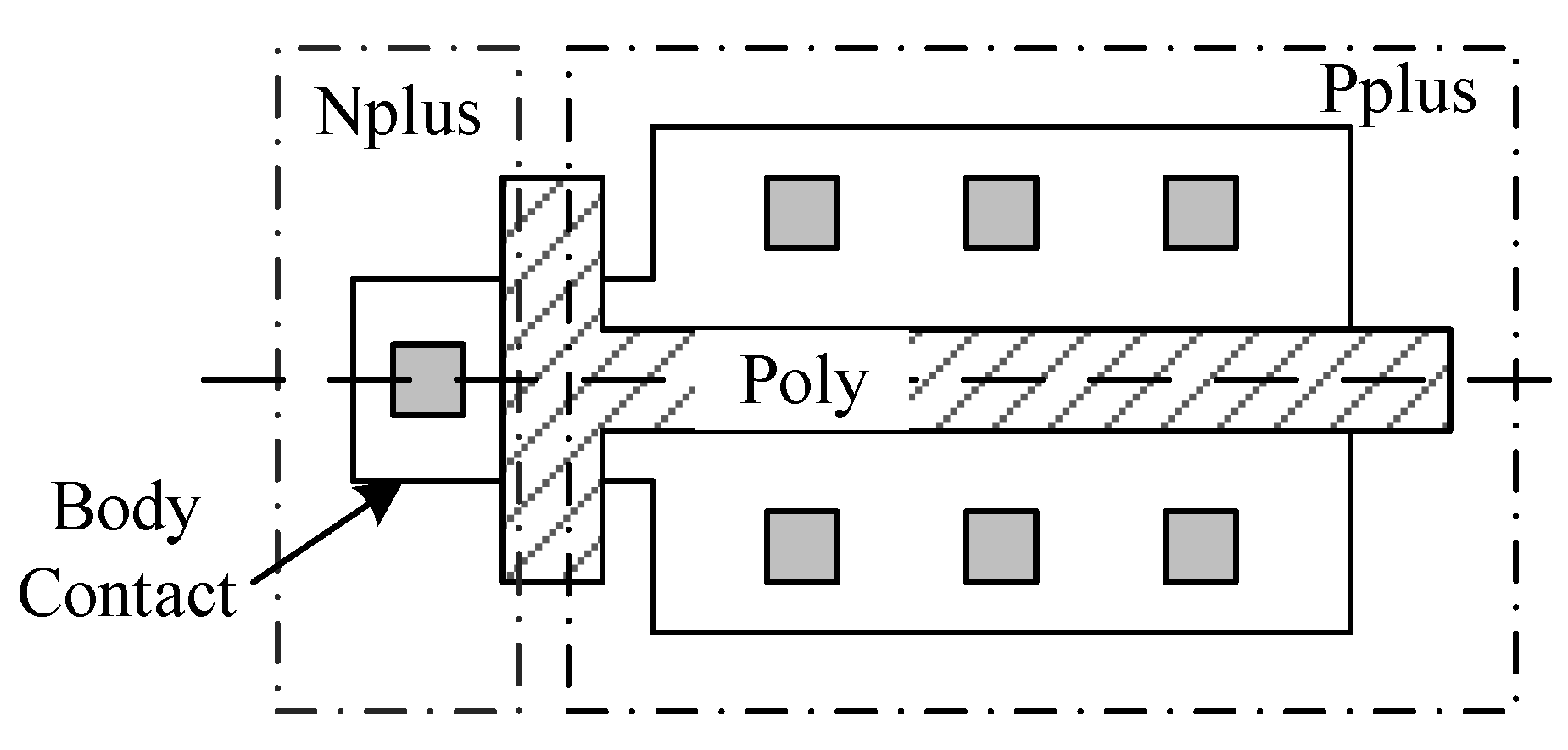
2. Materials and Methods
3. Results and Discussion
3.1. NBTI Degradation of I–V Characteristic
3.2. Construction of NBTI Lifetime Prediction Model
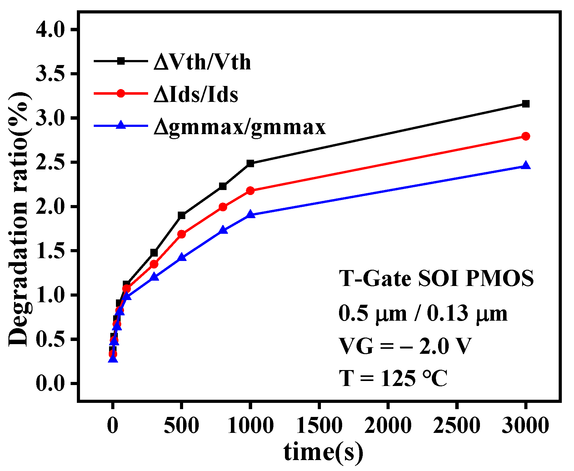
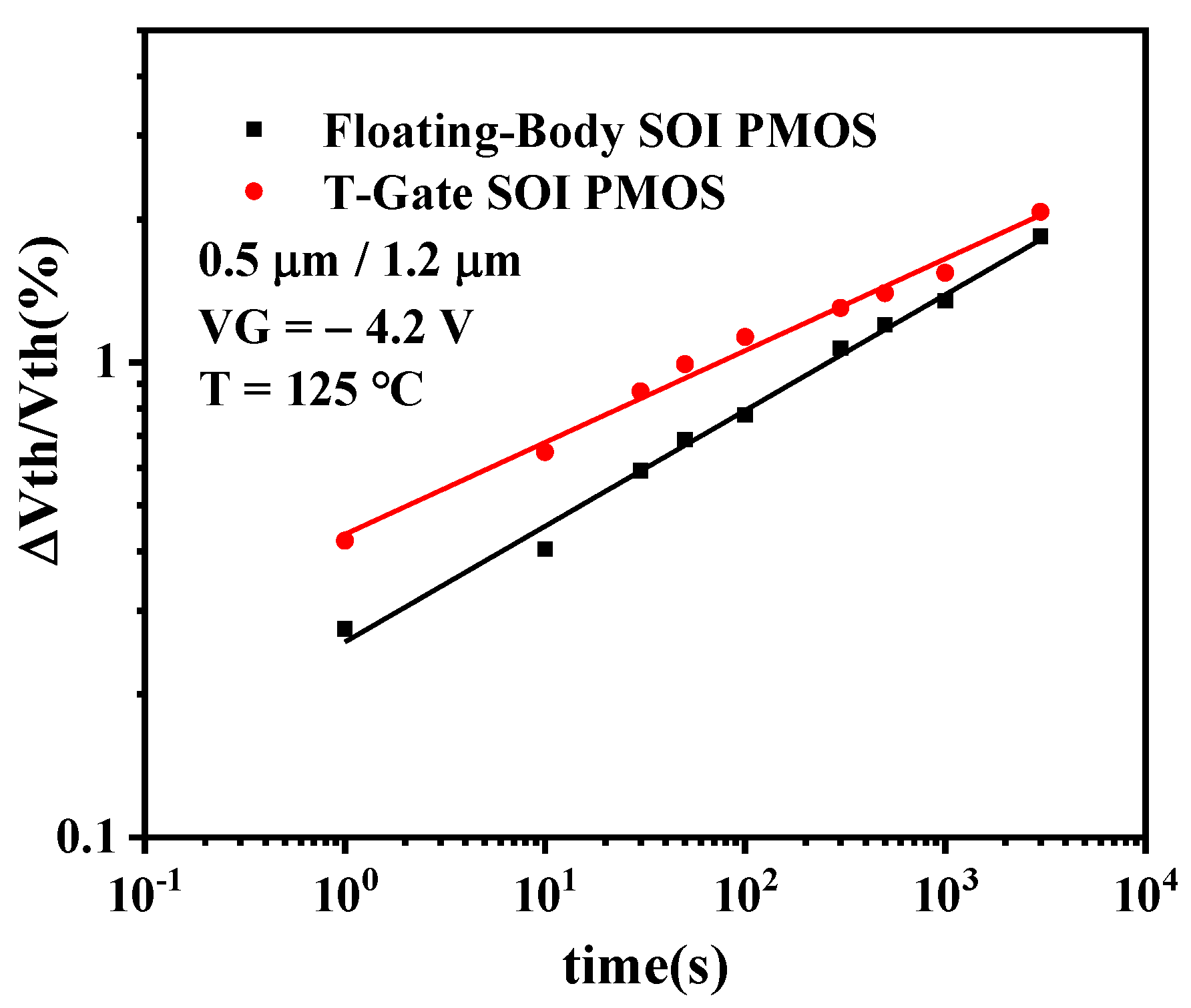
3.2.1. Stress Time Dependence of NBTI Degradation
3.2.2. Gate Bias Dependence of NBTI Degradation
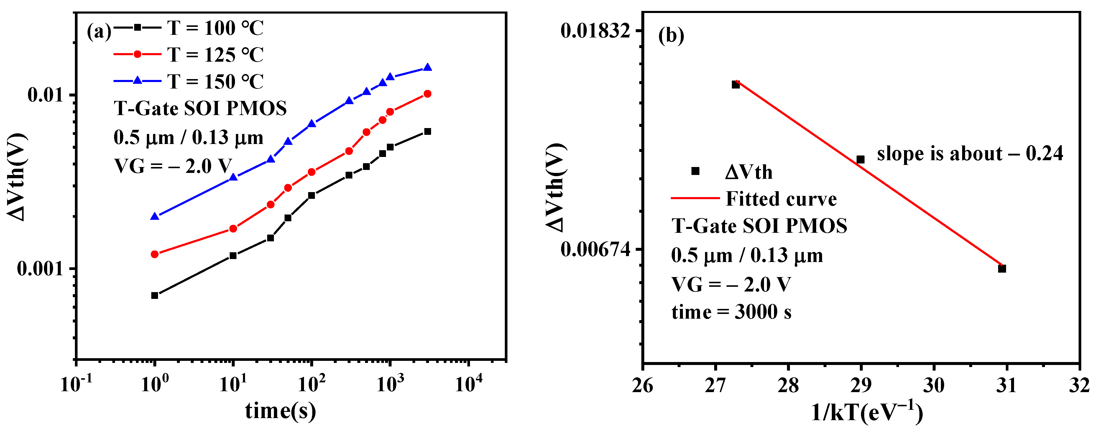
3.2.3. Temperature Dependence of NBTI Degradation
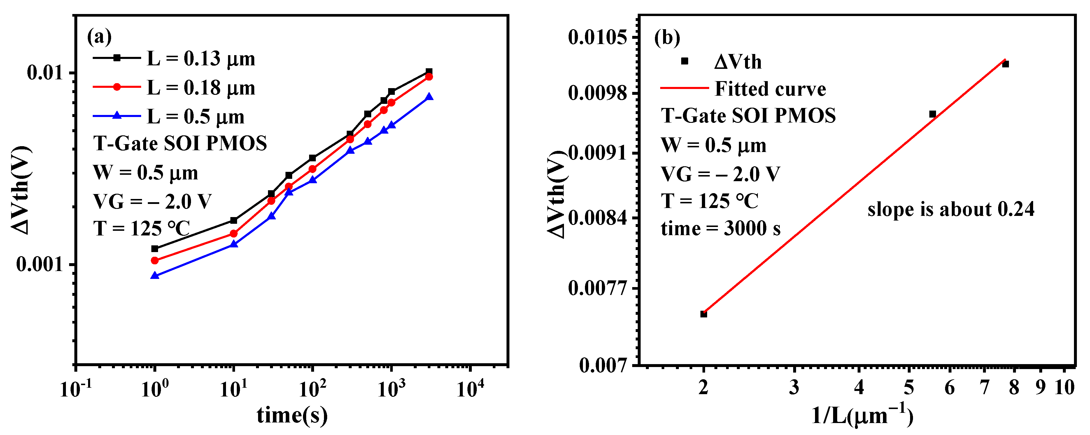
3.2.4. Channel Length Dependence of NBTI Degradation
3.3. Influence of Floating Body on NBTI of SOI Devices
4. Conclusions
Author Contributions
Funding
Conflicts of Interest
References
- Chaudhary, A.; Fernandez, B.; Parihar, N.; Mahapatra, S. Consistency of the Two Component Composite Modeling Framework for NBTI in Large and Small Area p-MOSFETs. IEEE Trans. Electron Devices 2016, 64, 256–263. [Google Scholar] [CrossRef]
- Peng, C.; Lei, Z.; Gao, R.; Zhang, Z.; Chen, Y.; En, Y.; Huang, Y. Investigation of Negative Bias Temperature Instability Effect in Partially Depleted SOI pMOSFET. IEEE Access 2020, 8, 99037–99046. [Google Scholar] [CrossRef]
- Huard, V.; Parthasarathy, C.R.; Bravaix, A.; Hugel, T.; Guerin, C.; Vincent, E. Design-in-Reliability Approach for NBTI and Hot-Carrier Degradations in Advanced Nodes. IEEE Trans. Device Mater. Reliab. 2007, 7, 558–570. [Google Scholar] [CrossRef]
- Alam, M.; Mahapatra, S. A comprehensive model of PMOS NBTI degradation. Microelectron. Reliab. 2005, 45, 71–81. [Google Scholar] [CrossRef]
- Hammad, M.; Schroder, D. Analytical modeling of the partially-depleted SOI MOSFET. IEEE Trans. Electron Devices 2001, 48, 252–258. [Google Scholar] [CrossRef]
- Liu, S.; Ioannou, D.; Flanery, M.; Hughes, H.L. NBTI in SOI p-Channel MOS Field Effect Transistors. In Proceedings of the 2005 IEEE International Integrated Reliability Workshop, Lake Tahoe, CA, USA, 17–20 October 2006. [Google Scholar] [CrossRef]
- Hatta, S.F.W.M.; Hussin, H.; Soon, F.Y.; Wahab, Y.A.; Hadi, D.A.; Soin, N.; Alam, A.H.M.Z.; Nordin, A.N. Negative bias temperature instability characterization and lifetime evaluations of submicron pMOSFET. In Proceedings of the 2017 IEEE Symposium on Computer Applications & Industrial Electronics (ISCAIE), Langkawi Island, Malaysia, 24–25 April 2017; pp. 206–211. [Google Scholar] [CrossRef]
- Ishigaki, T.; Tsuchiya, R.; Morita, Y.; Sugii, N.; Kimura, S. Effects of Device Structure and Back Biasing on HCI and NBTI in Silicon-on-Thin-BOX (SOTB) CMOSFET. IEEE Trans. Electron Devices 2011, 58, 1197–1204. [Google Scholar] [CrossRef]
- Lo, W.-H.; Chang, T.-C.; Dai, C.-H.; Chung, W.-L.; Chen, C.-E.; Ho, S.-H.; Cheng, O.; Huang, C.T. Impact of Mechanical Strain on GIFBE in PD SOI p-MOSFETs as Indicated from NBTI Degradation. IEEE Electron Device Lett. 2012, 33, 303–305. [Google Scholar] [CrossRef]
- Geoghegan, K.B.; Siddiqui, J.J.; Weatherford, T.R. PMOS NBTI Analysis of a 45nm CMOS-SOI Process with Nitrided Gate Dielectric. In Proceedings of the 2012 IEEE International Integrated Reliability Workshop Final Report, South Lake Tahoe, CA, USA, 14–18 October 2012; pp. 199–202. [Google Scholar] [CrossRef]
- Pretet, J.; Matsumoto, T.; Poiroux, T.; Cristoloveanu, S.; Gwoziecki, R.; Raynaud, C.; Roveda, A.; Brut, H. New Mechanism of Body Charging in Partially Depleted SOI-MOSFETs with Ultra-thin Gate Oxides. In Proceedings of the 2nd European Solid-State Device Research Conference, Firenze, Italy, 24–26 September 2002; pp. 515–518. [Google Scholar] [CrossRef]
- B1500A Semiconductor Device Analyzer-Date Sheet; Keysight Technol: Santa Rosa, CA, USA, 2019.
- Huard, V.; Denais, M.; Parthasarathy, C. NBTI degradation: From physical mechanisms to modelling. Microelectron. Reliab. 2006, 46, 1–23. [Google Scholar] [CrossRef]
- JESD90; A Procedure for Measuring P-Channel MOSFET Negative Bias Temperature Instabilities; JEDEC Solid State Association: Arlington County, VA, USA, 2004; JEDEC Standard.
- Synopsys. Sentaurus Device User Guide; Version O-2018.06; Synopsys: Las Vegas, CA, USA, 2018. [Google Scholar]
- Synopsys. Simulation of PMOSFET Degradation Kinetics with TCAD Sentaurus.2007; Synopsys: Las Vegas, CA, USA, 2007. [Google Scholar]
- Ouisse, T.; Cristoloveanu, S.; Borel, G. Electron trapping in irradiated SIMOX buried oxides. IEEE Electron Device Lett. 1991, 12, 312–314. [Google Scholar] [CrossRef]
- Yang, C.-X.; Sun, X.-Y.; Liu, B.; Lian, H.-T. Determination of Total Phosphorus in Water Sample by Digital Imaging Colorimetry. Chin. J. Anal. Chem. 2007, 35, 850–853. [Google Scholar] [CrossRef]
- Chakravarthi, S.; Krishnan, S.; Reddy, V.C.V.P.; Machala, C. A Comprehensive Framework for Predictive Modeling of Negative bias Temperature Instability. In Proceedings of the 2004 IEEE International Reliability Physics Symposium, Phoenix, AZ, USA, 25–29 April 2004; pp. 273–282. [Google Scholar] [CrossRef]
- Lu, D.; Ruggles, G.A.; Wortman, J.J. Effects of processing conditions on negative bias temperature instability in metal-oxide-semiconductor structures. Appl. Phys. Lett. 1988, 52, 1344–1346. [Google Scholar] [CrossRef]
- Ang, D.S.; Teo, Z.Q.; Ho, T.J.J.; Ng, C.M. Reassessing the Mechanisms of Negative-Bias Temperature Instability by Repetitive Stress/Relaxation Experiments. IEEE Trans. Device Mater. Reliab. 2010, 11, 19–34. [Google Scholar] [CrossRef]
- 2004 International Conference on Integrated Circuit Design and Technology (IEEE Cat. No.04EX866); IEEE: Austin, TX, USA, 2004. [CrossRef]
- Huang, L.X. The Research on the Effects of Reliability Issues on Ultra Deep Submicron SOI PMOS and Total Ionizing Dose Effect of small size Quasi-SOI Devices. Ph. D. Thesis, Beijing University, Beijing, China, 2013. [Google Scholar]
- Mishra, R.; Ioannou, D.; Mitra, S.; Gauthier, R. Effect of Floating-Body and Stress Bias on NBTI and HCI on 65-nm SOI pMOSFETs. IEEE Electron Device Lett. 2008, 29, 262–264. [Google Scholar] [CrossRef]


| Device | Body Contact | Operating Voltage | Gate Oxide Thickness | Width-Length- Ratios (W/L) |
|---|---|---|---|---|
| Core | T-Gate | 1.2 V | 2 nm | 0.5 μm/0.13 μm |
| 0.5 μm/0.18 μm | ||||
| 0.5 μm/0.5 μm | ||||
| I/O | T-Gate | 3.3 V | 7 nm | 0.5 μm/1.2 μm |
| Floating Body | 3.3 V | 7 nm | 0.5 μm/1.2 μm |
Publisher’s Note: MDPI stays neutral with regard to jurisdictional claims in published maps and institutional affiliations. |
© 2022 by the authors. Licensee MDPI, Basel, Switzerland. This article is an open access article distributed under the terms and conditions of the Creative Commons Attribution (CC BY) license (https://creativecommons.org/licenses/by/4.0/).
Share and Cite
Yang, Y.; Liu, H.; Yang, K.; Gao, Z.; Liu, Z. Investigation of Negative Bias Temperature Instability Effect in Nano PDSOI PMOSFET. Micromachines 2022, 13, 808. https://doi.org/10.3390/mi13050808
Yang Y, Liu H, Yang K, Gao Z, Liu Z. Investigation of Negative Bias Temperature Instability Effect in Nano PDSOI PMOSFET. Micromachines. 2022; 13(5):808. https://doi.org/10.3390/mi13050808
Chicago/Turabian StyleYang, Yafang, Hongxia Liu, Kun Yang, Zihou Gao, and Zixu Liu. 2022. "Investigation of Negative Bias Temperature Instability Effect in Nano PDSOI PMOSFET" Micromachines 13, no. 5: 808. https://doi.org/10.3390/mi13050808