
High Precision 3D Printing for Micro to Nano Scale Biomedical and Electronic Devices


Abstract
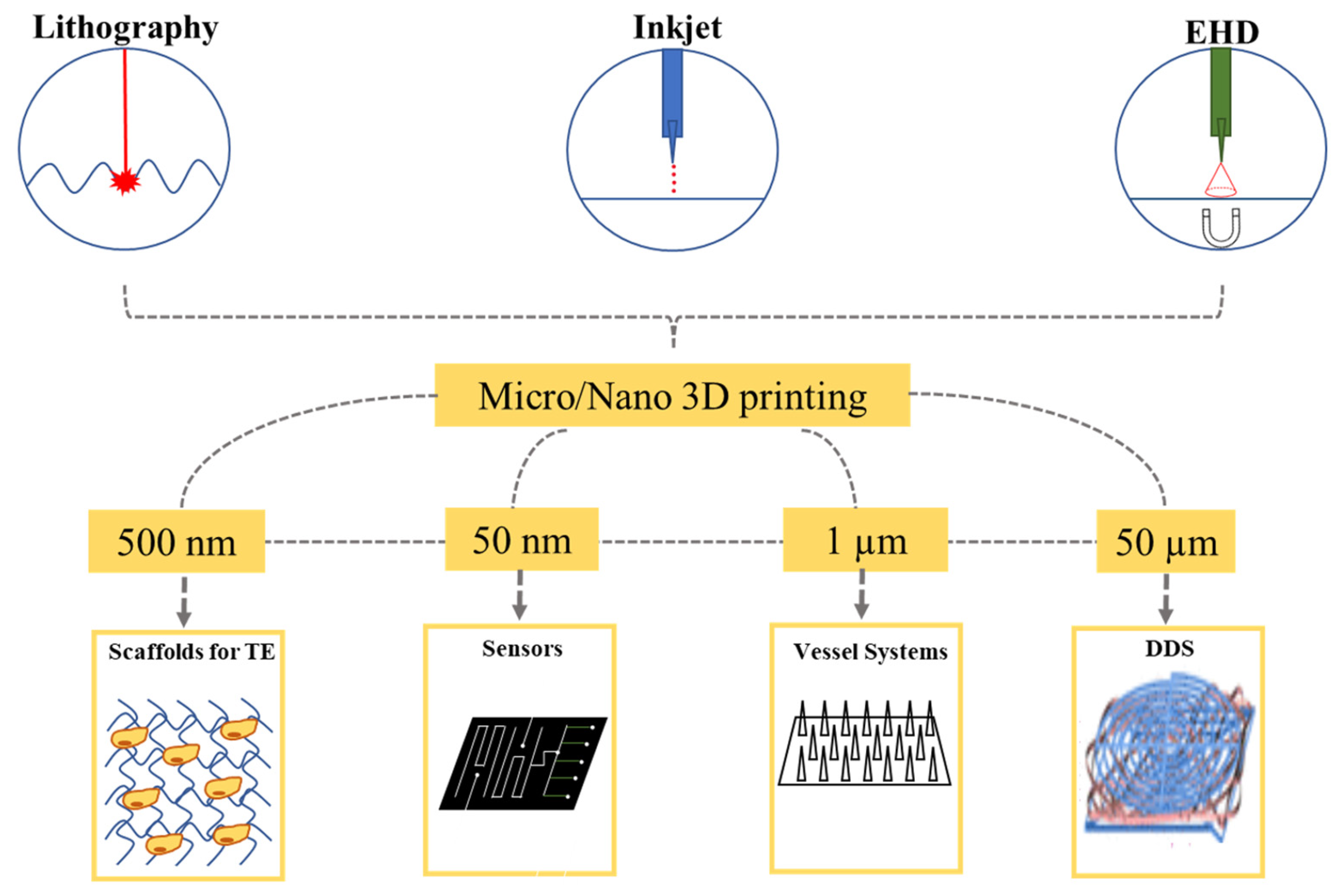
:1. Introduction
2. Micro-/Nano Printing Technologies
2.1. Stereolithography Printing
2.1.1. Two Photon Polymerization (TPP)
2.1.2. Dip-Pen Nanolithography (DPN)
2.2. Inkjet Printing
2.2.1. Piezoelectric Inkjet Printing
2.2.2. Thermal Inkjet Printing
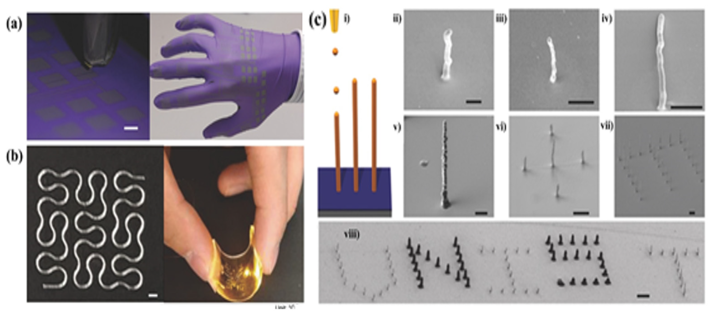
2.3. EHD Printing
2.3.1. Controlling Parameters
2.3.2. Process Parameters
2.3.3. Ink Physical Properties
2.3.4. Nozzle Structures
3. Printing Materials
3.1. Metals
3.2. Polymers
3.3. Ceramics/Composites


| Printable Material | Example | Application | Advantages | Disadvantages |
|---|---|---|---|---|
| Polymer | PCL PLA PVP Hydrogel |
|
|
|
| Metal | Au Ag Ti |
|
|
|
| Ceramic/ Composite | CaP Silica SiC |
|
|
|
4. Applications
4.1. Biomedical
4.1.1. Drug Delivery System (DDS)
4.1.2. Scaffolds for Tissue Regeneration
4.1.3. Vascular Structures
4.2. Electronic
4.2.1. Physical Sensor
4.2.2. Chemical Sensors
4.2.3. Hybrid Sensors

| 3DP Types | Sensing Materials | Types of Sensors | Application | Ref. |
|---|---|---|---|---|
| EHDP | Molten metal ink | Touch sensor | Flexible/stretchable devices | [65] |
| EHDP | Ag nanoink/ITO | Capacitive touch sensors | Flexible displays | [203] |
| EHDP | Molten polymer | Microcantilever sensor | Detecting multiple analytes | [207] |
| EHDP | PEDOT:PSS/NMP PEDOT:PSS/PVP/NMP PEDOT:PSS/PVP/Nafion/NMP | Pressure/strain sensor | Flexible robotic skin | [143] |
| EHDP | PEO/PANI/G | Piezoresistive sensor | Healthcare Environmental/bio-related monitoring | [151] |
| Inkjet P | TPU/CB | Piezoresistive sensor | Health monitoring Robotics tactile sensing Human machine interfaces | [66] |
| Inkjet P | Elastomer/pencil | Capacitive sensor | Touchpad Human-interface machine | [211] |
| Inkjet P | PET/Mylar/Ag NPs | Capacitive acoustic resonators | Navigation of drones | [205] |
| EHDP | PEDOT:PSS/poly(3-hexylthiophene-2,5-diyl) (P3HT) | Ion-gel transistor | Logic circuit Display backbone | [145] |
| EHDP | PEDOT:PSS | OTFT | Wearable sensor | [148] |
| EHDP | PEDOT:PSS/CNT | OTFT | Wearable sensor | [149] |
| EHDP | PVDF/BaTiO3 | Piezoelectric sensor | Gait analysis | [212] |
| Inkjet P | G/tungsten disulfide (WS2)/Si/SiO2 | Photosensor | Optical communications | [213] |
| Inkjet P | PVP/parylene-C/Ag nano ink | OTFT | Wearable sensor | [208] |
| EHDP | G ink | Photodetector | Optical communications | [214] |
| /(print) | G/WSe2/boron nitride (BN) | TFT | Optical communications | [209] |
| /(3DP) | Polylactic acid (PLA)/MWCNT | Liquid sensor | Substance detection | [220] |
| EHDP | MoS2 | Gas sensor | NO2/NH3 detection | [223] |
| Extrusion P | CNTs/PLA | Liquid sensor | Smart sensors in textile | [222] |
| Soft lithography assisted 3DP | Colorless resin | Microfluidics sensor | Analysis of nitrate in tap water | [221] |
| /(3DP) | G/PLA | Glucose biosensor | Glucose detection | [230] |
| /(3DP) | MXene/PEDOT: PSS | Electrochemical sensor | Nucleic acid detection | [228] |
| /(3DP) | MXene quantum dot-/liposome | Electrochemical sensor | Antibody detection | [229] |
| / | Reduced graphene oxide foam (rGOF) | Pressure/temperature sensor | Electronic skin | [232] |
| /(3DP) | PNIPAM/Laponite/CNT | Pressure/near-infrared light/temperature sensor | Human motion sensing Stimuli-responsive Electrical devices Wearable electronics | [234] |
| Inkjet P | Ag NPs | Resistive temperature | Environmental sensor | [235] |
| /(3DP) | CNT-ecoflex CNT-PDMS | capacitive/electrochemical sensor | Stretchable tactile/Electrochemical sensors | [236] |
| Inkjet P | Ag/PEDOT: PSS | humidity/temperature/compressive/strain sensor | Disposable biosensor Smart Packaging-labeling | [237] |
5. Conclusions
Author Contributions
Funding
Conflicts of Interest
References
- 3D Printing Market (2021–2026) | Industry Trends, Growth, Size—Mordor Intelligence. Available online: https://mordorintelligence.com/industry-reports/3d-printing-market (accessed on 5 February 2022).
- 3D Printing Market Size & Share Report, 2022–2030. Available online: https://www.grandviewresearch.com/industry-analysis/3d-printing-industry-analysis (accessed on 8 April 2022).
- Kucherov, F.A.; Romashov, L.V.; Ananikov, V.P. Development of 3D+G Printing for the Design of Customizable Flow Reactors. Chem. Eng. J. 2022, 430, 132670. [Google Scholar] [CrossRef]
- Murr, L.E. Metallurgy Principles Applied to Powder Bed Fusion 3D Printing/Additive Manufacturing of Personalized and Optimized Metal and Alloy Biomedical Implants: An Overview. J. Mater. Res. Technol. 2020, 9, 1087–1103. [Google Scholar] [CrossRef]
- Can Gold Melt at Room Temperature? Melting Temperature Depression!—Sustainable Nano. Available online: https://sustainable-nano.com/2018/02/14/melting-temperature-depression/ (accessed on 2 February 2022).
- Ru, C.; Luo, J.; Xie, S.; Sun, Y. A Review of Non-Contact Micro- and Nano-Printing Technologies. J. Micromech. Microeng. 2014, 24, 053001. [Google Scholar] [CrossRef] [Green Version]
- Huang, Y.; Wu, W.; Liu, H.; Chen, Y.; Li, B.; Gou, Z.; Li, X.; Gou, M. 3D Printing of Functional Nerve Guide Conduits. Burn. Trauma 2021, 9, tkab011. [Google Scholar] [CrossRef]
- Li, X.; Zhang, C.; Wu, S.; Chen, X.; Mai, J.; Chang, M.W. Precision Printing of Customized Cylindrical Capsules with Multifunctional Layers for Oral Drug Delivery. ACS Appl. Mater. Interfaces 2019, 11, 39179–39191. [Google Scholar] [CrossRef]
- Salonitis, K. Stereolithography. Compr. Mater. Process. 2014, 10, 19–67. [Google Scholar] [CrossRef]
- Yoon, H.S.; Jang, K.H.; Kim, E.; Lee, H.T.; Ahn, S.H. Hybrid 3D Printing by Bridging Micro/Nano Processes. J. Micromech. Microeng. 2017, 27, 065006. [Google Scholar] [CrossRef] [Green Version]
- Wei, Y.; Hu, Y.; Li, M.; Li, D. Fabrication of Sr-Functionalized Micro/Nano-Hierarchical Structure Ceramic Coatings on 3D Printing Titanium. Surf. Eng. 2020, 37, 373–380. [Google Scholar] [CrossRef]
- Singh, R.; Zhang, X.; Chen, Y.; Zheng, J.; Qin, H. In-Situ Real-Time Characterization of Micro-Filaments for Electrohydrodynamic Ink-Jet Printing Using Machine Vision. Procedia Manuf. 2018, 17, 45–52. [Google Scholar] [CrossRef]
- Wei, Y.; Hu, Y.; Li, M.; Li, D. Sr-Containing Micro/Nano-Hierarchical Textured TiO2 Nanotubes on 3D Printing Titanium. Inorg. Chem. Commun. 2020, 117, 107947. [Google Scholar] [CrossRef]
- Ahn, S.H.; Yoon, H.S.; Jang, K.H.; Kim, E.S.; Lee, H.T.; Lee, G.Y.; Kim, C.S.; Cha, S.W. Nanoscale 3D Printing Process Using Aerodynamically Focused Nanoparticle (AFN) Printing, Micro-Machining, and Focused Ion Beam (FIB). CIRP Ann. 2015, 64, 523–526. [Google Scholar] [CrossRef]
- Yang, L.; Wei, J.; Ma, Z.; Song, P.; Ma, J.; Zhao, Y.; Huang, Z.; Zhang, M.; Yang, F.; Wang, X. The Fabrication of Micro/Nano Structures by Laser Machining. Nanomaterials 2019, 9, 1789. [Google Scholar] [CrossRef] [PubMed] [Green Version]
- Ren, B.; Wan, Y.; Liu, C.; Wang, H.; Yu, M.; Zhang, X.; Huang, Y. Improved Osseointegration of 3D Printed Ti-6Al-4V Implant with a Hierarchical Micro/Nano Surface Topography: An in Vitro and in Vivo Study. Mater. Sci. Eng. C. Mater. Biol. Appl. 2021, 118, 111505. [Google Scholar] [CrossRef] [PubMed]
- Chen, C.; Jiang, J.; He, W.; Lei, W.; Hao, Q.; Zhang, X. 3D Printed High-Loading Lithium-Sulfur Battery Toward Wearable Energy Storage. Adv. Funct. Mater. 2020, 30, 1909469. [Google Scholar] [CrossRef]
- Wu, S.; Li, J.S.; Mai, J.; Chang, M.W. Three-Dimensional Electrohydrodynamic Printing and Spinning of Flexible Composite Structures for Oral Multidrug Forms. ACS Appl. Mater. Interf. 2018, 10, 24876–24885. [Google Scholar] [CrossRef]
- Fritzler, K.B.; Prinz, V.Y. 3D Printing Methods for Micro- and Nanostructures. Uspekhi Fiz. Nauk 2019, 189, 55–71. [Google Scholar] [CrossRef]
- Walker, J.L.; Santoro, M. Processing and Production of Bioresorbable Polymer Scaffolds for Tissue Engineering. In Bioresorbable Polymers for Biomedical Applications; Woodhead Publishing: Sawston, UK, 2017; pp. 181–203. [Google Scholar] [CrossRef]
- Singh, N. Additive Manufacturing for Functionalized Nanomaterials Breaks Limits. In Additive Manufacturing with Functionalized Nanomaterials; Elsevier: Amsterdam, The Netherlands, 2021; pp. 1–34. [Google Scholar] [CrossRef]
- Wang, L.; Luo, Y.; Ahmad, Z.; Li, J.S.; Chang, M.W. Fabrication of Stacked-Ring Netted Tubular Constructs via 3D Template Electrohydrodynamic Printing. J. Mater. Sci. 2018, 53, 11943–11950. [Google Scholar] [CrossRef]
- Dermanaki Farahani, R.; Dubé, M. Printing Polymer Nanocomposites and Composites in Three Dimensions. Adv. Eng. Mater. 2018, 20, 1700539. [Google Scholar] [CrossRef]
- Maruo, S. Stereolithography and Two-Photon Polymerization. In Handbook of Laser Micro- and Nano-Engineering; Springer: Berlin/Heidelberg, Germany, 2021; pp. 1–25. [Google Scholar] [CrossRef]
- Two-Photon Polymerization: A New Approach to Micromachining | Features | Oct 2006 | Photonics Spectra. Available online: https://www.photonics.com/Articles/Two-Photon_Polymerization_A_New_Approach_to/a26907 (accessed on 9 February 2022).
- Huang, Z.; Chi-Pong Tsui, G.; Deng, Y.; Tang, C.Y. Two-Photon Polymerization Nanolithography Technology for Fabrication of Stimulus-Responsive Micro/Nano-Structures for Biomedical Applications. Nanotechnol. Rev. 2020, 9, 1118–1136. [Google Scholar] [CrossRef]
- Coelho, S.; Baek, J.; Walsh, J.; Justin Gooding, J.; Gaus, K. Direct-Laser Writing for Subnanometer Focusing and Single-Molecule Imaging. Nat. Commun. 2022, 13, 647. [Google Scholar] [CrossRef]
- Hahn, V.; Messer, T.; Bojanowski, N.M.; Curticean, E.R.; Wacker, I.; Schröder, R.R.; Blasco, E.; Wegener, M.; Hahn, V.; Messer, T.; et al. Two-Step Absorption Instead of Two-Photon Absorption in 3D Nanoprinting. Nat. Photon 2021, 15, 932–938. [Google Scholar] [CrossRef]
- Spangenberg, A.; Hobeika, N.; Stehlin, F.; Malval, J.-P.; Wieder, F.; Prabhakaran, P.; Baldeck, P.; Soppera, O. Recent Advances in Two-Photon Stereolithography. In Updates in Advanced Lithography; Hosaka, S., Ed.; IntechOpen: London, UK, 2013; pp. 35–64. [Google Scholar]
- Yan, J.; Huang, Y.; Chrisey, D.B. Physics-Uspekhi instruments and methods of investigation 3D Printing Methods for Micro-and Nanostructures. Phys. Usp. 2019, 62, 54–69. [Google Scholar] [CrossRef]
- Thompson, J.R.; Worthington, K.S.; Green, B.J.; Mullin, N.K.; Jiao, C.; Kaalberg, E.E.; Wiley, L.A.; Han, I.C.; Russell, S.R.; Sohn, E.H.; et al. Two-Photon Polymerized Poly(Caprolactone) Retinal Cell Delivery Scaffolds and Their Systemic and Retinal Biocompatibility. Acta Biomater. 2019, 94, 204–218. [Google Scholar] [CrossRef] [PubMed]
- Stoneman, M.; Fox, M.; Zeng, C.; Raicu, V. Real-Time Monitoring of Two-Photon Photopolymerization for Use in Fabrication of Microfluidic Devices. Lab Chip 2009, 9, 819–827. [Google Scholar] [CrossRef] [PubMed]
- Liu, G.; Hirtz, M.; Fuchs, H.; Zheng, Z. Development of Dip-Pen Nanolithography (DPN) and Its Derivatives. Small 2019, 15, e1900564. [Google Scholar] [CrossRef]
- Khan, H.R.; Aamir, M.; Syed, A.S.; Akhtar, J. General Techniques for Preparation of Nanosensors. In Nanosensors for Smart Manufacturing; Elsevier: Amsterdam, The Netherlands, 2021; pp. 19–43. [Google Scholar] [CrossRef]
- Krivoshapkina, Y.; Kaestner, M.; Rangelow, I.W. Tip-Based Nanolithography Methods and Materials. Front. Nanosci. 2016, 11, 497–542. [Google Scholar] [CrossRef]
- Bhagoria, P.; Sebastian, E.M.; Jain, S.K.; Purohit, J.; Purohit, R. Nanolithography and Its Alternate Techniques. Mater. Today Proc. 2019, 26, 3048–3053. [Google Scholar] [CrossRef]
- Faia-Torres, A.B.; Goren, T.; Textor, M.; Pla-Roca, M. Patterned Biointerfaces. Compr. Biomater. II 2017, 4, 248–271. [Google Scholar] [CrossRef]
- Novembre, A.; Liu, S. Chemistry and Processing of Resists for Nanolithography. In Nanolithography; Woodhead Publishing: Sawston, UK, 2014; pp. 194–286. [Google Scholar] [CrossRef]
- Salaita, K.; Wang, Y.; Mirkin, C.A. Applications of Dip-Pen Nanolithography. Nat. Nanotechnol. 2007, 2, 145–155. [Google Scholar] [CrossRef]
- Li, H.; Wang, Z.; Huo, F.; Wang, S. Dip-Pen Nanolithography(DPN): From Micro/Nano-Patterns to Biosensing. Chem. Res. Chin. Univ. 2021, 37, 846–854. [Google Scholar] [CrossRef]
- Liu, G.; Rong, M.; Hu, H.; Chen, L.; Xie, Z.; Zheng, Z. 3D Dip-Pen Nanolithography. Adv. Mater. Technol. 2022, 2101493. [Google Scholar] [CrossRef]
- Zheng, F.; Wang, Z.; Huang, J.; Li, Z. Inkjet Printing-Based Fabrication of Microscale 3D Ice Structures. Microsyst. Nanoeng. 2020, 6, 89. [Google Scholar] [CrossRef]
- Farid, S.; Shirazi, S.; Gharehkhani, S.; Mehrali, M.; Yarmand, H.; Cornelis Metselaar, H.S.; Kadri, N.A.; Azuan, N.; Osman, A. A Review on Powder-Based Additive Manufacturing for Tissue Engineering: Selective Laser Sintering and Inkjet 3D Printing. Sci. Technol. Adv. Mater. 2015, 16, 033502. [Google Scholar] [CrossRef]
- Tappa, K.; Jammalamadaka, U. Functional Biomaterials Review Novel Biomaterials Used in Medical 3D Printing Techniques. J. Funct. Biomater. 2018, 9, 17. [Google Scholar] [CrossRef] [PubMed] [Green Version]
- McCoul, D.; Rosset, S.; Schlatter, S.; Shea, H. Inkjet 3D Printing of UV and Thermal Cure Silicone Elastomers for Dielectric Elastomer Actuators. Smart Mater. Struct. 2017, 26, 125022. [Google Scholar] [CrossRef] [Green Version]
- Duan, Y.; Ding, Y.; Xu, Z.; Huang, Y.; Yin, Z. Helix Electrohydrodynamic Printing of Highly Aligned Serpentine Micro/Nanofibers. Polymers 2017, 9, 434. [Google Scholar] [CrossRef] [Green Version]
- Zheng, F.; Huang, J.; Li, Z. Fabrication of 3D Micro Ice Structures Based on Inkjet Printing. In Proceedings of the 2019 IEEE 32nd International Conference on Micro Electro Mechanical Systems (MEMS), Seoul, Korea, 27–31 January 2019; pp. 368–371. [Google Scholar] [CrossRef]
- Jung, W.; Jung, Y.-H.; Pikhitsa, P.V.; Feng, J.; Yang, Y.; Kim, M.; Tsai, H.-Y.; Tanaka, T.; Shin, J.; Kim, K.-Y.; et al. Three-Dimensional Nanoprinting via Charged Aerosol Jets. Nature 2021, 592, 54–59. [Google Scholar] [CrossRef] [PubMed]
- Kullmann, C.; Schirmer, N.C.; Lee, M.T.; Ko, S.H.; Hotz, N.; Grigoropoulos, C.P.; Poulikakos, D. 3D Micro-Structures by Piezoelectric Inkjet Printing of Gold Nanofluids. J. Micromec. Microeng. 2012, 22, 055022. [Google Scholar] [CrossRef]
- Guo, Y.; Patanwala, H.S.; Bognet, B.; Ma, A.W.K. Inkjet and Inkjet-Based 3D Printing: Connecting Fluid Properties and Printing Performance. Rapid Prototyp. J. 2017, 23, 562–576. [Google Scholar] [CrossRef]
- Kuznetsova, I.; Smirnov, A.; Anisimkin, V.; Gubin, S.; Signore, M.A.; Francioso, L.; Kondoh, J.; Kolesov, V. Inkjet Printing of Plate Acoustic Wave Devices. Sensors 2020, 20, 3349. [Google Scholar] [CrossRef]
- Gomes, T.C.; Constantino, C.J.L.; Lopes, E.M.; Job, A.E.; Alves, N. Thermal Inkjet Printing of Polyaniline on Paper. Thin Solid Films 2012, 520, 7200–7204. [Google Scholar] [CrossRef]
- Li, C.; Shi, H.; Ran, R.; Su, C.; Shao, Z. Thermal Inkjet Printing of Thin-Film Electrolytes and Buffering Layers for Solid Oxide Fuel Cells with Improved Performance. Int. J. Hydrogen Energy 2013, 38, 9310–9319. [Google Scholar] [CrossRef]
- Cui, X.; Boland, T.; D’lima, D.D.; Lotz, M.K. Thermal Inkjet Printing in Tissue Engineering and Regenerative Medicine. Recent Patents Drug Deliv. Formul. 2012, 6, 149–155. [Google Scholar] [CrossRef] [PubMed]
- Magazine, R.; van Bochove, B.; Borandeh, S.; Seppälä, J. 3D Inkjet-Printing of Photo-Crosslinkable Resins for Microlens Fabrication. Addit. Manuf. 2022, 50, 102534. [Google Scholar] [CrossRef]
- Setti, L.; Fraleoni-Morgera, A.; Mencarelli, I.; Filippini, A.; Ballarin, B.; Di Biase, M. An HRP-Based Amperometric Biosensor Fabricated by Thermal Inkjet Printing. Sens. Actuators B Chem. 2007, 126, 252–257. [Google Scholar] [CrossRef]
- Huang, Z.; Tang, Y.; Guo, H.; Feng, X.; Zhang, T.; Li, P.; Qian, B.; Xie, Y. 3D Printing of Ceramics and Graphene Circuits-on-Ceramics by Thermal Bubble Inkjet Technology and High Temperature Sintering. Ceram. Int. 2020, 46, 10096–10104. [Google Scholar] [CrossRef]
- Cui, X.; Boland, T. Human Microvasculature Fabrication Using Thermal Inkjet Printing Technology. Biomaterials 2009, 30, 6221–6227. [Google Scholar] [CrossRef] [PubMed] [Green Version]
- Wu, S.; Ahmad, Z.; Li, J.S.; Chang, M.W. Fabrication of Flexible Composite Drug Films via Foldable Linkages Using Electrohydrodynamic Printing. Mater. Sci. Eng. C 2020, 108, 110393. [Google Scholar] [CrossRef]
- Cheng, E.; Zhang, T.; Cheng, Y.; Li, J.; Zhang, Z. High Scaling Ratio Line Width Reduction and Fabrication Method with Electrohydrodynamic Jet Printing. Micro Nano Lett. 2021, 16, 23–29. [Google Scholar] [CrossRef]
- Liu, Y.; Huang, Y. Theoretical and Experimental Studies of Electrostatic Focusing for Electrohydrodynamic Jet Printing. J. Micromech. Microeng. 2019, 29, 65002. [Google Scholar] [CrossRef]
- He, J.; Xu, F.; Cao, Y.; Liu, Y.; Li, D. Towards Microscale Electrohydrodynamic Three-Dimensional Printing. J. Phys. D. Appl. Phys. 2016, 49, 55504. [Google Scholar] [CrossRef]
- Wu, Y. Electrohydrodynamic Jet 3D Printing in Biomedical Applications. Acta Biomater. 2021, 128, 21–41. [Google Scholar] [CrossRef] [PubMed]
- Kim, B.H.; Onses, M.S.; Bin Lim, J.; Nam, S.; Oh, N.; Kim, H.; Yu, K.J.; Lee, J.W.; Kim, J.-H.; Kang, S.-K.; et al. High-Resolution Patterns of Quantum Dots Formed by Electrohydrodynamic Jet Printing for Light-Emitting Diodes. Nano Lett. 2015, 15, 969–973. [Google Scholar] [CrossRef] [PubMed] [Green Version]
- Han, Y.; Dong, J. Electrohydrodynamic (EHD) Printing of Molten Metal Ink for Flexible and Stretchable Conductor with Self-Healing Capability. Adv. Mater. Technol. 2018, 3, 1700268. [Google Scholar] [CrossRef]
- Wang, Z.; Guan, X.; Huang, H.; Wang, H.; Lin, W.; Peng, Z. Full 3D Printing of Stretchable Piezoresistive Sensor with Hierarchical Porosity and Multimodulus Architecture. Adv. Funct. Mater. 2019, 29, 1807569. [Google Scholar] [CrossRef]
- Lee, S.; Choi, J. Microelectromechanical Systems Print Heads for Industrial Printing. In Smart Sensors and MEMS: Intelligent Sensing Devices and Microsystems for Industrial Applications, 2nd ed.; Woodhead Publishing: Sawston, UK, 2018; pp. 429–460. ISBN 9780081020562. [Google Scholar]
- Fang, F.; Aabith, S.; Homer-Vanniasinkam, S.; Tiwari, M.K. High-Resolution 3D Printing for Healthcare Underpinned by Small-Scale Fluidics. In 3D Printing in Medicine; Woodhead Publishing: Sawston, UK, 2017; pp. 167–206. [Google Scholar] [CrossRef]
- Onses, M.S.; Sutanto, E.; Ferreira, P.M.; Alleyne, A.G.; Rogers, J.A. Mechanisms, Capabilities, and Applications of High-Resolution Electrohydrodynamic Jet Printing. Small 2015, 11, 4237–4266. [Google Scholar] [CrossRef]
- Zhang, C.; Chang, M.W.; Ahmad, Z.; Hu, W.; Zhao, D.; Li, J.S. Stable Single Device Multi-Pore Electrospraying of Polymeric Microparticles via Controlled Electrostatic Interactions. RSC Adv. 2015, 5, 87919–87923. [Google Scholar] [CrossRef]
- Han, Y.; Dong, J. Electrohydrodynamic Printing for Advanced Micro/Nanomanufacturing: Current Progresses, Opportunities, and Challenges. J. Micro Nano-Manuf. 2018, 6, 040802. [Google Scholar] [CrossRef]
- Abbas, Z.; Wang, D.; Du, Z.; Zhao, K.; Du, Z.; Lu, L.; Cui, Y.; Liang, J. Numerical Simulation of Stable Electrohydrodynamic Cone-Jet Formation and Printing on Flexible Substrate. Microelectron. Eng. 2021, 237, 111496. [Google Scholar] [CrossRef]
- Choi, H.K.; Park, J.-U.; Park, O.O.; Ferreira, P.M.; Georgiadis, J.G.; Rogers, J.A. Scaling Laws for Jet Pulsations Associated with High-Resolution Electrohydrodynamic Printing. Appl. Phys. Lett. 2008, 92, 123109. [Google Scholar] [CrossRef] [Green Version]
- Jaworek, A.; Sobczyk, A.T. Electrospraying Route to Nanotechnology: An Overview. J. Electrostat. 2008, 66, 197–219. [Google Scholar] [CrossRef]
- Rahmat, A.; Koc, B.; Yildiz, M. A Systematic Study on Numerical Simulation of Electrified Jet Printing. Addit. Manuf. 2017, 18, 15–21. [Google Scholar] [CrossRef]
- Hartman, R.P.A.; Brunner, D.J.; Camelot, D.M.A.; Marijnissen, J.C.M.; Scarlett, B. Electrohydrodynamic Atomization in The Cone–Jet Mode Physical Modeling of The Liquid Cone And Jet. J. Aerosol Sci. 1999, 30, 823–849. [Google Scholar] [CrossRef]
- Collins, R.T.; Harris, M.T.; Basaran, O.A. Breakup of Electrified Jets. J. Fluid Mech. 2007, 588, 75–129. [Google Scholar] [CrossRef] [Green Version]
- Jaworek, A.; Krupa, A. Jet and Drops Formation in Electrohydrodynamic Spraying of Liquids. A Systematic Approach. Exp. Fluids 1999, 27, 43–52. [Google Scholar] [CrossRef]
- Mkhize, N.; Bhaskaran, H. Electrohydrodynamic Jet Printing: Introductory Concepts and Considerations. Small Sci. 2022, 2, 2100073. [Google Scholar] [CrossRef]
- Cai, S.; Sun, Y.; Wang, Z.; Yang, W.; Li, X.; Yu, H. Mechanisms, Influencing Factors, and Applications of Electrohydrodynamic Jet Printing. Nanotechnol. Rev. 2021, 10, 1046–1078. [Google Scholar] [CrossRef]
- Kwon, H.J.; Hong, J.; Nam, S.Y.; Choi, H.H.; Li, X.; Jeong, Y.J.; Kim, S.H. Overview of Recent Progress in Electrohydrodynamic Jet Printing in Practical Printed Electronics: Focus on the Variety of Printable Materials for Each Component. Mater. Adv. 2021, 2, 5593–5615. [Google Scholar] [CrossRef]
- Park, J.-U.; Hardy, M.; Kang, S.J.; Barton, K.; Adair, K.; Mukhopadhyay, D.K.; Lee, C.Y.; Strano, M.S.; Alleyne, A.G.; Georgiadis, J.G.; et al. High-Resolution Electrohydrodynamic Jet Printing. Nat. Mater. 2007, 6, 782–789. [Google Scholar] [CrossRef]
- Kim, W.; Kim, S.S. Synthesis of Biodegradable Triple-Layered Capsules Using a Triaxial Electrospray Method. Polymer 2011, 52, 3325–3336. [Google Scholar] [CrossRef]
- Mehta, P.; Zaman, A.; Smith, A.; Rasekh, M.; Haj-Ahmad, R.; Arshad, M.S.; van der Merwe, S.; Chang, M.-W.; Ahmad, Z. Broad Scale and Structure Fabrication of Healthcare Materials for Drug and Emerging Therapies via Electrohydrodynamic Techniques. Adv. Ther. 2019, 2, 1800024. [Google Scholar] [CrossRef] [Green Version]
- Pan, Y.; Zeng, L. Simulation and Validation of Droplet Generation Process for Revealing Three Design Constraints in Electrohydrodynamic Jet Printing. Micromachines 2019, 10, 94. [Google Scholar] [CrossRef] [PubMed] [Green Version]
- Enayati, M.; Chang, M.W.; Bragman, F.; Edirisinghe, M.; Stride, E. Electrohydrodynamic Preparation of Particles, Capsules and Bubbles for Biomedical Engineering Applications. Colloids Surf. A Physicochem. Eng. Asp. 2011, 382, 154–164. [Google Scholar] [CrossRef]
- Mohammadi, K.; Movahhedy, M.R.; Khodaygan, S. A Multiphysics Model for Analysis of Droplet Formation in Electrohydrodynamic 3D Printing Process. J. Aerosol Sci. 2019, 135, 72–85. [Google Scholar] [CrossRef]
- Yao, Z.C.; Wang, J.C.; Wang, B.; Ahmad, Z.; Li, J.S.; Chang, M.W. A Novel Approach for Tailored Medicines: Direct Writing of Janus Fibers. J. Drug Deliv. Sci. Technol. 2019, 50, 372–379. [Google Scholar] [CrossRef]
- Wang, B.; Chen, X.; Ahmad, Z.; Huang, J.; Chang, M.W. Engineering On-Demand Magnetic Core–Shell Composite Wound Dressing Matrices via Electrohydrodynamic Micro-Scale Printing. Adv. Eng. Mater. 2019, 21, 1900699. [Google Scholar] [CrossRef]
- Su, S.; Liang, J.; Wang, Z.; Xin, W.; Li, X.; Wang, D. Microtip Focused Electrohydrodynamic Jet Printing with Nanoscale Resolution. Nanoscale 2020, 12, 24450–24462. [Google Scholar] [CrossRef]
- Lee, M.W.; Kang, D.K.; Kim, N.Y.; Kim, H.Y.; James, S.C.; Yoon, S.S. A Study of Ejection Modes for Pulsed-DC Electrohydrodynamic Inkjet Printing. J. Aerosol Sci. 2012, 46, 1–6. [Google Scholar] [CrossRef]
- Zhang, B.; Lee, J.; Kim, M.; Lee, N.; Lee, H.; Byun, D. Direct Patterning and Spontaneous Self-Assembly of Graphene Oxide via Electrohydrodynamic Jet Printing for Energy Storage and Sensing. Micromachines 2019, 11, 13. [Google Scholar] [CrossRef] [Green Version]
- Moghadam, H.; Samimi, M.; Samimi, A.; Khorram, M. Electrospray Modeling of Highly Viscous and Non-Newtonian Liquids. J. Appl. Polym. Sci. 2010, 118, 1288–1296. [Google Scholar] [CrossRef]
- Lee, A.; Jin, H.; Dang, H.-W.; Choi, K.-H.; Ahn, K.H. Optimization of Experimental Parameters to Determine the Jetting Regimes in Electrohydrodynamic Printing. Langmuir 2013, 29, 13630–13639. [Google Scholar] [CrossRef] [PubMed]
- Liashenko, I.; Rosell-Llompart, J.; Cabot, A. Ultrafast 3D Printing with Submicrometer Features Using Electrostatic Jet Deflection. Nat. Commun. 2020, 11, 753. [Google Scholar] [CrossRef] [PubMed]
- Jiang, C.; Wang, K.; Jiang, X.; Zhang, C.; Wang, B. Quantitative Investigation of the Process Parameters of Electrohydrodynamic Direct-Writing and Their Effects on Fiber Surface Roughness and Cell Adhesion. Polymers 2020, 12, 2475. [Google Scholar] [CrossRef] [PubMed]
- Kim, S.-Y.; Kim, Y.; Park, J.; Hwang, J. Design and Evaluation of Single Nozzle with a Non-Conductive Tip for Reducing Applied Voltage and Pattern Width in Electrohydrodynamic Jet Printing (EHDP). J. Micromech. Microeng. 2010, 20, 55009. [Google Scholar] [CrossRef]
- Cui, Z.; Han, Y.; Huang, Q.; Dong, J.; Zhu, Y. Electrohydrodynamic Printing of Silver Nanowires for Flexible and Stretchable Electronics. Nanoscale 2018, 10, 6806–6811. [Google Scholar] [CrossRef]
- He, J.; Xu, F.; Cao, Y.; Liu, Y.; Li, D.; Jin, Z. Electrohydrodynamic Direct-Writing Lithography: An Alternative Maskless Technique for Microstructure Fabrication. Appl. Phys. Lett. 2014, 105, 253109. [Google Scholar] [CrossRef]
- Bin Bu, N.; Huang, Y.A.; Yin, Z.P. The Effect of Substrate on Continuous Electrohydrodynamic Printing. Adv. Mater. Res. 2013, 684, 352–356. [Google Scholar] [CrossRef]
- Wang, B.; Zhou, W.; Chang, M.W.; Ahmad, Z.; Li, J.S. Impact of Substrate Geometry on Electrospun Fiber Deposition and Alignment. J. Appl. Polym. Sci. 2017, 134. [Google Scholar] [CrossRef]
- Huang, Q.; Zhu, Y. Printing Conductive Nanomaterials for Flexible and Stretchable Electronics: A Review of Materials, Processes, and Applications. Adv. Mater. Technol. 2019, 4, 1800546. [Google Scholar] [CrossRef]
- Wang, J.C.; Chang, M.W.; Ahmad, Z.; Li, J.S. Fabrication of Patterned Polymer-Antibiotic Composite Fibers via Electrohydrodynamic (EHD) Printing. J. Drug Deliv. Sci. Technol. 2016, 35, 114–123. [Google Scholar] [CrossRef]
- Yuk, H.; Lu, B.; Lin, S.; Qu, K.; Xu, J.; Luo, J.; Zhao, X. 3D Printing of Conducting Polymers. Nat. Commun. 2020, 11, 1604. [Google Scholar] [CrossRef] [PubMed] [Green Version]
- Yu, M.; Ahn, K.H.; Lee, S.J. Design Optimization of Ink in Electrohydrodynamic Jet Printing: Effect of Viscoelasticity on the Formation of Taylor Cone Jet. Mater. Des. 2016, 89, 109–115. [Google Scholar] [CrossRef]
- Bae, J.; Lee, J.; Hyun Kim, S. Effects of Polymer Properties on Jetting Performance of Electrohydrodynamic Printing. J. Appl. Polym. Sci. 2017, 134, 45044. [Google Scholar] [CrossRef]
- Zhang, C.; Chang, M.-W.; Li, Y.; Qi, Y.; Wu, J.; Ahmad, Z.; Li, J.-S. Janus Particle Synthesis via Aligned Non-Concentric Angular Nozzles and Electrohydrodynamic Co-Flow for Tunable Drug Release. RSC Adv. 2016, 6, 77174–77178. [Google Scholar] [CrossRef]
- Zhang, C.; Gao, C.; Chang, M.W.; Ahmad, Z.; Li, J.S. Continuous Micron-Scaled Rope Engineering Using a Rotating Multi-Nozzle Electrospinning Emitter. Appl. Phys. Lett. 2016, 109, 151903. [Google Scholar] [CrossRef]
- Pan, Y.; Chen, X.; Zeng, L.; Huang, Y.; Yin, Z. Fabrication and Evaluation of a Protruding Si-Based Printhead for Electrohydrodynamic Jet Printing. J. Micromech. Microeng. 2017, 27, 125004. [Google Scholar] [CrossRef]
- Zhu, L.F.; Chen, X.; Ahmad, Z.; Li, J.S.; Chang, M.W. Engineering of Ganoderma Lucidum Polysaccharide Loaded Polyvinyl Alcohol Nanofibers for Biopharmaceutical Delivery. J. Drug Deliv. Sci. Technol. 2019, 50, 208–216. [Google Scholar] [CrossRef]
- Wang, J.C.; Zheng, H.; Chang, M.W.; Ahmad, Z.; Li, J.S. Preparation of Active 3D Film Patches via Aligned Fiber Electrohydrodynamic (EHD) Printing. Sci. Rep. 2017, 7, srep43924. [Google Scholar] [CrossRef] [Green Version]
- Yu, J.H.; Kim, S.Y.; Hwang, J. Effect of Viscosity of Silver Nanoparticle Suspension on Conductive Line Patterned by Electrohydrodynamic Jet Printing. Appl. Phys. A 2007, 89, 157–159. [Google Scholar] [CrossRef]
- Park, J.U.; Lee, J.H.; Paik, U.; Lu, Y.; Rogers, J.A. Nanoscale Patterns of Oligonucleotides Formed by Electrohydrodynamic Jet Printing with Applications in Biosensing and Nanomaterials Assembly. Nano Lett. 2008, 8, 4210–4216. [Google Scholar] [CrossRef]
- Kim, Y.; Jang, S.; Oh, J.H. High-Resolution Electrohydrodynamic Printing of Silver Nanoparticle Ink via Commercial Hypodermic Needles. Appl. Phys. Lett. 2015, 106, 14103. [Google Scholar] [CrossRef]
- Zou, W.; Yu, H.; Zhou, P.; Liu, L. Tip-Assisted Electrohydrodynamic Jet Printing for High-Resolution Microdroplet Deposition. Mater. Des. 2019, 166, 107609. [Google Scholar] [CrossRef]
- Han, Y.; Dong, J. Design of Integrated Ring Extractor for High Resolution Electrohydrodynamic (EHD) 3D Printing. Procedia Manuf. 2016, 5, 1031–1042. [Google Scholar] [CrossRef] [Green Version]
- Zhang, X.; Kobayashi, I.; Uemura, K.; Nakajima, M. Direct Observation and Characterization of the Generation of Organic Solvent Droplets with and without Triglyceride Oil by Electrospraying. Colloids Surf. A Physicochem. Eng. Asp. 2013, 436, 937–943. [Google Scholar] [CrossRef] [Green Version]
- Lee, D.-Y.; Shin, Y.-S.; Park, S.-E.; Yu, T.-U.; Hwang, J. Electrohydrodynamic Printing of Silver Nanoparticles by Using a Focused Nanocolloid Jet. Appl. Phys. Lett. 2007, 90, 81905. [Google Scholar] [CrossRef] [Green Version]
- Lee, J.S.; Kim, S.Y.; Kim, Y.J.; Park, J.; Kim, Y.; Hwang, J.; Kim, Y.J. Design and Evaluation of a Silicon Based Multi-Nozzle for Addressable Jetting Using a Controlled Flow Rate in Electrohydrodynamic Jet Printing. Appl. Phys. Lett. 2008, 93, 243114. [Google Scholar] [CrossRef]
- Khan, A.; Rahman, K.; Kim, D.S.; Choi, K.H. Direct Printing of Copper Conductive Micro-Tracks by Multi-Nozzle Electrohydrodynamic Inkjet Printing Process. J. Mater. Process. Technol. 2012, 212, 700–706. [Google Scholar] [CrossRef]
- Wang, B.; Ahmad, Z.; Huang, J.; Li, J.; Chang, M.-W. Development of Random and Ordered Composite Fiber Hybrid Technologies for Controlled Release Functions. Chem. Eng. J. 2018, 343, 379–389. [Google Scholar] [CrossRef]
- Wang, B.; Wu, S.; Ahmad, Z.; Li, J.-S.; Chang, M.W. Co-Printing of Vertical Axis Aligned Micron-Scaled Filaments via Simultaneous Dual Needle Electrohydrodynamic Printing. Eur. Polym. J. 2018, 104, 81–89. [Google Scholar] [CrossRef]
- Yao, Z.C.; Wang, J.C.; Ahmad, Z.; Li, J.S.; Chang, M.W. Fabrication of Patterned Three-Dimensional Micron Scaled Core-Sheath Architectures for Drug Patches. Mater. Sci. Eng. C 2019, 97, 776–783. [Google Scholar] [CrossRef]
- Wang, B.; Chen, X.; Ahmad, Z.; Huang, J.; Chang, M.W. 3D Electrohydrodynamic Printing of Highly Aligned Dual-Core Graphene Composite Matrices. Carbon N. Y. 2019, 153, 285–297. [Google Scholar] [CrossRef]
- Li, H.; Zhu, X.; Li, Z.; Yang, J.; Lan, H. Preparation of Nano Silver Paste and Applications in Transparent Electrodes via Electric-Field Driven Micro-Scale 3D Printing. Nanomaterials 2020, 10, 107. [Google Scholar] [CrossRef] [PubMed] [Green Version]
- Ni, J.; Ling, H.; Zhang, S.; Wang, Z.; Peng, Z.; Benyshek, C.; Zan, R.; Miri, A.K.; Li, Z.; Zhang, X.; et al. Three-Dimensional Printing of Metals for Biomedical Applications. Mater. Today Bio. 2019, 3, 10024. [Google Scholar] [CrossRef] [PubMed]
- Nocheseda, C.J.C.; Liza, F.P.; Collera, A.K.M.; Caldona, E.B.; Advincula, R.C. 3D Printing of Metals Using Biodegradable Cellulose Hydrogel Inks. Addit. Manuf. 2021, 48, 102380. [Google Scholar] [CrossRef]
- Khorsandi, D.; Fahimipour, A.; Abasian, P.; Saber, S.S.; Seyedi, M.; Ghanavati, S.; Ahmad, A.; De Stephanis, A.A.; Taghavinezhaddilami, F.; Leonova, A.; et al. 3D and 4D Printing in Dentistry and Maxillofacial Surgery: Printing Techniques, Materials, and Applications. Acta Biomater. 2021, 122, 26–49. [Google Scholar] [CrossRef] [PubMed]
- Dickey, M.D. Stretchable and Soft Electronics Using Liquid Metals. Adv. Mater. 2017, 29, 1606425. [Google Scholar] [CrossRef]
- Wang, X.; Liu, J. Recent Advancements in Liquid Metal Flexible Printed Electronics: Properties, Technologies, and Applications. Micromachines 2016, 7, 206. [Google Scholar] [CrossRef]
- Boley, J.W.; White, E.L.; Kramer, R.K. Mechanically Sintered Gallium–Indium Nanoparticles. Adv. Mater. 2015, 27, 2355–2360. [Google Scholar] [CrossRef]
- Xu, F.; Zhu, Y. Highly Conductive and Stretchable Silver Nanowire Conductors. Adv. Mater. 2012, 24, 5117–5122. [Google Scholar] [CrossRef]
- Chu, T.-Y.; Zhang, Z.; Tao, Y. Printing Silver Conductive Inks with High Resolution and High Aspect Ratio. Adv. Mater. Technol. 2018, 3, 1700321. [Google Scholar] [CrossRef]
- Park, M.; Im, J.; Shin, M.; Min, Y.; Park, J.; Cho, H.; Park, S.; Shim, M.-B.; Jeon, S.; Chung, D.-Y.; et al. Highly Stretchable Electric Circuits from a Composite Material of Silver Nanoparticles and Elastomeric Fibres. Nat. Nanotechnol. 2012, 7, 803–809. [Google Scholar] [CrossRef] [PubMed]
- He, F.; You, X.; Wang, W.; Bai, T.; Xue, G.; Ye, M. Recent Progress in Flexible Microstructural Pressure Sensors toward Human–Machine Interaction and Healthcare Applications. Small Methods 2021, 5, 2001041. [Google Scholar] [CrossRef] [PubMed]
- Rim, Y.S.; Bae, S.H.; Chen, H.; De Marco, N.; Yang, Y. Recent Progress in Materials and Devices toward Printable and Flexible Sensors. Adv. Mater. 2016, 28, 4415–4440. [Google Scholar] [CrossRef] [PubMed]
- Hou, Z.; Lu, H.; Li, Y.; Yang, L.; Gao, Y. Direct Ink Writing of Materials for Electronics-Related Applications: A Mini Review. Front. Mater. 2021, 8, 91. [Google Scholar] [CrossRef]
- Pugliese, R.; Beltrami, B.; Regondi, S.; Lunetta, C. Polymeric Biomaterials for 3D Printing in Medicine: An Overview. Ann. 3D Print. Med. 2021, 2, 100011. [Google Scholar] [CrossRef]
- Liu, M.-M.; Zhong, Y.; Chen, Y.; Wu, L.-N.; Chen, W.; Lin, X.-H.; Lei, Y.; Liu, A.-L. Electrochemical Monitoring the Effect of Drug Intervention on PC12 Cell Damage Model Cultured on Paper-PLA 3D Printed Device. Anal. Chim. Acta 2022, 1194, 339409. [Google Scholar] [CrossRef]
- Emon, O.F.; Alkadi, F.; Kiki, M.; Choi, J.-W. Conformal 3D Printing of a Polymeric Tactile Sensor. Addit. Manuf. Lett. 2022, 2, 100027. [Google Scholar] [CrossRef]
- Wang, T.; Zhang, Y.; Liu, Q.; Cheng, W.; Wang, X.; Pan, L.; Xu, B.; Xu, H. A Self-Healable, Highly Stretchable, and Solution Processable Conductive Polymer Composite for Ultrasensitive Strain and Pressure Sensing. Adv. Funct. Mater. 2018, 28, 1705551. [Google Scholar] [CrossRef]
- Chang, J.; He, J.; Lei, Q.; Li, D. Electrohydrodynamic Printing of Microscale PEDOT:PSS-PEO Features with Tunable Conductive/Thermal Properties. ACS Appl. Mater. Interf. 2018, 10, 19116–19122. [Google Scholar] [CrossRef]
- Nothnagle, C.; Baptist, J.R.; Sanford, J.; Lee, W.H.; Popa, D.O.; Wijesundara, M.B.J. EHD Printing of PEDOT: PSS Inks for Fabricating Pressure and Strain Sensor Arrays on Flexible Substrates. In Proceedings of the Volume 9494, Next-Generation Robotics II and Machine Intelligence and Bio-inspired Computation: Theory and Applications IX, Baltimore, MD, USA, 2 June 2015; Volume 9494. [Google Scholar]
- Mirza, F.; Sahasrabuddhe, R.R.; Baptist, J.R.; Wijesundara, M.B.J.; Lee, W.H.; Popa, D.O. Piezoresistive Pressure Sensor Array for Robotic Skin. In Proceedings of the Sensors for Next-Generation Robotics III, Baltimore, MD, USA, 13 May 2016; Volume 9859. [Google Scholar]
- Jung, E.M.; Lee, S.W.; Kim, S.H. Printed Ion-Gel Transistor Using Electrohydrodynamic (EHD) Jet Printing Process. Org. Electron. 2018, 52, 123–129. [Google Scholar] [CrossRef]
- Lim, S.; Park, S.H.; An, T.K.; Lee, H.S.; Kim, S.H. Electrohydrodynamic Printing of Poly(3,4-Ethylenedioxythiophene):Poly(4-Styrenesulfonate) Electrodes with Ratio-Optimized Surfactant. RSC Adv. 2016, 6, 2004–2010. [Google Scholar] [CrossRef]
- Lyu, B.; Im, S.; Jing, H.; Lee, S.; Kim, S.H.; Kim, J.H.; Cho, J.H. Work Function Engineering of Electrohydrodynamic-Jet-Printed PEDOT:PSS Electrodes for High-Performance Printed Electronics. ACS Appl. Mater. Interf. 2020, 12, 17799–17805. [Google Scholar] [CrossRef] [PubMed]
- Park, S.H.; Kim, J.; Park, C.E.; Lee, J.; Lee, H.S.; Lim, S.; Kim, S.H. Optimization of Electrohydrodynamic-Printed Organic Electrodes for Bottom-Contact Organic Thin Film Transistors. Org. Electron. 2016, 38, 48–54. [Google Scholar] [CrossRef]
- Park, S.H.; Kim, J.; Lee, S.; Lee, D.Y.; Lim, S.; Lee, J.; Kim, S.H. Organic Thin-Film Transistors with Sub-10-Micrometer Channel Length with Printed Polymer/Carbon Nanotube Electrodes. Org. Electron. 2018, 52, 165–171. [Google Scholar] [CrossRef]
- Tang, X.; Kwon, H.J.; Ye, H.; Kim, J.Y.; Lee, J.; Jeong, Y.J.; Kim, S.H. Enhanced Solvent Resistance and Electrical Performance of Electrohydrodynamic Jet Printed PEDOT:PSS Composite Patterns: Effects of Hardeners on the Performance of Organic Thin-Film Transistors. Phys. Chem. Chem. Phys. 2019, 21, 25690–25699. [Google Scholar] [CrossRef]
- Song, Y.; Dong, H.; Liu, W.; Fu, X.; Fu, Z.; Li, P.; Chen, L.; Ahmad, Z.; Liu, J.; Chen, X.; et al. Electrostatic Jet Engineering of Flexible Composite Pressure Sensors for Physical Applications. ACS Appl. Polym. Mater. 2022, 4, 868–878. [Google Scholar] [CrossRef]
- Liu, C.; Huang, N.; Xu, F.; Tong, J.; Chen, Z.; Gui, X.; Fu, Y.; Lao, C. 3D Printing Technologies for Flexible Tactile Sensors toward Wearable Electronics and Electronic Skin. Polymers 2018, 10, 629. [Google Scholar] [CrossRef] [Green Version]
- Li, J.; Fang, L.; Sun, B.; Li, X.; Kang, S.H. Review—Recent Progress in Flexible and Stretchable Piezoresistive Sensors and Their Applications. J. Electrochem. Soc. 2020, 167, 37561. [Google Scholar] [CrossRef]
- Koroglu, L.; Ayas, E.; Ay, N. 3D Printing of Polyvinylidene Fluoride Based Piezoelectric Nanocomposites: An Overview. Macromol. Mater. Eng. 2021, 306, 2100277. [Google Scholar] [CrossRef]
- Pagac, M.; Hajnys, J.; Ma, Q.-P.; Jancar, L.; Jansa, J.; Stefek, P.; Mesicek, J. A Review of Vat Photopolymerization Technology: Materials, Applications, Challenges, and Future Trends of 3D Printing. Polymers 2021, 13, 598. [Google Scholar] [CrossRef]
- Zhou, L.; Gao, Q.; Fu, J.; Chen, Q.; Zhu, J.; Sun, Y.; He, Y. Multimaterial 3D Printing of Highly Stretchable Silicone Elastomers. ACS Appl. Mater. Interf. 2019, 11, 23573–23583. [Google Scholar] [CrossRef] [PubMed]
- Valentine, A.D.; Busbee, T.A.; Boley, J.W.; Raney, J.R.; Chortos, A.; Kotikian, A.; Berrigan, J.D.; Durstock, M.F.; Lewis, J.A. Hybrid 3D Printing of Soft Electronics. Adv. Mater. 2017, 29, 1703817. [Google Scholar] [CrossRef] [PubMed]
- Tawk, C.; in het Panhuis, M.; Spinks, G.M.; Alici, G. Bioinspired 3D Printable Soft Vacuum Actuators for Locomotion Robots, Grippers and Artificial Muscles. Soft Robot. 2018, 5, 685–694. [Google Scholar] [CrossRef]
- Truby, R.L.; Lewis, J.A. Printing Soft Matter in Three Dimensions. Nature 2016, 540, 371–378. [Google Scholar] [CrossRef] [PubMed]
- Chen, Z.; Li, Z.; Li, J.; Liu, C.; Lao, C.; Fu, Y.; Liu, C.; Li, Y.; Wang, P.; He, Y. 3D Printing of Ceramics: A Review. J. Eur. Ceram. Soc. 2019, 39, 661–687. [Google Scholar] [CrossRef]
- Datta, P.; Balla, V.K. Ceramics Processing by Additive Manufacturing. Trans. Indian Natl. Acad. Eng. 2021, 6, 879–893. [Google Scholar] [CrossRef]
- Chen, T.; Sun, A.; Chu, C.; Wu, H.; Wang, J.; Wang, J.; Li, Z.; Guo, J.; Xu, G. Rheological Behavior of Titania Ink and Mechanical Properties of Titania Ceramic Structures by 3D Direct Ink Writing Using High Solid Loading Titania Ceramic Ink. J. Alloys Compd. 2019, 783, 321–328. [Google Scholar] [CrossRef]
- Del-Mazo-Barbara, L.; Ginebra, M.P. Rheological Characterisation of Ceramic Inks for 3D Direct Ink Writing: A Review. J. Eur. Ceram. Soc. 2021, 41, 18–33. [Google Scholar] [CrossRef]
- Mondal, K.; McMurtrey, M.D. Present Status of the Functional Advanced Micro-, Nano-Printings—A Mini Review. Mater. Today Chem. 2020, 17, 100328. [Google Scholar] [CrossRef]
- Wen, X.; Zhang, B. 3D-Printed Silica with Nanoscale Resolution. Nat. Mater. 2021, 20, 1506–1511. [Google Scholar] [CrossRef]
- Gmeiner, R.; Deisinger, U.; Schönherr, J.; Lechner, B.; Detsch, R.; Boccaccini, A.R.; Stampfl, J. Additive Manufacturing of Bioactive Glasses and Silicate Bioceramics. J. Ceram. Sci. Technol. 2015, 6, 75–86. [Google Scholar] [CrossRef]
- Baino, F.; Fiume, E. 3D Printing of Hierarchical Scaffolds Based on Mesoporous Bioactive Glasses (MBGs)-Fundamentals and Applications. Materials 2020, 13, 1688. [Google Scholar] [CrossRef] [PubMed] [Green Version]
- Eckel, Z.C.; Zhou, C.; Martin, J.H.; Jacobsen, A.J.; Carter, W.B.; Schaedler, T.A. Additive Manufacturing of Polymer-Derived Ceramics. Science 2016, 351, 58–62. [Google Scholar] [CrossRef] [PubMed] [Green Version]
- Duan, H.; Li, C.; Yang, W.; Lojewski, B.; An, L.; Deng, W. Near-Field Electrospray Microprinting of Polymer-Derived Ceramics. J. Microelectrom. Syst. 2013, 22, 1–3. [Google Scholar] [CrossRef]
- Kim, H.; Torres, F.; Villagran, D.; Stewart, C.; Lin, Y.; Tseng, T.-L.B. 3D Printing of BaTiO3/PVDF Composites with Electric In Situ Poling for Pressure Sensor Applications. Macromol. Mater. Eng. 2017, 302, 1700229. [Google Scholar] [CrossRef]
- Liu, H.; Zhang, H.; Han, W.; Lin, H.; Li, R.; Zhu, J.; Huang, W. 3D Printed Flexible Strain Sensors: From Printing to Devices and Signals. Adv. Mater. 2021, 33, 2004782. [Google Scholar] [CrossRef]
- Huang, K.; Dong, S.; Yang, J.; Yan, J.; Xue, Y.; You, X.; Hu, J.; Gao, L.; Zhang, X.; Ding, Y. Three-Dimensional Printing of a Tunable Graphene-Based Elastomer for Strain Sensors with Ultrahigh Sensitivity. Carbon N. Y. 2019, 143, 63–72. [Google Scholar] [CrossRef]
- An, B.W.; Kim, K.; Lee, H.; Kim, S.-Y.; Shim, Y.; Lee, D.-Y.; Song, J.Y.; Park, J.-U. High-Resolution Printing of 3D Structures Using an Electrohydrodynamic Inkjet with Multiple Functional Inks. Adv. Mater. 2015, 27, 4322–4328. [Google Scholar] [CrossRef]
- Arefin, A.M.E.; Khatri, N.R.; Kulkarni, N.; Egan, P.F. Polymer 3D Printing Review: Materials, Process, and Design Strategies for Medical Applications. Polymers 2021, 13, 1499. [Google Scholar] [CrossRef]
- Duda, T.; Raghavan, L.V. 3D Metal Printing Technology: The Need to Re-Invent Design Practice. AI Soc. 2018, 33, 241–252. [Google Scholar] [CrossRef]
- Wu, S.; Wang, B.; Ahmad, Z.; Huang, J.; Chang, M.W.; Li, J.S. Surface Modified Electrospun Porous Magnetic Hollow Fibers Using Secondary Downstream Collection Solvent Contouring. Mater. Lett. 2017, 204, 73–76. [Google Scholar] [CrossRef]
- Zhu, L.F.; Chen, X.; Ahmad, Z.; Peng, Y.; Chang, M.W. A Core–Shell Multi-Drug Platform to Improve Gastrointestinal Tract Microbial Health Using 3D Printing. Biofabrication 2020, 12, 025026. [Google Scholar] [CrossRef] [PubMed]
- Arshad, M.S.; Shahzad, A.; Abbas, N.; AlAsiri, A.; Hussain, A.; Kucuk, I.; Chang, M.W.; Bukhari, N.I.; Ahmad, Z. Preparation and Characterization of Indomethacin Loaded Films by Piezoelectric Inkjet Printing: A Personalized Medication Approach. Pharm. Dev. Technol. 2019, 25, 197–205. [Google Scholar] [CrossRef] [PubMed]
- Palo, M.; Holländer, J.; Suominen, J.; Yliruusi, J.; Sandler, N. 3D Printed Drug Delivery Devices: Perspectives and Technical Challenges. Exp. Rev. Med. Devices 2017, 14, 685–696. [Google Scholar] [CrossRef]
- Xenikakis, I.; Tsongas, K.; Tzimtzimis, E.K.; Zacharis, C.K.; Theodoroula, N.; Kalogianni, E.P.; Demiri, E.; Vizirianakis, I.S.; Tzetzis, D.; Fatouros, D.G. Fabrication of Hollow Microneedles Using Liquid Crystal Display (LCD) Vat Polymerization 3D Printing Technology for Transdermal Macromolecular Delivery. Int. J. Pharm. 2021, 597, 120303. [Google Scholar] [CrossRef]
- Yadav, V.; Sharma, P.K.; Murty, U.S.; Mohan, N.H.; Thomas, R.; Dwivedy, S.K.; Banerjee, S. 3D Printed Hollow Microneedles Array Using Stereolithography for Efficient Transdermal Delivery of Rifampicin. Int. J. Pharm. 2021, 605, 120815. [Google Scholar] [CrossRef]
- Xenikakis, I.; Tsongas, K.; Tzimtzimis, E.K.; Katsamenis, O.L.; Demiri, E.; Zacharis, C.K.; Georgiou, D.; Kalogianni, E.P.; Tzetzis, D.; Fatouros, D.G. Transdermal Delivery of Insulin across Human Skin in Vitro with 3D Printed Hollow Microneedles. J. Drug Deliv. Sci. Technol. 2022, 67, 102891. [Google Scholar] [CrossRef]
- Dabbagh, S.R.; Sarabi, M.R.; Rahbarghazi, R.; Sokullu, E.; Yetisen, A.K.; Tasoglu, S. 3D-Printed Microneedles in Biomedical Applications. iScience 2021, 24, 102012. [Google Scholar] [CrossRef]
- Uddin, M.J.; Scoutaris, N.; Economidou, S.N.; Giraud, C.; Chowdhry, B.Z.; Donnelly, R.F.; Douroumis, D. 3D Printed Microneedles for Anticancer Therapy of Skin Tumours. Mater. Sci. Eng. C 2020, 107, 110248. [Google Scholar] [CrossRef]
- Economidou, S.N.; Pere, C.P.P.; Reid, A.; Uddin, M.J.; Windmill, J.F.C.; Lamprou, D.A.; Douroumis, D. 3D Printed Microneedle Patches Using Stereolithography (SLA) for Intradermal Insulin Delivery. Mater. Sci. Eng. C 2019, 102, 743–755. [Google Scholar] [CrossRef]
- Vivero-Lopez, M.; Xu, X.; Muras, A.; Otero, A.; Concheiro, A.; Gaisford, S.; Basit, A.W.; Alvarez-Lorenzo, C.; Goyanes, A. Anti-Biofilm Multi Drug-Loaded 3D Printed Hearing Aids. Mater. Sci. Eng. C 2021, 119, 111606. [Google Scholar] [CrossRef] [PubMed]
- Ali, A.; Zaman, A.; Sayed, E.; Evans, D.; Morgan, S.; Samwell, C.; Hall, J.; Arshad, M.S.; Singh, N.; Qutachi, O.; et al. Electrohydrodynamic Atomisation Driven Design and Engineering of Opportunistic Particulate Systems for Applications in Drug Delivery, Therapeutics and Pharmaceutics. Adv. Drug Deliv. Rev. 2021, 176, 113788. [Google Scholar] [CrossRef] [PubMed]
- Grasset, F.; Molard, Y.; Yuan, Y.; Chen, L.; Shi, Z.; Chen, J. Micro/Nanoarchitectonics of 3D Printed Scaffolds with Excellent Biocompatibility Prepared Using Femtosecond Laser Two-Photon Polymerization for Tissue Engineering Applications. Nanomaterials 2022, 12, 391. [Google Scholar] [CrossRef]
- Liu, X.; Miao, Y.; Liang, H.; Diao, J.; Hao, L.; Shi, Z.; Zhao, N.; Wang, Y. 3D-Printed Bioactive Ceramic Scaffolds with Biomimetic Micro/Nano-HAp Surfaces Mediated Cell Fate and Promoted Bone Augmentation of the Bone–Implant Interface in Vivo. Bioact. Mater. 2022, 12, 120–132. [Google Scholar] [CrossRef] [PubMed]
- John, J.V.; McCarthy, A.; Wang, H.; Luo, Z.; Li, H.; Wang, Z.; Cheng, F.; Zhang, Y.S.; Xie, J. Freeze-Casting with 3D-Printed Templates Creates Anisotropic Microchannels and Patterned Macrochannels within Biomimetic Nanofiber Aerogels for Rapid Cellular Infiltration. Adv. Healthc. Mater. 2021, 10, e2100238. [Google Scholar] [CrossRef]
- Lian, L.; Zhou, C.; Tang, G.; Xie, M.; Wang, Z.; Luo, Z.; Japo, J.; Wang, D.; Zhou, J.; Wang, M.; et al. Uniaxial and Coaxial Vertical Embedded Extrusion Bioprinting. Adv. Healthc. Mater. 2021, 11, 2102411. [Google Scholar] [CrossRef]
- Yao, Z.C.; Zhang, C.; Xing, Z.; Ahmad, Z.; Ding, Q.; Chang, M.W. Controlled Engineering of Multifunctional Porous Structures Using Tri-Needle Co-Axial Electrohydrodynamic Flow and Sacrificial Media. Chem. Eng. J. 2022, 429, 132221. [Google Scholar] [CrossRef]
- Wang, M.; Li, W.; Luo, Z.; Tang, G.; Mu, X.; Kuang, X.; Guo, J.; Zhao, Z.; Flores, R.S.; Jiang, Z.; et al. A Multifunctional Micropore-Forming Bioink with Enhanced Anti-Bacterial and Anti-Inflammatory Properties. Biofabrication 2022, 14, 024105. [Google Scholar] [CrossRef]
- Aubert, T.; Huang, J.Y.; Ma, K.; Hanrath, T.; Wiesner, U. Porous Cage-Derived Nanomaterial Inks for Direct and Internal Three-Dimensional Printing. Nat. Commun. 2020, 11, 4695. [Google Scholar] [CrossRef]
- Dong, Z.; Cui, H.; Zhang, H.; Wang, F.; Zhan, X.; Mayer, F.; Nestler, B.; Wegener, M.; Levkin, P.A. 3D Printing of Inherently Nanoporous Polymers via Polymerization-Induced Phase Separation. Nat. Commun. 2021, 12, 1–12. [Google Scholar] [CrossRef]
- Wang, M.; Li, W.; Mille, L.S.; Ching, T.; Luo, Z.; Tang, G.; Garciamendez, C.E.; Lesha, A.; Hashimoto, M.; Zhang, Y.S. Digital Light Processing Based Bioprinting with Composable Gradients. Adv. Mater. 2022, 34, 2107038. [Google Scholar] [CrossRef] [PubMed]
- Sinha, R.; Cámara-Torres, M.; Scopece, P.; Verga Falzacappa, E.; Patelli, A.; Moroni, L.; Mota, C. A Hybrid Additive Manufacturing Platform to Create Bulk and Surface Composition Gradients on Scaffolds for Tissue Regeneration. Nat. Commun. 2021, 12, 500. [Google Scholar] [CrossRef] [PubMed]
- Mandrycky, C.; Wang, Z.; Kim, K.; Kim, D.H. 3D Bioprinting for Engineering Complex Tissues. Biotechnol. Adv. 2016, 34, 422–434. [Google Scholar] [CrossRef] [PubMed] [Green Version]
- Cao, X.; Maharjan, S.; Ashfaq, R.; Shin, J.; Zhang, Y.S. Bioprinting of Small-Diameter Blood Vessels. Engineering 2021, 7, 832–844. [Google Scholar] [CrossRef]
- Luo, Z.; Tang, G.; Ravanbakhsh, H.; Li, W.; Wang, M.; Kuang, X.; Ezio Garciamendez-Mijares, C.; Lian, L.; Yi, S.; Liao, J.; et al. 2108931 (1 of 13) Vertical Extrusion Cryo(Bio)Printing for Anisotropic Tissue Manufacturing. Adv. Mater. 2022, 34, 2108931. [Google Scholar] [CrossRef]
- Huber, B.; Engelhardt, S.; Meyer, W.; Krüger, H.; Wenz, A.; Schönhaar, V.; Tovar, G.E.M.; Kluger, P.J.; Borchers, K.; Khademhosseini, A. Functional Biomaterials Blood-Vessel Mimicking Structures by Stereolithographic Fabrication of Small Porous Tubes Using Cytocompatible Polyacrylate Elastomers, Biofunctionalization and Endothelialization. J. Funct. Biomater. 2016, 7, 11. [Google Scholar] [CrossRef]
- Ravanbakhsh, H.; Luo, Z.; Zhang, X.; Maharjan, S.; Mirkarimi, H.S.; Tang, G.; Chávez-Madero, C.; Mongeau, L.; Zhang, Y.S. Freeform Cell-Laden Cryobioprinting for Shelf-Ready Tissue Fabrication and Storage. Matter 2022, 5, 573–593. [Google Scholar] [CrossRef]
- Wu, X.; Chen, K.; Chai, Q.; Liu, S.; Feng, C.; Xu, L.; Zhang, D. Freestanding Vascular Scaffolds Engineered by Direct 3D Printing with Gt-Alg-MMT Bioinks. Mater. Sci. Eng. C 2022, 132, 112658. [Google Scholar] [CrossRef]
- Qin, H.; Cai, Y.; Dong, J.; Lee, Y.-S. Direct Printing of Capacitive Touch Sensors on Flexible Substrates by Additive E-Jet Printing with Silver Nanoinks. J. Manuf. Sci. Eng. 2016, 139, 031011. [Google Scholar] [CrossRef]
- Haque, R.I.; Ogam, E.; Loussert, C.; Benaben, P.; Boddaert, X. Fabrication of Capacitive Acoustic Resonators Combining 3D Printing and 2D Inkjet Printing Techniques. Sensors 2015, 15, 26018–26038. [Google Scholar] [CrossRef] [Green Version]
- Haque, R.I.; Ogam, E.; Benaben, P.; Boddaert, X. Inkjet-Printed Membrane for a Capacitive Acoustic Sensor: Development and Characterization Using Laser Vibrometer. Sensors 2017, 17, 1056. [Google Scholar] [CrossRef] [PubMed] [Green Version]
- Pikul, J.H.; Graf, P.; Mishra, S.; Barton, K.; Kim, Y.-K.; Rogers, J.A.; Alleyne, A.; Ferreira, P.M.; King, W.P. High Precision Electrohydrodynamic Printing of Polymer onto Microcantilever Sensors. IEEE Sens. J. 2011, 11, 2246–2253. [Google Scholar] [CrossRef] [Green Version]
- Fukuda, K.; Takeda, Y.; Yoshimura, Y.; Shiwaku, R.; Tran, L.T.; Sekine, T.; Mizukami, M.; Kumaki, D.; Tokito, S. Fully-Printed High-Performance Organic Thin-Film Transistors and Circuitry on One-Micron-Thick Polymer Films. Nat. Commun. 2014, 5, 4147. [Google Scholar] [CrossRef] [PubMed] [Green Version]
- Kelly, A.G.; Hallam, T.; Backes, C.; Harvey, A.; Esmaeily, A.S.; Godwin, I.; Coelho, J.; Nicolosi, V.; Lauth, J.; Kulkarni, A.; et al. All-Printed Thin-Film Transistors from Networks of Liquid-Exfoliated Nanosheets. Science 2017, 356, 69–73. [Google Scholar] [CrossRef]
- Li, Y.; Liu, Y.; Bhuiyan, S.R.A.; Zhu, Y.; Yao, S. Printed Strain Sensors for On-Skin Electronics. Small Struct. 2022, 3, 2100131. [Google Scholar] [CrossRef]
- Lee, K.; Lee, J.; Kim, G.; Kim, Y.; Kang, S.; Cho, S.; Kim, S.; Kim, J.-K.; Lee, W.; Kim, D.-E.; et al. Rough-Surface-Enabled Capacitive Pressure Sensors with 3D Touch Capability. Small 2017, 13, 1700368. [Google Scholar] [CrossRef]
- Bodkhe, S.; Rajesh, P.S.M.; Gosselin, F.P.; Therriault, D. Simultaneous 3D Printing and Poling of PVDF and Its Nanocomposites. ACS Appl. Energy Mater. 2018, 1, 2474–2482. [Google Scholar] [CrossRef]
- McManus, D.; Vranic, S.; Withers, F.; Sanchez-Romaguera, V.; Macucci, M.; Yang, H.; Sorrentino, R.; Parvez, K.; Son, S.-K.; Iannaccone, G.; et al. Water-Based and Biocompatible 2D Crystal Inks for All-Inkjet-Printed Heterostructures. Nat. Nanotechnol. 2017, 12, 343–350. [Google Scholar] [CrossRef] [Green Version]
- Zou, W.; Yu, H.; Zhou, P.; Zhong, Y.; Wang, Y.; Liu, L. High-Resolution Additive Direct Writing of Metal Micro/Nanostructures by Electrohydrodynamic Jet Printing. Appl. Surf. Sci. 2021, 543, 148800. [Google Scholar] [CrossRef]
- Grotevent, M.J.; Hail, C.U.; Yakunin, S.; Dirin, D.N.; Thodkar, K.; Borin Barin, G.; Guyot-Sionnest, P.; Calame, M.; Poulikakos, D.; Kovalenko, M.V.; et al. Nanoprinted Quantum Dot–Graphene Photodetectors. Adv. Opt. Mater. 2019, 7, 1900019. [Google Scholar] [CrossRef]
- Chen, S.-P.; Durán Retamal, J.R.; Lien, D.-H.; He, J.-H.; Liao, Y.-C. Inkjet-Printed Transparent Nanowire Thin Film Features for UV Photodetectors. RSC Adv. 2015, 5, 70707–70712. [Google Scholar] [CrossRef]
- Wu, C.; Tetik, H.; Cheng, J.; Ding, W.; Guo, H.; Tao, X.; Zhou, N.; Zi, Y.; Wu, Z.; Wu, H.; et al. Electrohydrodynamic Jet Printing Driven by a Triboelectric Nanogenerator. Adv. Funct. Mater. 2019, 29, 1901102. [Google Scholar] [CrossRef]
- Gao, Y.; Ota, H.; Schaler, E.W.; Chen, K.; Zhao, A.; Gao, W.; Fahad, H.M.; Leng, Y.; Zheng, A.; Xiong, F.; et al. Wearable Microfluidic Diaphragm Pressure Sensor for Health and Tactile Touch Monitoring. Adv. Mater. 2017, 29, 1701985. [Google Scholar] [CrossRef] [PubMed] [Green Version]
- Ni, Y.; Ji, R.; Long, K.; Bu, T.; Chen, K.; Zhuang, S. A Review of 3D-Printed Sensors. Appl. Spectrosc. Rev. 2017, 52, 623–652. [Google Scholar] [CrossRef]
- Guo, S.; Yang, X.; Heuzey, M.-C.; Therriault, D. 3D Printing of a Multifunctional Nanocomposite Helical Liquid Sensor. Nanoscale 2015, 7, 6451–6456. [Google Scholar] [CrossRef]
- Shallan, A.I.; Smejkal, P.; Corban, M.; Guijt, R.M.; Breadmore, M.C. Cost-Effective Three-Dimensional Printing of Visibly Transparent Microchips within Minutes. Anal. Chem. 2014, 86, 3124–3130. [Google Scholar] [CrossRef]
- Chizari, K.; Daoud, M.A.; Ravindran, A.R.; Therriault, D. 3D Printing of Highly Conductive Nanocomposites for the Functional Optimization of Liquid Sensors. Small 2016, 12, 6076–6082. [Google Scholar] [CrossRef]
- Lim, S.; Cho, B.; Bae, J.; Kim, A.R.; Lee, K.H.; Kim, S.H.; Hahm, M.G.; Nam, J. Electrohydrodynamic Printing for Scalable MoS2flake Coating: Application to Gas Sensing Device. Nanotechnology 2016, 27, 435501. [Google Scholar] [CrossRef]
- Hossain, A.; Canning, J.; Ast, S.; Rutledge, P.J.; Yen, T.L.; Jamalipour, A. Lab-in-a-Phone: Smartphone-Based Portable Fluorometer for PH Measurements of Environmental Water. IEEE Sens. J. 2015, 15, 5095–5102. [Google Scholar] [CrossRef] [Green Version]
- Abdalla, A.; Patel, B.A. 3D-Printed Electrochemical Sensors: A New Horizon for Measurement of Biomolecules. Curr. Opin. Electrochem. 2020, 20, 78–81. [Google Scholar] [CrossRef]
- Mehrotra, P. Biosensors and Their Applications—A Review. J. Oral Biol. Craniof. Res. 2016, 6, 153–159. [Google Scholar] [CrossRef] [PubMed] [Green Version]
- López Marzo, A.M.; Mayorga-Martinez, C.C.; Pumera, M. 3D-Printed Graphene Direct Electron Transfer Enzyme Biosensors. Biosens. Bioelectron. 2020, 151, 111980. [Google Scholar] [CrossRef]
- Zeng, R.; Wang, W.; Chen, M.; Wan, Q.; Wang, C.; Knopp, D.; Tang, D. CRISPR-Cas12a-Driven MXene-PEDOT:PSS Piezoresistive Wireless Biosensor. Nano Energy 2021, 82, 105711. [Google Scholar] [CrossRef]
- Cai, G.; Yu, Z.; Tong, P.; Tang, D. Ti3C2 MXene Quantum Dot-Encapsulated Liposomes for Photothermal Immunoassays Using a Portable near-Infrared Imaging Camera on a Smartphone. Nanoscale 2019, 11, 15659–15667. [Google Scholar] [CrossRef] [PubMed]
- Adams, A.; Malkoc, A.; La Belle, J.T. The Development of a Glucose Dehydrogenase 3D-Printed Glucose Sensor: A Proof-of-Concept Study. J. Diabetes Sci. Technol. 2017, 12, 176–182. [Google Scholar] [CrossRef] [PubMed] [Green Version]
- Ho, E.H.Z.; Ambrosi, A.; Pumera, M. Additive Manufacturing of Electrochemical Interfaces: Simultaneous Detection of Biomarkers. Appl. Mater. Today 2018, 12, 43–50. [Google Scholar] [CrossRef]
- Hou, C.; Wang, H.; Zhang, Q.; Li, Y.; Zhu, M. Highly Conductive, Flexible, and Compressible All-Graphene Passive Electronic Skin for Sensing Human Touch. Adv. Mater. 2014, 26, 5018–5024. [Google Scholar] [CrossRef]
- Zang, Y.; Zhang, F.; Di, C.A.; Zhu, D. Advances of Flexible Pressure Sensors toward Artificial Intelligence and Health Care Applications. Mater. Horizons 2015, 2, 140–156. [Google Scholar] [CrossRef]
- Deng, Z.; Hu, T.; Lei, Q.; He, J.; Ma, P.X.; Guo, B. Stimuli-Responsive Conductive Nanocomposite Hydrogels with High Stretchability, Self-Healing, Adhesiveness, and 3D Printability for Human Motion Sensing. ACS Appl. Mater. Interf. 2019, 11, 6796–6808. [Google Scholar] [CrossRef]
- Courbat, J.; Kim, Y.B.; Briand, D.; de Rooij, N.F. Inkjet Printing on Paper for the Realization of Humidity and Temperature Sensors. In Proceedings of the 2011 16th International Solid-State Sensors, Actuators and Microsystems Conference, Beijing, China, 5–9 June 2011; pp. 1356–1359. [Google Scholar]
- Li, K.; Wei, H.; Liu, W.; Meng, H.; Zhang, P.; Yan, C. 3D Printed Stretchable Capacitive Sensors for Highly Sensitive Tactile and Electrochemical Sensing. Nanotechnology 2018, 29, 185501. [Google Scholar] [CrossRef]
- Barmpakos, D.; Tsamis, C.; Kaltsas, G. Multi-Parameter Paper Sensor Fabricated by Inkjet-Printed Silver Nanoparticle Ink and PEDOT:PSS. Microelectron. Eng. 2020, 225, 111266. [Google Scholar] [CrossRef]


| Advantages | Disadvantages |
|---|---|
| Nano-patterns do not require optical apparatus [36] | Low throughput for batch manufacturing [37,38] |
| Deposited material is controlled by hydrophobicity of the surface [36] | Probe tip may be subjected to wear resulting in poor reproducibility [36] |
| AFM tip can be changed to generate a random pattern [36] | Ambient conditions need to be constant as humidity affects printing ink ensuing in deformed pattern. [36] |
| In situ imaging capability [33] | Hollow AFM tip can only permit certain compounds to pass. [36] |
Publisher’s Note: MDPI stays neutral with regard to jurisdictional claims in published maps and institutional affiliations. |
© 2022 by the authors. Licensee MDPI, Basel, Switzerland. This article is an open access article distributed under the terms and conditions of the Creative Commons Attribution (CC BY) license (https://creativecommons.org/licenses/by/4.0/).
Share and Cite
Muldoon, K.; Song, Y.; Ahmad, Z.; Chen, X.; Chang, M.-W. High Precision 3D Printing for Micro to Nano Scale Biomedical and Electronic Devices. Micromachines 2022, 13, 642. https://doi.org/10.3390/mi13040642
Muldoon K, Song Y, Ahmad Z, Chen X, Chang M-W. High Precision 3D Printing for Micro to Nano Scale Biomedical and Electronic Devices. Micromachines. 2022; 13(4):642. https://doi.org/10.3390/mi13040642
Chicago/Turabian StyleMuldoon, Kirsty, Yanhua Song, Zeeshan Ahmad, Xing Chen, and Ming-Wei Chang. 2022. "High Precision 3D Printing for Micro to Nano Scale Biomedical and Electronic Devices" Micromachines 13, no. 4: 642. https://doi.org/10.3390/mi13040642