Article

Surface Plasmon Resonance of Large-Size Ag Nanobars

1
School of Textile Science and Engineering, Xi’an Polytechnic University, Xi’an 710048, China
2
Key Laboratory of Functional Textile Material and Product (Ministry of Education), Xi’an Polytechnic University, Xi’an 710048, China
3
Department of Physics and Max Planck Centre for Extreme and Quantum Photonics, University of Ottawa, Ottawa, ON K1N 6N5, Canada
4
Ministry of Education Key Laboratory for Nonequilibrium Synthesis and Modulation of Condensed Matter, School of Physics, Xi’an Jiaotong University, Xi’an 710049, China
5
Shaanxi Province Key Laboratory of Quantum Information and Quantum Optoelectronic Devices, School of Physics, Xi’an Jiaotong University, Xi’an 710049, China
*
Author to whom correspondence should be addressed.
Micromachines 2022, 13(4), 638; https://doi.org/10.3390/mi13040638
Submission received: 14 March 2022 / Revised: 7 April 2022 / Accepted: 12 April 2022 / Published: 18 April 2022
(This article belongs to the Special Issue Tunable Nanophotonics and Reconfigurable Metadevices)

Abstract

:
Silver nanobars have attracted much attention due to their distinctive localized surface plasmon resonance (LSPR) in the visible and near-infrared regions. In this work, large-size Ag nanobars (length: 400~1360 nm) working at a longer-wavelength near-infrared range (>1000 nm) have been synthesized. By using the finite-difference time-domain (FDTD) simulation, the LSPR properties of a single large-size Ag nanobar are systematically investigated. The LSPR in Ag nanobar can be flexibly tuned in a wide wavelength range (400~2000 nm) by changing the bar length or etching the bar in the length direction. Our work provides a flexible way to fabricate nanoparticle arrays using large-size nanobars and throws light on the applications of large-size nanomaterials on wide spectral absorbers, LSPR-based sensors and nanofilters.

1. Introduction

Due to the intense surface plasmon absorption and enhanced local electromagnetic fields [1,2,3], localized surface plasmon resonance (LSPR)-based metallic nanoparticles have been extensively exploited in solar cells [4,5], photocatalytic water splitting [6,7], and some promising label-free sensors [8,9]. The realization of multi-functionality strongly depends on the precisely controllable LSPR. Various metallic nanostructures synthesized by the “Bottom-Up” or “Up-Bottom” method have been utilized to adjust the plasmon resonance. Solution-grown nanostructures such as the cube [10,11], plate [12] and bar [13] show strong light absorption in the visible or near-infrared wavelength range. Metallic nanoparticle arrays and other complicated nanostructures with a flexible LSPR peak are fabricated by electron beam lithography (EBL) [14,15] or focused ion beam lithography (FIB) [16,17] for nonlinear optics [18,19] and ultrasensitive biosensors [20,21].
Among these nanostructures, silver (Ag) nanobars attract much attention due to their relatively low energy loss and strong light absorption in the near-infrared range [22,23]. In previous works, Ag nanobars with a length of below 200 nm have been widely synthesized to satisfy specific operation wavelengths (<1000 nm) for surface enhanced Raman scattering (SERS) sensing and catalyst applications [24,25]. The synthesis of large-size Ag nanobar (length > 200 nm) working at a longer wavelength (>1000 nm) is seldom reported.
Nanoparticle arrays are fabricated to enhance near field and reduce spectral linewidth. Generally, there are two ways to fabricate nanoparticle arrays: etching an Ag deposited layer by lithography technology [26] or regulating the spatial distribution of nanoparticle by the self-assembly method [27]. The deposition techniques are complicated, expensive, and require advanced instruments. In particular, the surface of the Ag deposited layer is coarse. Ag nanobars with smooth surfaces and controllable size can be synthesized by the polyol method in a low-cost and mass-produced way. Large-size Ag nanobars can be flexibly etched into various shapes to fabricate perfect nanoparticle arrays under the combination of the chemical synthesis method and lithography technology, thus leading to the broad-band tunable plasmon resonance, such as nanograting for label-free sensitive sensing [28], plasmonic oligomers for directional transmission of optical information at the nanometer scale [29], and even some complex coupled nanostructure arrays which could be used to develop dynamically reconfigurable metamaterials for promising applications in nanoparticle trapping and optical filters [30,31].
In this work, large-size Ag nanobars (length (l): 400~1360 nm, width (w) and thickness (t): 100–200 nm) working at the longer-wavelength near-infrared range are fabricated. We demonstrate the LSPR peak location of a large-size Ag nanobar can be flexibly tuned in a broad spectral range by changing the bar size or etching the bar into various shapes. Through systematically investigating the LSPR properties of large-size Ag nanobars using finite-difference time-domain (FDTD) simulation, we find that the resonance wavelength flexibly extends across 400 nm to 2 μm. We also study the sensitivity of a large-size Ag nanobar on the refractive index (RI) of ambient medium, as well as the polyvinylpyrrolidone (PVP) coating generally existing on the nanobar surface. The preparation of large-size Ag nanobars not only further supplements the near-infrared nanomaterial database, but also could provide a flexible solution of nano-arrays fabrication for high-performance sensors, absorbers and nanofilters.

2. Materials and Methods

Large-size Ag nanobars were synthesized by the polyol method using bromide ions. In details, 30 μL of 13.61 mM sodium bromide (NaBr, ≥99.0%, ethylene glycol (EG, analytical grade) as the solvent) was quickly dropped to 5 mL of EG solution heated at 160 °C under vigorous stirring conditions. After 30 min, 4.875 mL of EG solutions containing 93.99 mM silver nitrate (AgNO3, ≥99.8%) and 4.875 mL of EG solutions containing 144 mM poly (vinyl pyrrolidone) (PVP, M.W. = 40,000) and 0.144 mM sodium bromide (NaBr, ≥99.0%) were simultaneously dropped into the above solution at 0.375 mL/min using a syringe pump (LSP02-1B, Longer Pump). The chemical reaction took place for 1 h in a dark place. Then, 4 mL of acetone was added into 1 mL of the final product, then the solution was mixed with ultrasonic oscillation (ultrasonic frequency: 40 KHz and time: 5 min). After that, Ag nanoparticles were separated from the chemical reagents using the centrifugation method (10,000 rpm/min, 10 min). Then, the solution was removed (most Ag nanoparticles were attached to the inner wall of centrifuge tube) and the above process was repeated using ethanol and deionized water, respectively, instead of acetone. Finally, Ag nanoparticles were dispersed in ethanol for future use.
The sample for scanning electron microscope (SEM) study was prepared by drying some drops of the aqueous suspension of nanobars on silicon wafer under ambient conditions. SEM images were taken on an FEI field-emission microscope (JEOL JSM-7000F) operated at an accelerating voltage of 15 kV. The extinction spectrum of ethanol and Ag nanobars dispersed in ethanol were simultaneously taken at room temperature on a UV/VIS/NIR spectrometer (Lambda 750S, PerkinElmer). Note that ethanol was used as a reference solution to eliminate the effect of reagents on the absorption of incident light. The extinction spectrum in this work was obtained from Ag nanobars. The measurement of the extinction spectrum lasted for ~6.5 min, and the scanning speed was 266.75 nm/min.
The finite-difference time-domain (FDTD) simulation (Lumerical Solutions 2020) is applied to obtain the optical spectra and electric field distributions. The simulations are carried out in three dimensional space. The incident light (total-field scattered-field source) with a wavelength of 300–3000 nm vertically irradiates on the surface of nanostructures along the z direction with transverse-magnetic (TM) polarization. The optical properties of Ag are obtained from Palik [32]. A mesh size of 2 nm and a boundary of perfectly matched layers (PML, type: stretched coordinate PML, profile: standard, the number of layers: 8) are found accurate enough for the simulations. All the structure parameters are chosen according to the experiment sample.

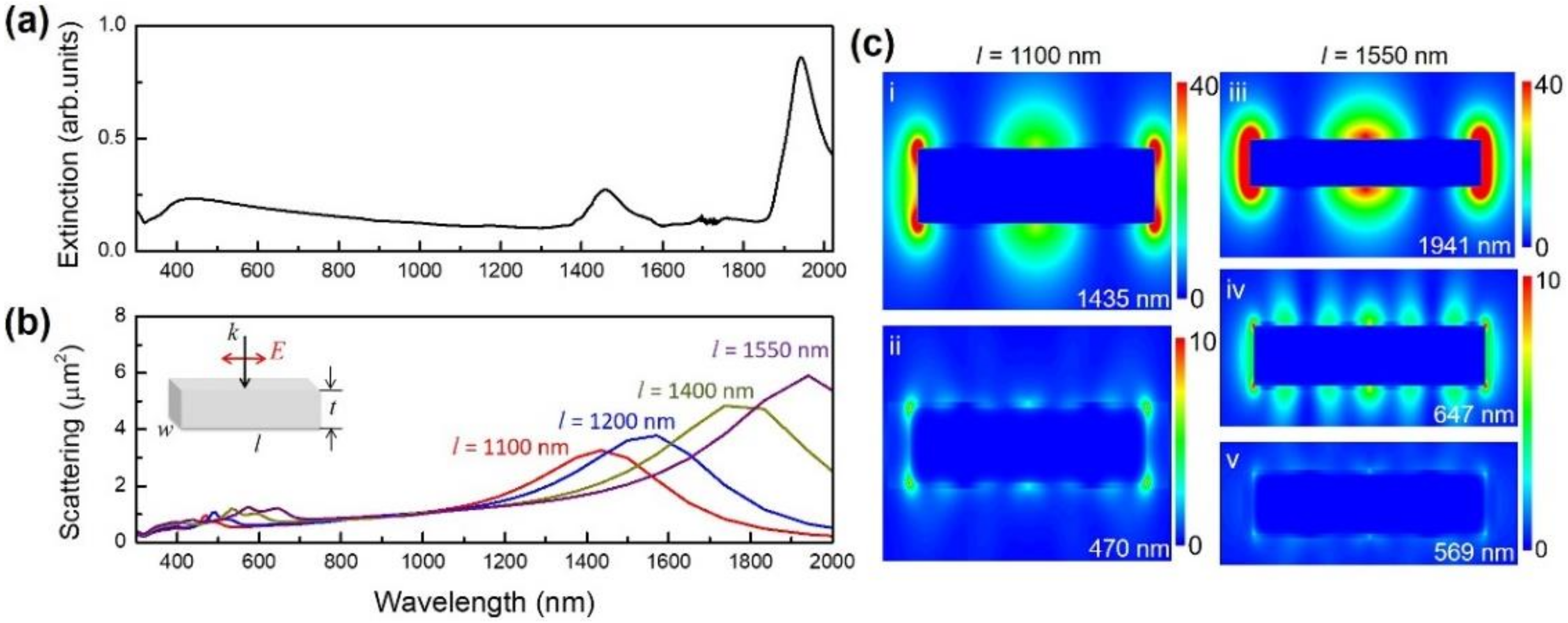
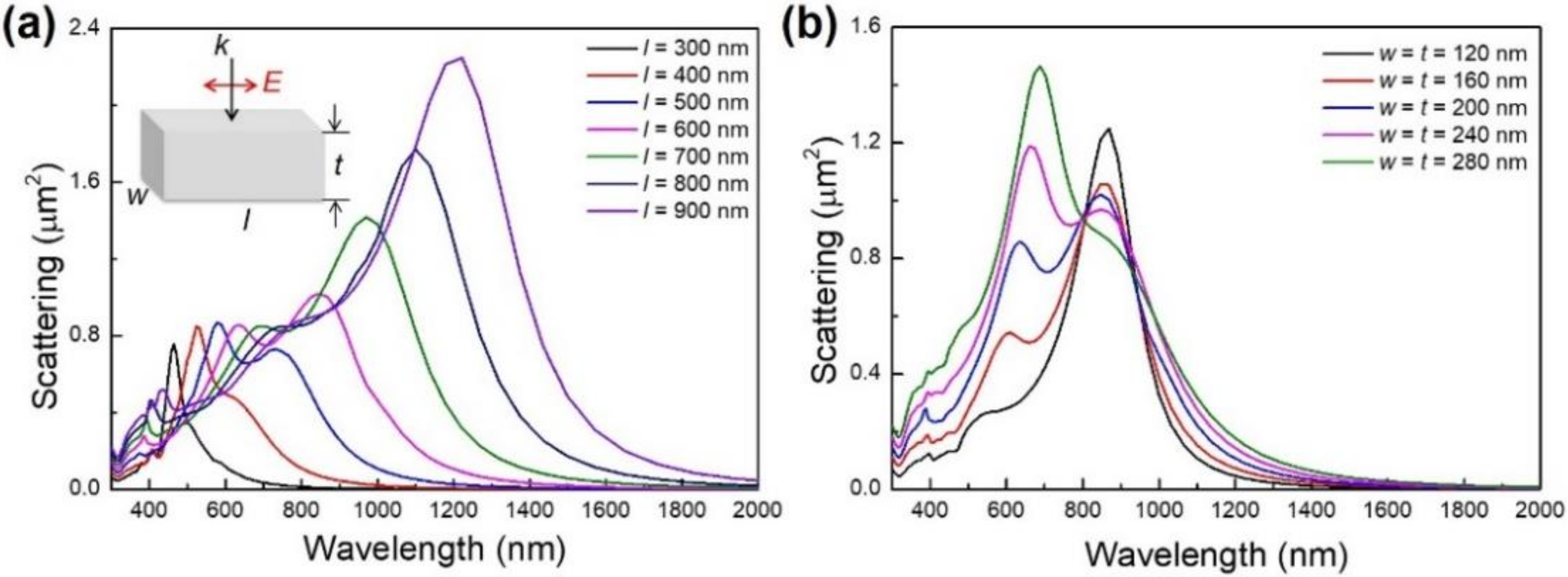
3. Results and Discussion

Figure 1a shows large-size Ag nanobars and other small Ag nanoparticles are fabricated in the polyol synthesis. The high-magnification SEM image of Ag nanobars are displayed in Figure 1b. We can see the surfaces of large-size Ag nanobars are relatively smooth with very few observed defects, as shown in Figure 1b. As demonstrated in the length distribution map in Figure 1c, the length of the Ag nanobar is 400~1360 nm.
The optical extinction spectrum of the samples containing various sizes of Ag nanobars and other Ag nanoparticles is displayed in Figure 2a. The peak located near 435 nm with broaden extinction intensities is mainly induced by the transverse resonance mode of large-size Ag nanobars and the resonance of other small Ag nanoparticles coexisting in the products. The peak originated from the longitudinal mode of the large-size Ag nanobar appears in the near-infrared wavelength range, which is obviously different from the one with the narrower size distribution [25]. Two extinction peaks in the near-infrared (NIR) wavelength range can be attributed to two kinds of nanobar aggregation formed in the extinction measurements which show different NIR responses. The longer operation wavelength (>1000 nm) of the large-size Ag nanobar widens the working wavelength of existing NIR sensing. The extinction spectrum arises from the contributions of absorption and scattering of the samples. For large nanoparticles, the extinction intensity is mainly related to the scattering of light. The differential scattering cross section relates the intensity on a single particle to the power scattered by it per solid angle [33]. The simulated scattering cross-section of a single large-size Ag nanobar is shown in Figure 2b. The optical responses of the structure are determined by the polarization of the input laser beam [34,35]. Under experimental conditions, the nanobars would be randomly oriented in the solution. Throughout simulations in this article, we set the light polarization direction parallel to the nanobar length and only multiple longitudinal plasmon modes of nanobar are excited in the spectral range of interest. The simulation results represent a specific case of the possible arrangements, which brings us a clear physical mechanism about the plasmon behavior. The LSPR peak of the Ag nanobar located at the near-infrared wavelength region shifts to red with increasing nanobar length. For a nanobar with a length of 1400 nm (close to the maximum length in the experiments), the dipole resonance appears at ~1800 nm, which is different to the results shown in Figure 2a. This discrepancy can be attributed to the coupling among nanobar aggregates in the extinction measurements that lead to the red-shifting resonant wavelength. The corresponding local electric field distribution of a single large-size nanobar (l = 1100 nm and 1550 nm, respectively) excited by the resonance wavelength (λres) is shown in Figure 2c. We can see that for the dipole resonance wavelength (see (i) and (iii)), the electric field is strongly confined in the corner and side of the nanobar, resulting in the increased scattering cross-section as displayed in Figure 2b. Moreover, higher order longitudinal modes are excited in the larger Ag nanobars with a length of 1550 nm (see (v)). The electric field distributions at resonant wavelengths are quite different due to the different surface charge distributions on Ag nanobars [36,37,38,39]. The SPRs in the visible and near-infrared region arise from the phase difference at nanobar ends and Fabry–Perot resonances of the surface guided waves occurring between the two ends of an individual Ag nanobar, respectively [40]. The red-shift of plasmon resonance wavelength with increasing nanobar length arises from the electromagnetic retardation effect [41,42].
To illustrate the size influence on the surface plasmon resonance of Ag nanobars, a series of simulations were performed on Ag nanobars with different length (l), width (w) and thickness (t). Figure 3a shows the simulated scattering cross-section of a single Ag nanobar with length varying from 300 nm to 900 nm. With increasing nanobar length, the dipole resonance is red-shifted from 465 nm to 1.2 μm, which is a broad-band range across the visible and near-infrared region. This can be attributed to the retardation effect caused by the increased nanobar length. High-order plasmon modes excited in the large-size Ag nanobars emerge in the visible light region. For a single Ag nanobar (l = 300 nm), the quadrupole plasmon mode appears at ~410 nm. When the nanobar length is above 300 nm, higher-order modes are excited. Due to the large red-shift of the dipole resonance compared with that of high-order resonance, the interaction between the dipole mode and high-order mode is weak in a large-size Ag nanobar [43]. In addition, the effect of width and thickness of the Ag nanobar (l = 600 nm) on longitudinal resonance modes have been investigated, as shown in Figure 3b. We can see with increasing nanobar width and thickness, quadrupole resonance at ~600 nm becomes distinguished as the charges decouple, while high-order resonance peak position (around 400 nm) is affected due to a small extent. The red-shifting and broadening quadrupole resonance peak is possibly due to the retardation and radiative damping effects. For the longitudinal dipole resonance, the peak location has almost no change when the nanobar length is kept constant. We thus infer that etching a large-size nanobar along nanobar length direction can broadly tune the LSPR peak.
Figure 4 shows the scattering cross-section of large-size nanobar (w = t = 200 nm, l = 700 nm) before and after the etch process. Three kinds of nanobar arrays are made by etching a large-size Ag nanobar along the length direction. Compared with the LSPR peaks in an Ag nanobar without being etched, as shown in Figure 4a, we find that the resonance wavelength has an obvious change. With an increasing number of etch times, all LSPR peaks appear at a shorter wavelength. The dipole resonance peak shifts from ~970 nm to ~450 nm by the etch process. Moreover, the scattering intensity is decreased by increasing the etch times. We simulate the scattering cross-section of an individual small bar (l = 25 nm, 50 nm, 125 nm and 150 nm, respectively) and find that the LSPR peaks appear at the visible wavelength region. When two or more small bars are placed side by side (the gap between the nanobars is 50 nm), the bonding dipole–dipole mode shifts to a longer wavelength and a new resonant peak is excited by the coupling effect of these small bars. The scattering cross-section of side-by-side nanobars far exceeds that of an individual small bar, which can be attributed to the coupling among bars resulting in the increased scattering efficiency of radiative modes [44]. In addition, the strong radiative damping introduced by in-phase oscillation of the individual small bar dipoles leads to the broad bandwidth in etched nanobars [45]. Consequently, we conclude the shift of surface plasmon resonance wavelength and change of intensity can be attributed to the coupling of plasmon modes excited in individual small bars, as the etched nanobar can be seen as the arrangement of side-by-side small nanobars. For an Ag nanobar with a larger length, the resonance wavelength is possible to be widely tuned from the visible to the near-infrared region by advanced etch technology. When the gap of side-by-side nanobars is decreased to several nanometers, the coupling effect of plasmons can enhance by generating gap plasmon resonance among small nanobars. The gap plasmon resonance modes, generally with a narrower full width at half maximum (FWHM) value, leads to a relatively high sensitivity and good figure of merit (FOM). The etch technology provides an effective approach to flexibly control the LSPR response of the large-size Ag nanobar for potential applications. It should be noted that the follow-up experiment is carrying on, and that through precisely controlling the morphology of etched nanobars, the tunable LSPR peak position change in a wide spectra range can be realized.
The RI sensing property of a large-size Ag nanobar is investigated in Figure 5. We can see from Figure 5a that the resonance wavelength of a large-size Ag nanobar red-shifts with the increase of the RI of ambient medium, which is consistent with the experimental and simulated results from other nanoparticle structures reported previously [29,46,47]. The maximum resonance wavelength and corresponding fitted curves for different RI are shown in the inset of Figure 5a. The slope of the line by definition Δλres/Δn is equal to the sensitivity (S). The FOM can be defined as FOM = S/FWHM. The RI sensitivity of Ag nanobar (w = t = 200 nm, l = 900 nm) is calculated as 1193 nm/RIU (RIU is refractive index unit), and FOM is of 3.4 RIU−1, which is comparable with that of other single metal nanoparticle for ultrasensitive nanosensors [48]. The comparison of the LSPR performance for individual nanoparticles, clusters and arrays is shown in Table 1. The broad linewidth in the scattering cross-section of a single large-size Ag nanobar limits the FOM. LSPR-based nanosensors with high sensitivity and FOM are expected to be obtained by precisely designing the nanostructures by directly etching a single large-size nanobar into small-area arrays, or self-assemble a nanobar to make large-area arrays through the lithography process. Generally, in the polyol fabrication process with PVP as a surface active agent, the surface of the Ag nanobar is coated with a thin PVP layer (thickness < 5 nm). A thin PVP layer could vary the RI surrounding nanobar. To check the influence of the PVP layer on the LSPR property of a large-size Ag nanobar, we simulated the scattering cross-section of a single nanobar with different thickness of PVP layer, as shown in Figure 5b. It can be seen that the LSPR peak red-shifts with increasing thickness of the PVP layer, which can be attributed to the low oscillation energy experienced by localized surface plasmon in an Ag nanobar with a thicker PVP layer (RI of 1.5), and thus leading to the lower resonance frequency [37,49]. For thinner PVP coating (thickness: 3 nm), there is almost no obvious effect on the LSPR properties of a nanobar. That means that the effect of a thin PVP layer on Ag nanobars synthesized by the polyol method generally can be ignored.

4. Conclusions

Large-size Ag nanobars (length: 400~1360 nm, width and thickness: 100~200 nm) working at longer wavelength (> 1000 nm) have been synthesized through a polyol process method using bromide ions. Large-size Ag nanobars show excellent tunable LSPR from visible to infrared region (400 nm~2 μm) by changing the bar size or etching bar in the length direction. By systematically studying large-size Ag nanobars through FDTD simulation, we found that the dipole resonance peak is mainly related to the length of a nanobar. Through systematic investigation of an individual nanobar, we find the plasmonic properties of etched nanobars result from the coupling effect of arranged side-by-side small nanobars. In addition, through changing the refractive index of medium around nanobars, as well as the PVP coating thickness, the plasmon resonance of a large-size Ag nanobar can also be tuned. The simulated RI sensitivity of an individual large-size Ag nanobar can reach 1193 nm/RIU, and a FOM of 3.4. This work is expected to promote the development of large-size plasmon-based nanomaterials and their applications on the fabrication of nanoparticle arrays for broad-band absorbers, sensors and nanofilters.

Author Contributions

Conceptualization, F.W. and W.W.; methodology, F.W.; software, L.C.; validation, F.W. and L.C.; formal analysis, F.W., L.C. and W.W.; writing—original draft preparation, F.W.; writing—review and editing, W.W.; project administration, W.W.; funding acquisition, F.W. and W.W. All authors have read and agreed to the published version of the manuscript.

Funding

This research was funded by the Research Fund for the Doctoral Program of Xi’an Polytechnic University (BS201904), the Science and Technology Guidance Plan Project of China Textile Industry Federation (2020003), the Open Project Program of Key Laboratory of Nanodevices and Applications (20YZ07) from the Chinese Academy of Sciences, and the National Natural Science Foundation of China (11674259).

Acknowledgments

L.C. acknowledges the financial support from the China Scholarship Council.

Conflicts of Interest

The authors declare no conflict of interest.

References

  1. Zaman, M.A.; Padhy, P.; Hesselink, L. Near-field Optical Trapping in a Non-conservative Force Field. Sci. Rep. 2019, 9, 649. [Google Scholar] [CrossRef] [PubMed]
  2. Nicoletti, O.; De la Pena, F.; Leary, R.K.; Holland, D.J.; Ducati, C.; Midgley, P.A. Three-Dimensional Imaging of Localized Surface Plasmon Resonances of Metal Nanoparticles. Nature 2013, 502, 80–84. [Google Scholar] [CrossRef] [PubMed]
  3. Kravets, V.G.; Kabashin, A.V.; Barnes, W.L.; Grigorenko, A.N. Plasmonic Surface Lattice Resonances: A Review of Properties and Applications. Chem. Rev. 2018, 118, 5912–5951. [Google Scholar] [CrossRef] [PubMed]
  4. Sobhani, F.; Heidarzadeh, H.; Bahador, H. Photocurrent Improvement of an Ultra-thin Silicon Solar Cell Using the Localized Surface Plasmonic Effect of Clustering Nanoparticles. Chin. Phys. B 2020, 29, 068401. [Google Scholar] [CrossRef]
  5. Yu, P.; Besteiro, L.V.; Huang, Y.; Wu, J.; Fu, L.; Tan, H.H.; Jagadish, C.; Wiederrecht, G.P.; Govorov, A.O.; Wang, Z. Broadband Metamaterial Absorbers. Adv. Opt. Mater. 2018, 7, 1800995. [Google Scholar] [CrossRef] [Green Version]
  6. Ueno, K.; Oshikiri, T.; Misawa, H. Plasmon-Induced Water Splitting Using Metallic-Nanoparticle-Loaded Photocatalysts and Photoelectrodes. Chemphyschem 2016, 17, 199–215. [Google Scholar] [CrossRef] [PubMed]
  7. Zhang, P.; Wang, T.; Gong, J. Mechanistic Understanding of the Plasmonic Enhancement for Solar Water Splitting. Adv. Mater. 2015, 27, 5328–5342. [Google Scholar] [CrossRef]
  8. Lednicky, T.; Bonyar, A. Large Scale Fabrication of Ordered Gold Nanoparticle-Epoxy Surface Nanocomposites and Their Application as Label-Free Plasmonic DNA Biosensors. ACS Appl. Mater. Interfaces 2020, 12, 4804–4814. [Google Scholar] [CrossRef]
  9. Danilov, A.; Tselikov, G.; Wu, F.; Kravets, V.G.; Ozerov, I.; Bedu, F.; Grigorenko, A.N.; Kabashin, A.V. Ultra-Narrow Surface Lattice Resonances in Plasmonic Metamaterial Arrays for Biosensing Applications. Biosens. Bioelectron. 2018, 104, 102–112. [Google Scholar] [CrossRef] [Green Version]
  10. Zheng, P.; Tang, H.; Liu, B.; Kasani, S.; Huang, L.; Wu, N. Origin of Strong and Narrow Localized Surface Plasmon Resonance of Copper Nanocubes. Nano Res. 2018, 12, 63–68. [Google Scholar] [CrossRef]
  11. Wu, F.; Wang, W.; Xu, Z.; Li, F. Bromide (Br)-Based Synthesis of Ag Nanocubes with High-Yield. Sci. Rep. 2015, 5, 10772. [Google Scholar] [CrossRef] [PubMed]
  12. Tan, T.; Tian, C.; Ren, Z.; Yang, J.; Chen, Y.; Sun, L.; Li, Z.; Wu, A.; Yin, J.; Fu, H. LSPR-Dependent SERS Performance of Silver Nanoplates with Highly Stable and Broad Tunable LSPRs Prepared through an Improved Seed-Mediated Strategy. Phys. Chem. Chem. Phys. 2013, 15, 21034–21042. [Google Scholar] [CrossRef] [PubMed]
  13. Ghosh, P.K.; Debu, D.T.; French, D.A.; Herzog, J.B. Calculated Thickness Dependent Plasmonic Properties of Gold Nanobars in the Visible to near-Infrared Light Regime. PLoS ONE 2017, 12, e0177463. [Google Scholar] [CrossRef]
  14. Chen, Y. Nanofabrication by Electron Beam Lithography and Its Applications: A Review. Microelectron. Eng. 2015, 135, 57–72. [Google Scholar] [CrossRef]
  15. Shi, X.; Verschueren, D.; Pud, S.; Dekker, C. Integrating Sub-3 nm Plasmonic Gaps into Solid-State Nanopores. Small 2018, 14, e1703307. [Google Scholar] [CrossRef]
  16. Gu, P.; Zhang, W.; Zhang, G. Plasmonic Nanogaps: From Fabrications to Optical Applications. Adv. Mater. Interfaces 2018, 5, 1800648. [Google Scholar] [CrossRef]
  17. Cordoba, R.; Orus, P.; Strohauer, S.; Torres, T.E.; De Teresa, J.M. Ultra-Fast Direct Growth of Metallic Micro- and Nano-Structures by Focused Ion Beam Irradiation. Sci. Rep. 2019, 9, 14076. [Google Scholar] [CrossRef] [Green Version]
  18. Michaeli, L.; Keren-Zur, S.; Avayu, O.; Suchowski, H.; Ellenbogen, T. Nonlinear Surface Lattice Resonance in Plasmonic Nanoparticle Arrays. Phys. Rev. Lett. 2017, 118, 243904. [Google Scholar] [CrossRef]
  19. Sanchez-Esquivel, H.; Raygoza-Sanchez, K.Y.; Rangel-Rojo, R.; Kalinic, B.; Michieli, N.; Cesca, T.; Mattei, G. Ultra-Fast Dynamics in the Nonlinear Optical Response of Silver Nanoprism Ordered Arrays. Nanoscale 2018, 10, 5182–5190. [Google Scholar] [CrossRef]
  20. Wang, X.; Zhu, J.; Tong, H.; Yang, X.; Wu, X.; Pang, Z.; Yang, H.; Qi, Y. A Theoretical Study of a Plasmonic Sensor Comprising a Gold Nano-Disk Array on Gold Film with a SiO2 Spacer. Chin. Phys. B 2019, 28, 044201. [Google Scholar] [CrossRef]
  21. Singh, P. SPR Biosensors: Historical Perspectives and Current Challenges. Sens. Actuators B Chem. 2016, 229, 110–130. [Google Scholar] [CrossRef]
  22. Zhou, S.; Mesina, D.S.; Organt, M.A.; Yang, T.-H.; Yang, X.; Huo, D.; Zhao, M.; Xia, Y. Site-Selective Growth of Ag Nanocubes for Sharpening Their Corners and Edges, Followed by Elongation into Nanobars through Symmetry Reduction. J. Mater. Chem. C 2018, 6, 1384–1392. [Google Scholar] [CrossRef]
  23. Tuersun, P. Simulated Localized Surface Plasmon Spectra of Single Gold and Silver Nanobars. Optik 2016, 127, 3466–3470. [Google Scholar] [CrossRef]
  24. Wiley, B.J.; Chen, Y.; McLellan, J.M.; Xiong, Y.; Li, Z.; Ginger, D.; Xia, Y. Synthesis and Optical Properties of Silver Nanobars and Nanorice. Nano Lett. 2007, 7, 1032–1036. [Google Scholar] [CrossRef] [PubMed]
  25. Zhang, Q.; Moran, C.H.; Xia, X.; Rycenga, M.; Li, N.; Xia, Y. Synthesis of Ag Nanobars in the Presence of Single-Crystal Seeds and a Bromide Compound, and Their Surface-Enhanced Raman Scattering (SERS) Properties. Langmuir 2012, 28, 9047–9054. [Google Scholar] [CrossRef]
  26. Hu, X.L.; Sun, L.B.; Shi, B.; Ye, M.; Xu, Y.; Wang, L.S.; Zhao, J.; Li, X.L.; Wu, Y.Q.; Yang, S.M.; et al. Influence of Film Thickness and Nanograting Period on Color-Filter Behaviors of Plasmonic Metal Ag Films. J. Appl. Phys. 2014, 115, 113104. [Google Scholar] [CrossRef]
  27. Dong, J.; Cao, Y.; Han, Q.; Gao, W.; Li, T.; Qi, J. Nanoscale Flexible Ag Grating/AuNPs Self-Assembly Hybrid for Ultra-Sensitive Sensors. Nanotechnology 2021, 32, 155603. [Google Scholar] [CrossRef]
  28. Gnilitskyi, I.; Mamykin, S.V.; Lanara, C.; Hevko, I.; Dusheyko, M.; Bellucci, S.; Stratakis, E. Laser Nanostructuring for Diffraction Grating Based Surface Plasmon-Resonance Sensors. Nanomaterials 2021, 11, 591. [Google Scholar] [CrossRef]
  29. Li, G.; Hu, H.; Wu, L. Tailoring Fano Lineshapes Using Plasmonic Nanobars for Highly Sensitive Sensing and Directional Emission. Phys. Chem. Chem. Phys. 2018, 21, 252–259. [Google Scholar] [CrossRef]
  30. Si, G.Y.; Leong, E.S.; Pan, W.; Chum, C.C.; Liu, Y.J. Plasmon-Induced Transparency in Coupled Triangle-Rod Arrays. Nanotechnology 2015, 26, 025201. [Google Scholar] [CrossRef]
  31. Chen, H.-Y.; He, C.-L.; Wang, C.-Y.; Lin, M.-H.; Mitsui, D.; Eguchi, M.; Teranishi, T.; Gwo, S. Far-Field Optical Imaging of a Linear Array of Coupled Gold Nanocubes: Direct Visualization of Dark Plasmon Propagating Modes. ACS Nano 2011, 5, 8223–8229. [Google Scholar] [CrossRef] [PubMed]
  32. Palik, E.D. Handbook of Optical Constants of Solids; Academic Press: Orlando, FL, USA, 1985. [Google Scholar]
  33. Kim, J.H.; Ehrman, S.H.; Mulholland, G.W.; Germer, T.A. Polarized Light Scattering by Dielectric and Metallic Spheres on Silicon Wafers. Appl. Opt. 2002, 41, 5405–5412. [Google Scholar] [CrossRef] [PubMed]
  34. Wang, K.; Schonbrun, E.; Steinvurzel, P.; Crozier, K.B. Trapping and Rotating Nanoparticles Using a Plasmonic Nano-tweezer with an Integrated Heat Sink. Nat. Commun. 2011, 2, 469. [Google Scholar] [CrossRef] [Green Version]
  35. Zaman, M.A.; Padhy, P.; Hesselink, L. Solenoidal Optical Forces from a Plasmonic Archimedean Spiral. Phys. Rev. A 2019, 100, 013857. [Google Scholar] [CrossRef] [PubMed]
  36. Chou Chau, Y.F.; Chou Chao, C.T.; Huang, H.J.; Kooh, M.R.R.; Kumara, N.T.R.N.; Lim, C.M.; Chiang, H.P. Perfect Dual-Band Absorber Based on Plasmonic Effect with the Cross-Hair/Nanorod Combination. Nanomaterials 2020, 10, 493. [Google Scholar] [CrossRef] [PubMed] [Green Version]
  37. Chou Chau, Y.F.; Chou Chao, C.T.; Rao, J.Y.; Chiang, H.P.; Lim, C.M.; Lim, R.C.; Voo, N.Y. Tunable Optical Performances on a Periodic Array of Plasmonic Bowtie Nanoantennas with Hollow Cavities. Nanoscale Res. Lett. 2016, 11, 411. [Google Scholar] [CrossRef] [Green Version]
  38. Chou Chau, Y.F.; Chou Chao, C.T.; Huang, H.J.; Anwar, U.; Lim, C.M.; Voo, N.Y.; Mahadi, A.H.; Kumara, N.T.R.N.; Chiang, H.-P. Plasmonic Perfect Absorber Based on Metal Nanorod Arrays Connected with Veins. Results Phys. 2019, 15, 102567. [Google Scholar] [CrossRef]
  39. Chou Chau, Y.F.; Lee, C.M.; Lee, C.; Huang, H.J.; Lin, C.-T.; Kumara, N.T.R.N.; Yoong, V.N.; Chiang, H.P. Tailoring Surface Plasmon Resonance and Dipole Cavity Plasmon Modes of Scattering Cross Section Spectra on the Single Solid-Gold/Gold-Shell Nanorod. J. Appl. Phys. 2016, 120, 093110. [Google Scholar] [CrossRef]
  40. Chou Chau, Y.F. Intriguing Standing Wave Numbers and Plasmonic Effects on the Solid-Metal/Metal-Shell Nanorod Surface. Plasmonics 2017, 12, 277–285. [Google Scholar] [CrossRef]
  41. Sönnichsen, C.; Franzl, T.; Wilk, T.; Plessen, G.; Feldmann, J. Plasmon Resonances in Large Noble-Metal Clusters. New J. Phys. 2002, 4, 93. [Google Scholar] [CrossRef] [Green Version]
  42. Hartland, G.V. Optical Studies of Dynamics in Noble Metal Nanostructures. Chem. Rev. 2011, 111, 3858–3887. [Google Scholar] [CrossRef] [PubMed]
  43. Chen, J.; Xiang, J.; Jiang, S.; Dai, Q.; Tie, S.; Lan, S. Multipole Radiations from Large Gold Nanospheres Excited by Evanescent Wave. Nanomaterials 2019, 9, 175. [Google Scholar] [CrossRef] [Green Version]
  44. Chen, S.-Y.; Mock, J.J.; Hill, R.T.; Chilkoti, A.; Smith, D.R.; Lazarides, A.A. Gold Nanoparticles on Polarizable Surfaces as Raman Scattering Antennas. ACS Nano 2010, 4, 6535–6546. [Google Scholar] [CrossRef] [PubMed] [Green Version]
  45. Mirin, N.A.; Bao, K.; Nordlander, P. Fano Resonances in Plasmonic Nanoparticle Aggregates. J. Phys. Chem. A 2009, 113, 4028–4034. [Google Scholar] [CrossRef] [PubMed]
  46. McFarland, A.D.; Van Duyne, R.P. Single Silver Nanoparticles as Real-Time Optical Sensors with Zeptomole Sensitivity. Nano Lett. 2003, 3, 1057–1062. [Google Scholar] [CrossRef] [Green Version]
  47. Sherry, L.J.; Chang, S.-H.; Schatz, G.C.; Van Duyne, R.P. Localized Surface Plasmon Resonance Spectroscopy of Single Silver Nanocubes. Nano Lett. 2005, 5, 2034–2038. [Google Scholar] [CrossRef] [PubMed]
  48. Chen, W.; Hu, H.; Jiang, W.; Xu, Y.; Zhang, S.; Xu, H. Ultrasensitive Nanosensors Based on Localized Surface Plasmon Resonances: From Theory to Applications. Chin. Phys. B 2018, 27, 107403. [Google Scholar] [CrossRef]
  49. Kumara, N.T.R.N.; Chou Chau, Y.F.; Huang, J.W.; Huang, H.J.; Lin, C.-T.; Chiang, H.P. Plasmonic Spectrum on 1D and 2D Periodic Arrays of Rod-Shape Metal Nanoparticle Pairs with Different Core Patterns for Biosensor and Solar Cell Applications. J. Opt. 2016, 18, 115003. [Google Scholar] [CrossRef]
  50. Julien Burgin, M.L.; Philippe, G.-S. Dielectric Sensing with Deposited Gold Bipyramids. J. Phys. Chem. C 2008, 112, 19279–19282. [Google Scholar] [CrossRef]
  51. Lassiter, J.B.; Sobhani, H.; Fan, J.A.; Kundu, J.; Capasso, F.; Nordlander, P.; Halas, N.J. Fano Resonances in Plasmonic Nanoclusters: Geometrical and Chemical Tunability. Nano Lett. 2010, 10, 3184–3189. [Google Scholar] [CrossRef]
  52. Ye, J.; Van Dorpe, P. Improvement of Figure of Merit for Gold Nanobar Array Plasmonic Sensors. Plasmonics 2011, 6, 665–671. [Google Scholar] [CrossRef]
Figure 1. The characterization of large-size Ag nanobar. (a) Scanning electron microscope (SEM) image of Ag nanobars. (b) The high-magnification SEM image of Ag nanobars. (c) The length distribution map of Ag nanobars.
Micromachines 13 00638 g001
Figure 2. The localized surface plasmon resonance (LSPR) properties of a large-size Ag nanobar. (a) The experimental extinction spectrum taken from aqueous suspension of silver nanobars with various sizes. (b) The simulated scattering cross-section of two large-size silver nanobars (w = t = 200 nm, l = 1100 nm, 1200 nm, 1400 nm and 1550 nm, respectively) at an incident angle (θ = 0°) in air (RI = 1.0). (c) The corresponding electric field distributions for a nanobar (w = t = 200 nm) with two different lengths at on-resonance wavelengths (i) l = 1100 nm, λres = 1435 nm, (ii) l = 1100 nm, λres = 470 nm, (iii) l = 1550 nm, λres = 1941 nm, (iv) l = 1550 nm, λres = 647 nm, and (v) l = 1550 nm, λres = 569 nm.
Micromachines 13 00638 g002
Figure 3. Finite-difference time-domain (FDTD) simulated scattering cross-section of single silver nanobar with various sizes at an incident angle (θ = 0°) in air (RI = 1.0). (a) Width and thickness (w = t = 200 nm) and lengths (l = 300 nm, 400 nm, 500 nm, 600 nm, 700 nm, 800 nm and 900 nm, respectively). (b) Length (l = 600 nm), width and thickness (w = t = 120 nm, 160 nm, 200 nm, 240 nm and 280 nm, respectively).
Micromachines 13 00638 g003
Figure 4. The LSPR property of a large-size Ag nanobar (w = t = 200 nm, l = 700 nm) before and after being etched along the length direction. (a) The simulated scattering cross-section of an original large-size Ag nanobar and (bd) three etched nanostructures (black solid lines), individual nanobars (red and blue dashed lines) and the coupling effect of small-size nanobars (other colored dashed lines) simulated at an incident angle (θ = 0°) in air (RI = 1.0). The insets show the corresponding schematic diagrams of a large-size Ag nanobar before and after the etch process. The width and thickness of each etch in white is 200 nm and the length is 50 nm.
Micromachines 13 00638 g004
Figure 5. The influence of ambient medium and polyvinylpyrrolidone (PVP) coating on the surface plasmon resonance of a large-size Ag nanobar. (a) The simulated scattering cross-section of a single silver nanobar (l = 900 nm, w = t = 200 nm) in different ambient medium with various refractive indexes (RI = 1.0, 1.1, 1.2, 1.3, 1.4, 1.5) at an incident angle (θ = 0°). The inset shows the relationships between maximum resonance wavelength with the refractive index of the surrounding medium. (b) The simulated scattering cross-section of a single silver nanobar (l = 900 nm, w = t = 200 nm) with different thicknesses of PVP coating. The thickness of the PVP layer is 3 nm, 9 nm, 27 nm, 60 nm and 100 nm, respectively.
Micromachines 13 00638 g005
Table 1. LSPR sensitivities for nanostructures used in the experiments and simulations.
NanostructureSensitivity (nm/RIU)FOM (RIU−1)TypeReference
Rodlike Ag nanoparticle2354.1experiment[46]
Ag nanobar11933.4simulationthis work
Ag nanocube15655.4experiment[47]
Au bipyramids20004.5experiment[50]
Au nanodisk heptamer23405.4experiment[51]
Au heptamer94020.9simulation[29]
Ag sphere septamer51510.6simulation[45]
Au nanobar array6004.68simulation[52]
Au nanodisk array853126simulation[20]
Cross-hair/nanorod combination120026.67simulation[36]
Ag nanorod arrays with the connected veins80012.17simulation[38]
Publisher’s Note: MDPI stays neutral with regard to jurisdictional claims in published maps and institutional affiliations.

