Article

A Novel AlGaN/Si3N4 Compound Buffer Layer HEMT with Improved Breakdown Performances

1
Chongqing Engineering Laboratory of High Performance Integrated Circuits, School of Microelectronics and Communication Engineering, Chongqing University, Chongqing 400044, China
2
China Resources Microelectronics (Chongqing) Limited, Chongqing 401332, China
*
Author to whom correspondence should be addressed.
Micromachines 2022, 13(3), 464; https://doi.org/10.3390/mi13030464
Submission received: 12 February 2022 / Revised: 10 March 2022 / Accepted: 14 March 2022 / Published: 18 March 2022

Abstract

:
In this article, an AlGaN and Si3N4 compound buffer layer high electron mobility transistor (HEMT) is proposed and analyzed through TCAD simulations. In the proposed HEMT, the Si3N4 insulating layer is partially buried between the AlGaN buffer layer and AlN nucleating layer, which introduces a high electric field from the vertical field plate into the internal buffer region of the device. The compound buffer layer can significantly increase the breakdown performance without sacrificing any dynamic characteristics and increasing the difficulty in the fabrication process. The significant structural parameters are optimized and analyzed. The simulation results reveal that the proposed HEMT with a 6 μm gate-drain distance shows an OFF-state breakdown voltage (BV) of 881 V and a specific ON-state resistance (Ron,sp) of 3.27 mΩ·cm2. When compared with the conventional field plate HEMT and drain connected field plate HEMT, the breakdown voltage could be increased by 148% and 94%, respectively.

1. Introduction

Gallium nitride (GaN) devices are widely used in the high-frequency and high-power fields of power electronics due to their superior material properties, such as a large band gap, high critical electric field, good thermal conductivity, and high electron saturation speed [1,2,3,4,5]. AlGaN/GaN high electron mobility transistor (HEMT) devices are fabricated by growing a thin AlGaN barrier layer on the GaN channel layer based on a transition layer [6,7]. The strong polarization effect between AlGaN and GaN will confine the electrons at the surface of the GaN channel, thereby forming a 2-dimensional electron gas (2DEG) with high mobility [8,9]. At the same time, GaN-on-silicon is widely used owing to its low cost and large size, which can be integrated with Si-CMOS technology [10,11]. In recent years, there have been an increasing number of reports on high-performance AlGaN/GaN HEMT devices [12,13,14,15,16,17], however, there is still a large gap between the limits of GaN material properties and commercial devices. Researchers mainly use field plate technology or progressive transition layers to obtain a low specific on-resistance (Ron,sp) with a high breakdown voltage (BV), thereby realizing a higher figure-of-merits (FOM) (FOM = BV2/Ron,sp). The field plate is capable of alleviating the electrical field crowding at the drain side of the gate edge. At the same time, the field plate introduces a new electrical field peak at its edge, which has been proven to significantly improve the BV [18,19,20]. In the fabrication process, the field plate is connected to the gate and placed over the passivation layer. However, the improvement of the device performance depends on the lateral length of the field plate, and the breakdown voltage rises at the beginning and then declines with increasing field plate [11,12,13,14,15,16,17,18,19,20,21]. At the same time, the field plate is equivalent to increasing the electrode overlapping area, which brings the corresponding parasitic capacitance and deteriorates the switching performance of the device. Recently, an AlGaN or GaN buffer layer is substituted by an AlN back barrier layer that has been fabricated and demonstrated to have a high BV and FOM [22,23,24]. Utilizing the characteristics of AlN with an ultra-large bandgap energy (6.2 eV) and polarization effect, the confinement effect of 2DEG is increased. Therefore, a higher BV and a lower Ron,sp can be obtained. However, GaN HEMTs with an AlN back barrier architecture will introduce a negative bound charge between the GaN and AlN, which will deplete the channel 2DEG, reduce the channel electron density, and exacerbate the output performance [25]. On the other hand, the interface of the AlN and silicon substrate will form the inversion electron layer in the buffer region, which will increase the leakage of the device and block the expansion of the depletion layer, thus affecting the breakdown characteristics [26]. To eliminate these adverse effects, the AlN layer needs to be meticulously designed and optimized, which will undoubtedly increase the cost and process complexity.
Recently, a novel drain-connected field plate GaN HEMT (DC-HEMT) was proposed, which improved the breakdown and radio frequency power amplifier performance by taking advantage of a vertical-field plate [21]. However, the withstand voltage in the buffer region remains limited. Therefore, this paper proposes a novel high-performance HEMT with a compound buffer layer, which changes the conventional AlGaN or GaN buffer layer into an AlGaN and Si3N4 compound buffer layer. On the basis of adopting the vertical drain field plate structure, a high electric field on the device surface is introduced into the buffer region. At the same time, the compound buffer layer increases the insulation and reduces the buffer leakage. In this paper, the internal mechanism of the device structure is comprehensively analyzed by numerical simulation, and the parameters of the device are optimized. Finally, the optimized proposed HEMT obtains a BV of 881 V and a Ron,sp of 3.27 mΩ·cm2 at a gate drain distance (LGD) of 6 μm. This paper is arranged as follows. The second chapter introduces the structure and mechanism analysis of the proposed method. Then, the third chapter presents the simulation results and optimizes the important parameters. Finally, the last chapter provides a conclusion.

2. Device Structure and Mechanism

The schematic cross-section of the proposed buried Si3N4 passivation layer GaN HEMT (BP-HEMT) is shown in Figure 1c. For comparison, the conventional drain field plate HEMT (Con-HEMT) and DC-HEMT are given in Figure 1a,b, respectively. One available fabricating process flow of the proposed GaN HEMT is introduced as summarized below. Firstly, A 50 nm AlN nucleation layer is grown by metal-organic chemical vapor deposition (MOCVD) on a 3 μm n-type silicon substrate. Secondly, the buried Si3N4 layer is grown at high temperature in the same MOCVD chamber with silane and ammonia. Then, the Si3N4 layer under the source side is removed selectively by using reactive ion etching (RIE) and inductively coupled plasma (ICP) etch. After that, the low-k benzocyclobutene (BCB) planarization is used to avoid the roughness between the Si3N4 and AlGaN. Finally, the epilayers and AlGaN/GaN heterojunction are regrown as the common GaN HEMTs [27,28,29]. All studied HEMTs consist of a 0.2-μm passivation layer on a 15 nm Al0.23GaN barrier layer, a 200-nm GaN channel, a 2 μm silicon-doped Al0.05GaN buffer layer.
In this study, the internal mechanism of HEMTs is simulated and analyzed by TCAD Sentaurus software from Synopsys Inc. (Mountain View, CA, USA) [30]. The drain and source electrodes are set to ohmic contacts. For the P-type GaN gate electrode, it is set to a Schottky contact. A thermal contact is set for the bulk electrode under the substrate. The necessary physical models are considered in the simulation, including the piezoelectric polarization model, anisotropy of materials, Shockley–Read–Hall (SRH) recombination model, avalanche model, mobility model considering doping-dependent degradation and high electric field velocity saturation, carrier tunneling model, and no band gap narrowing model. The electron states of the 2DEG are computed by using the model of spontaneous and piezoelectric. The 2DEG density is calculated based on the AlGaN barrier mole fraction and the strain resulting from the lattice constant. The van Dort model is as the quantization model in simulations because it is a numerically robust, fast, and proven model. The electron–electron interaction in the 2DEG is considered in the recombination and mobility models. The significant incomplete ionization of Mg ions in GaN is also considered. Figure 2 compares the experimental results from Oliver Hilt [31] and simulation results when the device is on state at VGS = 1, 3, 5 V and LGD = 6 μm. These models added in the simulations are adopted according to [32,33]. As shown in Figure 2, the IDS-VDS simulation characteristics fit well with experimental results. The Ron,sp also evidently indicates a good agreement between simulated and experimental data. A fixed acceptor trap concentration of 1 × 1018 cm−3 and a fixed donor trap concentration of 1 × 1013 cm−2 between the AlGaN barrier layer and passivation layer are equipped simultaneously [34,35]. The lateral dimensions and other doping characteristics of the devices are given in Table 1.
Figure 3 compares the lateral electric field profile at the (a) channel, cutline C1 in Figure 3c and (b) the interface between the AlGaN buffer layer and Si3N4 buried layer, cutline C2 in Figure 3c when the devices have avalanche-induced breakdown in the off state (the criteria are set when the drain current reaches 0.01 mA/mm). The electrostatic potential distribution of the proposed HEMT is also shown in Figure 3c. Comparing Figure 3a,b, it can be seen that the maximum electric field peak of the Con-HEMT is located at the edge of the drain field plate, and the electric field in the buffer region is smaller. For DC and BP HEMTs, they have not only the lateral field plates but also vertical field plates. The vertical field plate transports the high electric field into the buffer region, with the additional high electric field far away from the channel assisting in suppressing the impact ionization. Consequently, the crowded electric field at the drain electrode and field plate is alleviated, and the breakdown voltage is enlarged. In BP-HEMT, the inserted Si3N4 layer could sustain a larger electric field due to its larger band gap. It takes along the high electric field at the vertical field plate into the interior of the buffer region and therefore further enhances the electric field at the channel and the interface contrast with the DC-HEMT, as shown in Figure 3a,b. Figure 4 demonstrates the 2-D electric field distribution in the whole buffer region of (a) BP-HEMT and (b) DC-HEMT, and the electric field corresponding to the Si3N4 buried layer in the buffer region of BP-HEMT is greater than that in the single AlGaN buffer region of DC-HEMT. In summary, the novel proposed BP-HEMT employs a Si3N4 buried layer to further introduce a high electric field into the buffer region, which improves the breakdown performance without sacrificing the on-state performance.

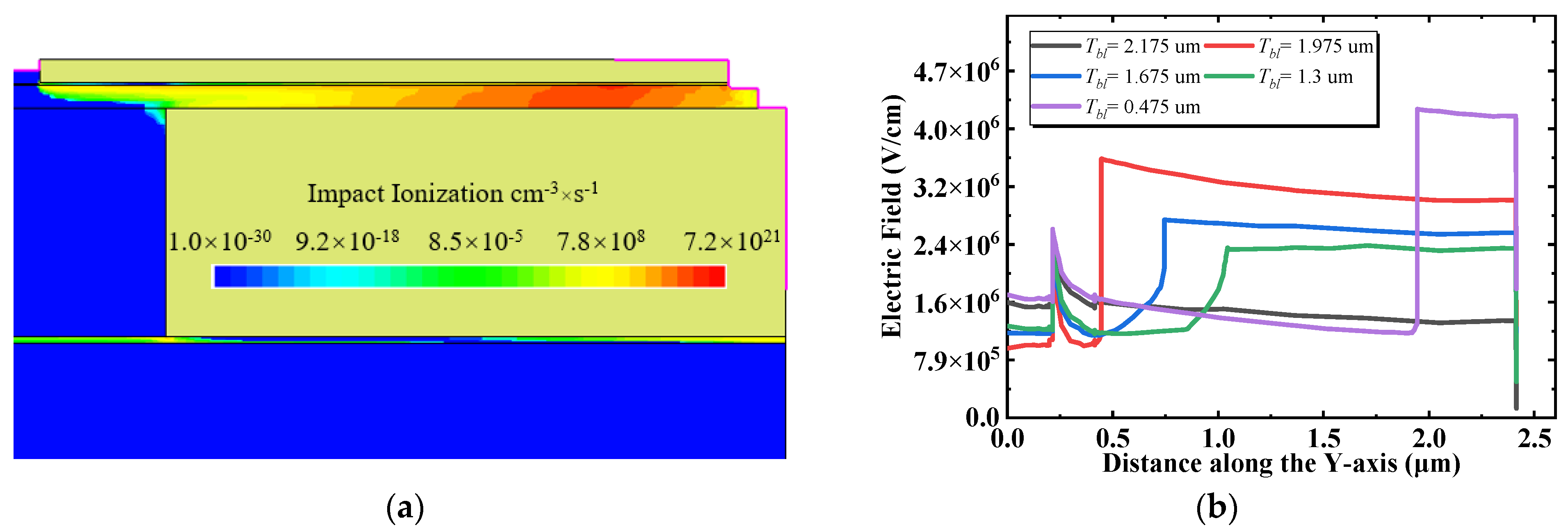
3. Simulation Results and Discussion

The breakdown characteristics of the devices are compared in Figure 5a. The breakdown voltages are 355, 454, and 881 V for Con, DC and the proposed BP-HEMTs, respectively. Compared with Con and DC-HEMTs, the BV of BP-HEMT is improved by 148% and 94%, respectively. The transfer and transconductance (defined as the calculated derivative of drain current with respect to gate-source voltage, dIDS/dVGS) of BP-HEMT are simulated at VDS = 15 V, and the gate voltage sweeps from −2 to 7 V. As shown in Figure 5b, the threshold voltage is 1.7 V, and the maximum transconductance is 0.062 S/mm. Figure 5c shows the on-state ID-VD characteristics of BP-HEMT with drain-to-source voltages that range from 0 to 18 V at VGS = 1, 3, 5, and 7 V. The current collapse phenomenon occurs when VGS > 3 V and occurs similarly in Con and DC HEMTs. The reason for the current collapse is that the electrons in the channel will be injected into the adjacent AlGaN barrier region and captured by deep traps as the VDS increases. The specific on-state resistance is 3.27 mΩ·cm2 for BP-HEMT and an approximate value for Con and DC HEMTs because the buried Si3N4 layer has no influence on the output current. Figure 5d shows the switching characteristics of the BP-HEMT when a double pulse is applied at a supply voltage of 200 V. The high-speed switching performance is preserved in the BP-HEMT.
Figure 6 shows the influence of Lbl (the length of the buried layer) on the BV and FOM of the BP-HEMT. The BV and FOM initially increase and then decrease while the Lbl rises, and the maximum values are observed to be Lbl = 5.4 μm. For further investigations, Figure 7a illustrates the off-state lateral electric field distribution at the interface between the Si3N4 buried layer and AlGaN buffer layer under a drain voltage of 500 V with different Lbl. In every single profile, the left electric field of the peak is sustained by the AlGaN buffer region, and the right electric field is maintained by Si3N4. It is apparent that the electric field in Si3N4 is higher than that in AlGaN. On the other hand, in the interior of the Si3N4 layer, the magnitude of the electric field declines progressively from the vertical field plate to the center of the buffer region. Therefore, when Si3N4 is shorter, the length of the high electric field is extremely small, and when Si3N4 is longer, nevertheless, the average electric field in the Si3N4 buried layer has a declining trend. Figure 7b calculates the integration of the electric field of Figure 7a, and the integral voltage means the magnitude of the supposed voltage in this interface. The maximum integral voltage is obtained when Lbl = 5.4 μm, and the minimum value is attained when Lbl = 1.4 μm. Moreover, the calculated integral voltages in Figure 7b that correspond to Lbl are in perfect agreement with the BV, as shown in Figure 6. In summary, Lbl has a significant effect on the average electric field. Furthermore, the supposed voltage in the buffer layer is altered. However, it should be noted that the maximum integral voltage is not equal to the drain bias voltage of the device because the total voltage is supported by lateral and vertical electric field and it is only used to compare the magnitude of the voltage assumed in the interface with different Lbl. In the on state, because the Si3N4 buried layer hardly affects the concentration and mobility of 2DEG, Ron,sp is not determined by Lbl accordingly. Lbl only slightly affects the magnitude of the saturation output current, which can be neglected.
Figure 8 shows the variation in Tbl (the thickness of the buried layer) on the BV and FOM of the proposed BP-HEMT. Apparently, BV and FOM first increased and then decreased as Tbl increased. When Tbl reaches 1.675 μm, BV and FOM reach maxima of 1098 V and 0.37 GW/cm2, respectively. Additionally, as mentioned previously, when analyzing Lbl, Ron,sp is almost independent of the Si3N4 buried layer. Therefore, the following analyses concentrate on the BV as influenced by Tbl.
Figure 9a shows the vertical electric field distribution at the location of x = 7.9 μm in the off state with a drain voltage of 700 V, and Tbl ranges from 0.475 to 2.175 μm. It should be noted that the region beneath the buffer layer does not sustain the reverse voltage. Therefore, the electric field in the substrate layer is not displayed. The electric field in the Si3N4 layer is higher than that in the AlGaN buffer region and an electric field peak is introduced at the interface between the AlGaN and Si3N4 buried layers. When the Si3N4 layer is thin (Tbl = 0.475 μm), the electric field peak neighbors the vertical field plate and is farther from the horizontal field plate and the drain electrode, and thus, it has the highest electric field peak, but the width with a high electric field is the narrowest, which equals Tbl. As the thickness of the Si3N4 layer increases, the distance from the high electric field produced by the vertical field plate is far removed. At the same time, the distance from the horizontal field plate and the drain electrode is adjacent, and the electric field peak consequently increases. The width of the high electric field also increases. Since the electric field peak at the horizontal field plate is smaller than the vertical field plate, the interface electric field peak caused by the horizontal field plate is also small. For that reason, the strength of the average electric field depends on both the width and height of the high electric field, and it rises first and reduces later, along with a similar trend in the BV and FOM. On the other hand, when the Si3N4 layer is sufficiently thick and close to the 2DEG, the high electric field will accelerate the carriers in the channel, promoting the occurrence of avalanche ionization and consequently reducing BV. Figure 9b demonstrates the impact ionization rate under a drain voltage of 700 V in the off state at Tbl = 2.175 μm. The thicker Si3N4 layer confines the impact ionization in the channel, and it brings about a premature breakdown. The above two reasons cause the BV and FOM to decrease after an initial increase.
The SiNx passivation layer on the surface of the device is widely utilized to suppress the current collapse, and the interface states between the SiNx and AlGaN barrier layers have been broadly investigated [32,33,34,35]. The existence of donor-type traps between the interface has been demonstrated, and in the proposed BP-HEMT, donor-type traps are introduced correspondingly at the interface between the AlGaN buffer and Si3N4 buried layer during fabrication. To further analyze the effect of interfacial donor traps on the breakdown performance of the device, a fixed energy level interfacial donor trap is set between the SiNx and AlGaN simultaneously during the simulation. Figure 10a shows the dependence of BV and FOM on the interface trap concentration (Ntrap) of the AlGaN buffer region and Si3N4 buried layer. The BV and FOM increase rapidly and then stabilize as Ntrap increases. To analyze the reasons, Figure 10b shows the vertical electric field at x = 6.0 μm in the off state with a drain voltage of 600 V, and for the same reason as Figure 9a, the region below the nucleation layer is not plotted. The trap located at the interface of the AlGaN buffer and Si3N4 buried layer is farther away from the channel, without affecting the concentration of 2DEG, and it is quite distinct from the passivation layer trap. Therefore, the vertical electric field peak at the channel (the first peak in Figure 10b) is not affected by Ntrap. The electric field at the interface between the AlGaN buffer and the Si3N4 buried layer (the second peak in Figure 10b) and the magnitude of the electric field in the Si3N4 buried layer increase significantly with increasing Ntrap. The reason for this variation is that the high concentration donor leaves more positive fixed charges at the interface after ionizing the electrons, and more electric field lines pass through the Si3N4 buried layer to the interface from the edge of the DC field plate. With an increased electric field in the Si3N4 buried layer, the voltage sustaining capability of the whole device is increased significantly. The above analysis shows that the device performance does not deteriorate even if there is a higher Ntrap due to the lattice and thermal mismatch, and the proposed BP-HEMT shows superior process tolerances.

4. Conclusions

This paper presents a novel normally-off p-type AlGaN/GaN HEMT with a Si3N4 and AlGaN compound buffer layer. The proposed method can enhance the BV and FOM, which takes advantage of lattice matching in Si3N4 and AlGaN. The proposed BP-HEMT alleviates the contradiction that the high electric field caused by the drain-connected field plate would reduce the BV of the device and introduces a high electric field into the buffer region without sacrificing the on-state output current capability and switching performance. After optimizing the parameter, a BV of 881 V and FOM of 0.24 GW/cm2 are obtained. Simultaneously, the proposed BP-HEMT will not bring additional challenges to the device process, and it is expected to become a strong competitor of high-power GaN devices and circuits.

Author Contributions

Conceptualization, investigation and simulation, writing—original draft preparation, J.G. and P.L.; supervision, writing—review and editing, S.H.; simulation, J.J. and R.W.; validation, Y.W. and H.W. All authors have read and agreed to the published version of the manuscript.

Funding

This research was funded by the National Natural Science Foundation of China under Grant 62174017, the Natural Science Foundation Project of CQ CSTC under Grant cstc2020jcyj-msxmX0243, and the Fundamental Research Funds for the Central Universities under Grant 2020CDJ-LHZZ-024.

Conflicts of Interest

The authors declare no conflict of interest.

References

  1. Chen, K.J.; Haberlen, O.; Lidow, A.; Tsai, C.L.; Ueda, T.; Uemoto, Y.; Wu, Y. GaN-on-Si Power Technology: Devices and Applications. IEEE Trans. Electron Devices 2017, 64, 779–795. [Google Scholar] [CrossRef]
  2. Shi, Y.; Chen, W.; Wu, S.; Liu, C.; Xia, Y.; Li, M.; Cui, X.; Chen, T.; Zhou, Q.; Deng, X.; et al. A novel GaN-based lateral SBD with a TUG-AlGaN/GaN heterojunction. Superlattices Microstruct. 2019, 126, 174–180. [Google Scholar] [CrossRef]
  3. Lyu, G.; Wang, Y.; Wei, J.; Zheng, Z.; Sun, J.; Zhang, L.; Chen, K.J. A Normally-off Copackaged SiC-JFET/GaN-HEMT Cascode Device for High-Voltage and High-Frequency Applications. IEEE Trans. Power Electron. 2020, 35, 9669–9679. [Google Scholar] [CrossRef]
  4. Wu, Y.; Zhang, J.; Zhao, S.; Zhang, W.; Zhang, Y.; Duan, X.; Chen, J.; Hao, Y. More Than 3000 V Reverse Blocking Schottky-Drain AlGaN-Channel HEMTs with >230 MW/cm2 Power Figure-of-Merit. IEEE Electron Device Lett. 2019, 40, 1724–1727. [Google Scholar] [CrossRef]
  5. Xia, X.; Guo, Z.; Sun, H. Study of Normally-Off AlGaN/GaN HEMT with Microfield Plate for Improvement of Breakdown Voltage. Micromachines 2021, 12, 1318. [Google Scholar] [CrossRef] [PubMed]
  6. Mishra, U.K.; Parikh, P.; Wu, Y.-F. AlGaN/GaN HEMTs-an overview of device operation and applications. Proc. IEEE 2002, 90, 1022–1031. [Google Scholar] [CrossRef] [Green Version]
  7. Huang, S.; Jiang, Q.; Yang, S.; Zhou, C.; Chen, K.J. Effective Passivation of AlGaN/GaN HEMTs by ALD-Grown AlN Thin Film. IEEE Electron Device Lett. 2012, 33, 516–518. [Google Scholar] [CrossRef]
  8. Khandelwal, S.; Goyal, N.; Fjeldly, T.A. A Physics-Based Analytical Model for 2DEG Charge Density in AlGaN/GaN HEMT Devices. IEEE Trans. Electron Devices 2011, 58, 3622–3625. [Google Scholar] [CrossRef]
  9. Nakajima, A.; Sumida, Y.; Dhyani, M.H.; Kawai, H.; Narayanan, E.M.S. GaN-Based Super Heterojunction Field Effect Transistors Using the Polarization Junction Concept. IEEE Electron Device Lett. 2011, 32, 542–544. [Google Scholar] [CrossRef]
  10. Yan, J.; Piao, J.; Wang, Y. An Enhancement Mode MOSFET Based on GaN-on-Silicon Platform for Monolithic OEIC. IEEE Electron Device Lett. 2020, 41, 76–79. [Google Scholar] [CrossRef]
  11. Tang, C.; Xie, G.; Sheng, K. Enhancement-mode GaN-on-Silicon MOS-HEMT using pure wet etch technique. In Proceedings of the 2015 IEEE 27th International Symposium on Power Semiconductor Devices & IC’s (ISPSD), Hong Kong, China, 10–14 May 2015; pp. 233–236. [Google Scholar]
  12. Hickman, A.; Chaudhuri, R.; Bader, S.J.; Nomoto, K.; Lee, K.; Xing, H.G.; Jena, D. High Breakdown Voltage in RF AlN/GaN/AlN Quantum Well HEMTs. IEEE Electron Device Lett. 2019, 40, 1293–1296. [Google Scholar] [CrossRef]
  13. Wang, H.; Mao, W.; Zhao, S.; Chen, J.; Du, M.; Zheng, X.; Wang, C.; Zhang, C.; Zhang, J.; Hao, Y. Reverse blocking p-GaN gate AlGaN/GaN HEMTs with hybrid p-GaN ohmic drain. Superlattices Microstruct. 2021, 156, 106931. [Google Scholar] [CrossRef]
  14. Yang, C.; Luo, X.; Zhang, A.; Deng, S.; Ouyang, D.; Peng, F.; Wei, J.; Zhang, B.; Li, Z. AlGaN/GaN MIS-HEMT With AlN Interface Protection Layer and Trench Termination Structure. IEEE Trans. Electron Devices 2018, 65, 5203–5207. [Google Scholar] [CrossRef]
  15. Luo, X.; Wang, Y.; Hao, Y.; Cao, F.; Yu, C.-H.; Fei, X.-X. TCAD Simulation of Breakdown-Enhanced AlGaN-/GaN-Based MISFET With Electrode-Connected p-i-n Diode in Buffer Layer. IEEE Trans. Electron Devices 2018, 65, 476–482. [Google Scholar] [CrossRef]
  16. Wang, H.; Shi, Y.; Xin, Y.; Liu, C.; Lu, G.; Huang, Y. Improving Breakdown Voltage and Threshold Voltage Stability by Clamping Channel Potential for Short-Channel Power p-GaN HEMTs. Micromachines 2022, 13, 176. [Google Scholar] [CrossRef]
  17. Liu, J.; Guo, Y.; Zhang, J.; Yao, J.; Li, M.; Zhang, M.; Chen, J.; Huang, X.; Huang, C. A Novel Step–Doped Channel AlGaN/GaN HEMTs with Improved Breakdown Performance. Micromachines 2021, 12, 1244. [Google Scholar] [CrossRef]
  18. Dora, Y.; Chakraborty, A.; McCarthy, L.; Keller, S.; DenBaars, S.P.; Mishra, U.K. High Breakdown Voltage Achieved on AlGaN/GaN HEMTs with Integrated Slant Field Plates. IEEE Electron Device Lett. 2006, 27, 713–715. [Google Scholar] [CrossRef]
  19. Posthuma, N.E.; You, S.; Stoffels, S.; Liang, H.; Zhao, M.; Decoutere, S. Gate architecture design for enhancement mode p-GaN gate HEMTs for 200 and 650V applications. In Proceedings of the 2018 IEEE 30th International Symposium on Power Semiconductor Devices and ICs (ISPSD), Chicago, IL, USA, 13–17 May 2018; pp. 188–191. [Google Scholar]
  20. Saito, W.; Takada, Y.; Kuraguchi, M.; Tsuda, K.; Omura, I.; Ogura, T.; Ohashi, H. High breakdown voltage AlGaN-GaN power-HEMT design and high current density switching behavior. IEEE Trans. Electron Devices 2003, 50, 2528–2531. [Google Scholar] [CrossRef]
  21. Soni, A.; Ajay; Shrivastava, M. Novel Drain-Connected Field Plate GaN HEMT Designs for Improved V BD–R ON Tradeoff and RF PA Performance. IEEE Trans. Electron Devices 2020, 67, 1718–1725. [Google Scholar] [CrossRef]
  22. Kim, J.-G.; Cho, C.; Kim, E.; Hwang, J.S.; Park, K.-H.; Lee, J.-H. High Breakdown Voltage and Low-Current Dispersion in AlGaN/GaN HEMTs with High-Quality AlN Buffer Layer. IEEE Trans. Electron Devices 2021, 68, 1513–1517. [Google Scholar] [CrossRef]
  23. Arulkumaran, S.; Egawa, T.; Matsui, S.; Ishikawa, H. Enhancement of breakdown voltage by AlN buffer layer thickness in AlGaN∕GaN high-electron-mobility transistors on 4in. diameter silicon. Appl. Phys. Lett. 2005, 86, 123503. [Google Scholar] [CrossRef]
  24. Arulkumaran, S.; Sakai, M.; Egawa, T.; Ishikawa, H.; Jimbo, T.; Shibata, T.; Asai, K.; Sumiya, S.; Kuraoka, Y.; Tanaka, M.; et al. Improved dc characteristics of AlGaN/GaN high-electron-mobility transistors on AlN/sapphire templates. Appl. Phys. Lett. 2002, 81, 1131–1133. [Google Scholar] [CrossRef]
  25. Abid, I.; Kabouche, R.; Bougerol, C.; Pernot, J.; Masante, C.; Comyn, R.; Cordier, Y.; Medjdoub, F. High Lateral Breakdown Voltage in Thin Channel AlGaN/GaN High Electron Mobility Transistors on AlN/Sapphire Templates. Micromachines 2019, 10, 690. [Google Scholar] [CrossRef] [PubMed] [Green Version]
  26. Umeda, H.; Suzuki, A.; Anda, Y.; Ishida, M.; Ueda, T.; Tanaka, T.; Ueda, D. Blocking-voltage boosting technology for GaN transistors by widening depletion layer in Si substrates. In Proceedings of the 2010 International Electron Devices Meeting, San Francisco, CA, USA, 6–8 December 2010; pp. 20.5.1–20.5.4. [Google Scholar]
  27. Tang, Z.; Huang, S.; Jiang, Q.; Liu, S.; Liu, C.; Chen, K.J. High-Voltage (600-V) Low-Leakage Low-Current-Collapse AlGaN/GaN HEMTs with AlN/SiNx Passivation. IEEE Electron Device Lett. 2013, 34, 366–368. [Google Scholar] [CrossRef]
  28. Lu, X.; Ma, J.; Jiang, H.; Liu, C.; Xu, P.; Lau, K.M. Fabrication and Characterization of Gate-Last Self-Aligned AlN/GaN MISHEMTs with In Situ SiNx Gate Dielectric. IEEE Trans. Electron Devices 2015, 62, 1862–1869. [Google Scholar] [CrossRef]
  29. Zhong, Y.; Sun, Q.; Yang, H.; Su, S.; Chen, X.; Zhou, Y.; He, J.; Gao, H.; Zhan, X.; Guo, X.; et al. Normally-off HEMTs With Regrown p-GaN Gate and Low-Pressure Chemical Vapor Deposition SiNx Passivation by Using an AlN Pre-Layer. IEEE Electron Device Lett. 2019, 40, 1495–1498. [Google Scholar] [CrossRef]
  30. TCAD Sentaurus Device Manual; Synopsys, Inc.: Mountain View, CA, USA, 2016.
  31. Hilt, O.; Knauer, A.; Brunner, F.; Bahat-Treidel, E.; Würfl, J. Normally-off AlGaN/GaN HFET with p-type Ga Gate and AlGaN buffer. In Proceedings of the 22nd International Symposium on Power Semiconductor Devices & IC’s (ISPSD), Hiroshima, Japan, 6–10 June 2010; pp. 347–350. [Google Scholar]
  32. Joshi, V.; Gupta, S.D.; Chaudhuri, R.R.; Shrivastava, M. Interplay between Surface and Buffer Traps in Governing Breakdown Characteristics of AlGaN/GaN HEMTs—Part II. IEEE Trans. Electron Devices 2021, 68, 80–87. [Google Scholar] [CrossRef]
  33. Nagarajan, V.; Chen, K.-M.; Chen, B.-Y.; Huang, G.-W.; Chuang, C.-W.; Lin, C.-J.; Anandan, D.; Wu, C.-H.; Han, P.-C.; Singh, S.K.; et al. Study of Charge Trapping Effects on AlGaN/GaN HEMTs under UV Illumination with Pulsed I-V Measurement. IEEE Trans. Device Mater. Reliab. 2020, 20, 436–441. [Google Scholar] [CrossRef]
  34. Joshi, V.; Shankar, B.; Tiwari, S.P.; Shrivastava, M. Dependence of avalanche breakdown on surface & buffer traps in AlGaN/GaN HEMTs. In Proceedings of the 2017 International Conference on Simulation of Semiconductor Processes and Devices (SISPAD), Kamakura, Japan, 7–9 September 2017; pp. 109–112. [Google Scholar]
  35. Duffy, S.J.; Benbakhti, B.; Zhang, W.; Ahmeda, K.; Kalna, K.; Boucherta, M.; Mattalah, M.; Chahdi, H.O.; Bourzgui, N.E.; Soltani, A. A Parametric Technique for Trap Characterization in AlGaN/GaN HEMTs. IEEE Trans. Electron Devices 2020, 67, 1924–1930. [Google Scholar] [CrossRef]
Figure 1. Schematic cross-section of the (a) Con-HEMT, (b) DC-HEMT, and (c) proposed buried Si3N4 passivation layer GaN HEMT (BP-HEMT).
Micromachines 13 00464 g001
Figure 2. Experimental [31] and numerical simulation on-state characteristic curves at VGS = 1, 3, 5 V.
Micromachines 13 00464 g002
Figure 3. Simulated lateral electric field profile at the (a) channel and the (b) interface of the AlGaN buffer layer and buried Si3N4. (c) The specific cutlines along the device and the electrostatic potential distribution of the proposed HEMT.
Micromachines 13 00464 g003
Figure 4. The 2-D electric field distribution in the whole buffer region of (a) BP-HEMT and (b) DC-HEMT.
Micromachines 13 00464 g004
Figure 5. Electrical characteristics of devices. (a) Breakdown performance of Con, DC, and proposed BP-HEMTs. (b) Transfer and transconductance characteristics of BP-HEMT. (c) Output ID-VD characteristics of BP-HEMT. (d) Switching characteristics of BP-HEMT.
Micromachines 13 00464 g005
Figure 6. The influence of the length of the buried layer on the breakdown voltage and the FOM of the proposed BP HEMT.
Micromachines 13 00464 g006
Figure 7. (a) The off-state lateral electric field distribution with different Lbl. (b) The integral of the electric field along the X-axis with different Lbl.
Micromachines 13 00464 g007
Figure 8. The influence of the thickness of the buried layer on the breakdown voltage and the FOM of the proposed BP HEMT.
Micromachines 13 00464 g008
Figure 9. (a) Vertical electric field distribution versus distance along the Y-axis for various Si3N4 buried layer thicknesses. (b) Impact ionization rate with a buried layer thickness of 2.175 μm.
Micromachines 13 00464 g009
Figure 10. (a) Dependence of BV and FOM on the interface trap concentration of the AlGaN buffer region and Si3N4 buried layer. (b) Vertical electric field at x = 6.0 μm in the off state with a drain voltage of 600 V.
Micromachines 13 00464 g010
Table 1. Parameters of Con, Dc, and Proposed BP-HEMT.
ParametersCon-HEMTDC-HEMTBP-HEMT
Gate-to-source length, LGS (μm)111
Gate-to-drain length, LGD (μm)666
Length of p-type GaN gate (μm)1.41.41.4
Length of drain field plate (μm)111
Doping concentration of channel (cm−3)1 × 10151 × 10151 × 1015
Doping concentration of buffer (cm−3)1 × 10141 × 10141 × 1014
Doping concentration of substrate (cm−3)1 × 10151 × 10151 × 1015
Width of vertical Si3N4 layer (μm)-0.150.15
Length of buried Si3N4 layer (μm)--5.4
Thickness of buried Si3N4 layer (μm)--1.675
Publisher’s Note: MDPI stays neutral with regard to jurisdictional claims in published maps and institutional affiliations.

