
MEMS-Casting Fabricated Chip-Style 3D Metal Solenoidal Transformers towards Integrated Power Supply

Abstract
:1. Introduction
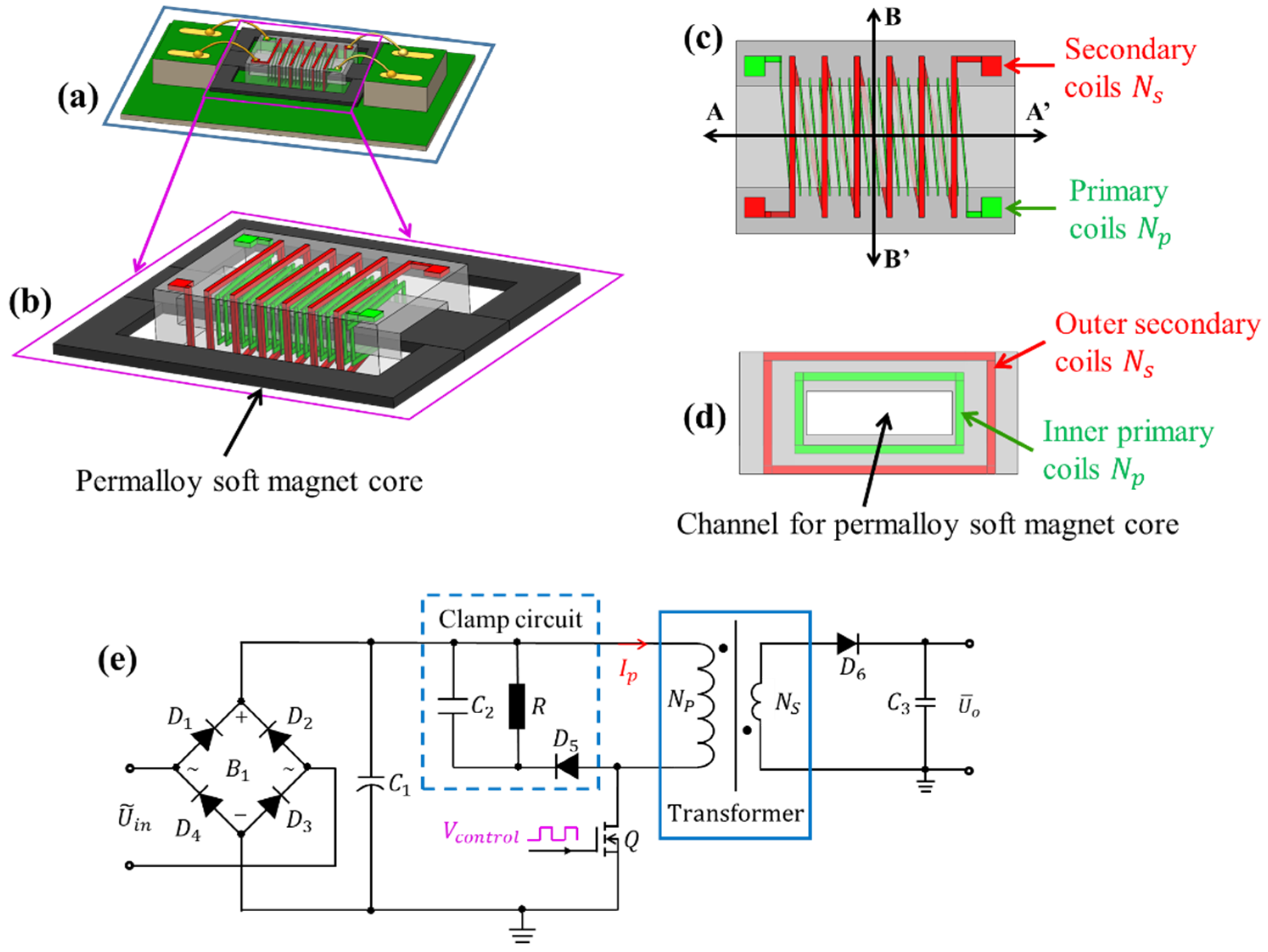
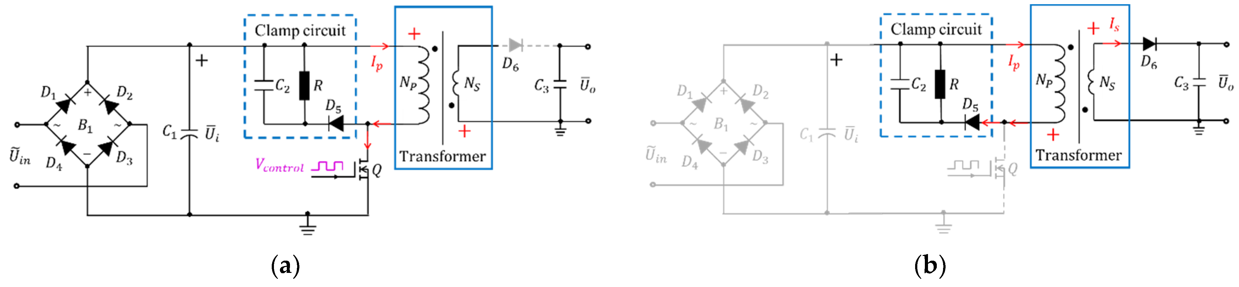
2. Design and Modeling
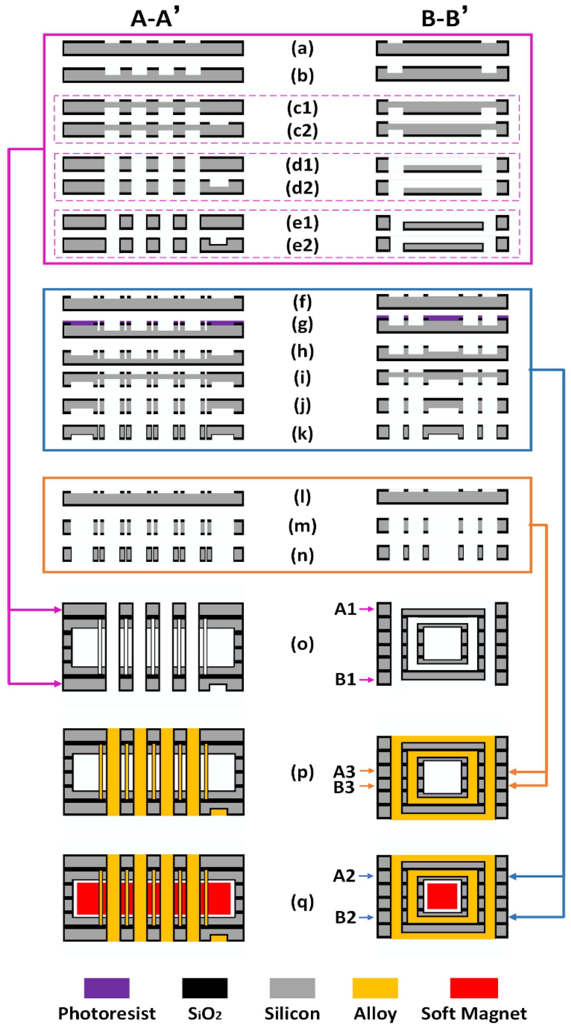
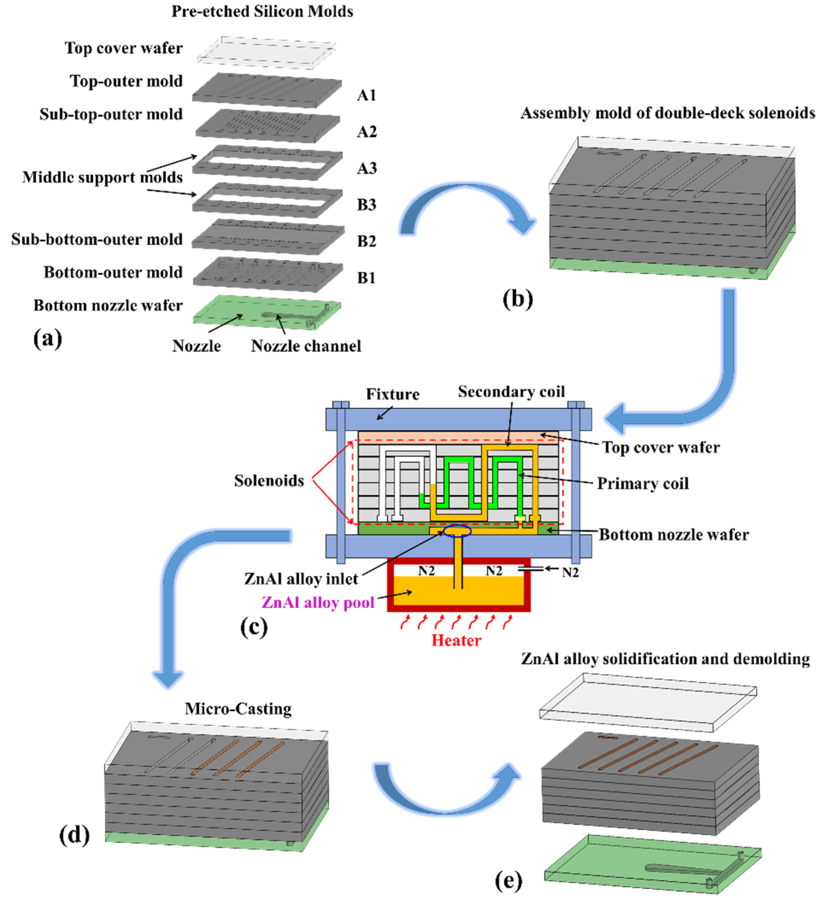
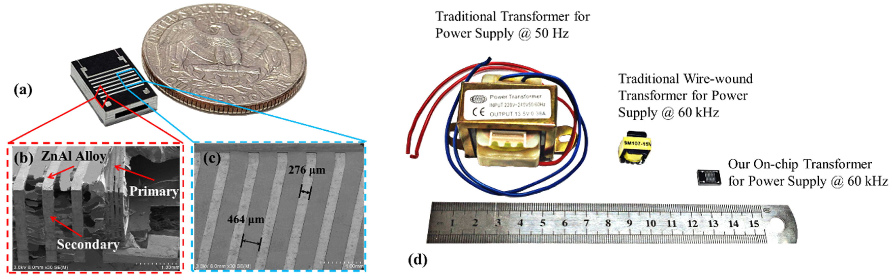
3. Fabrication
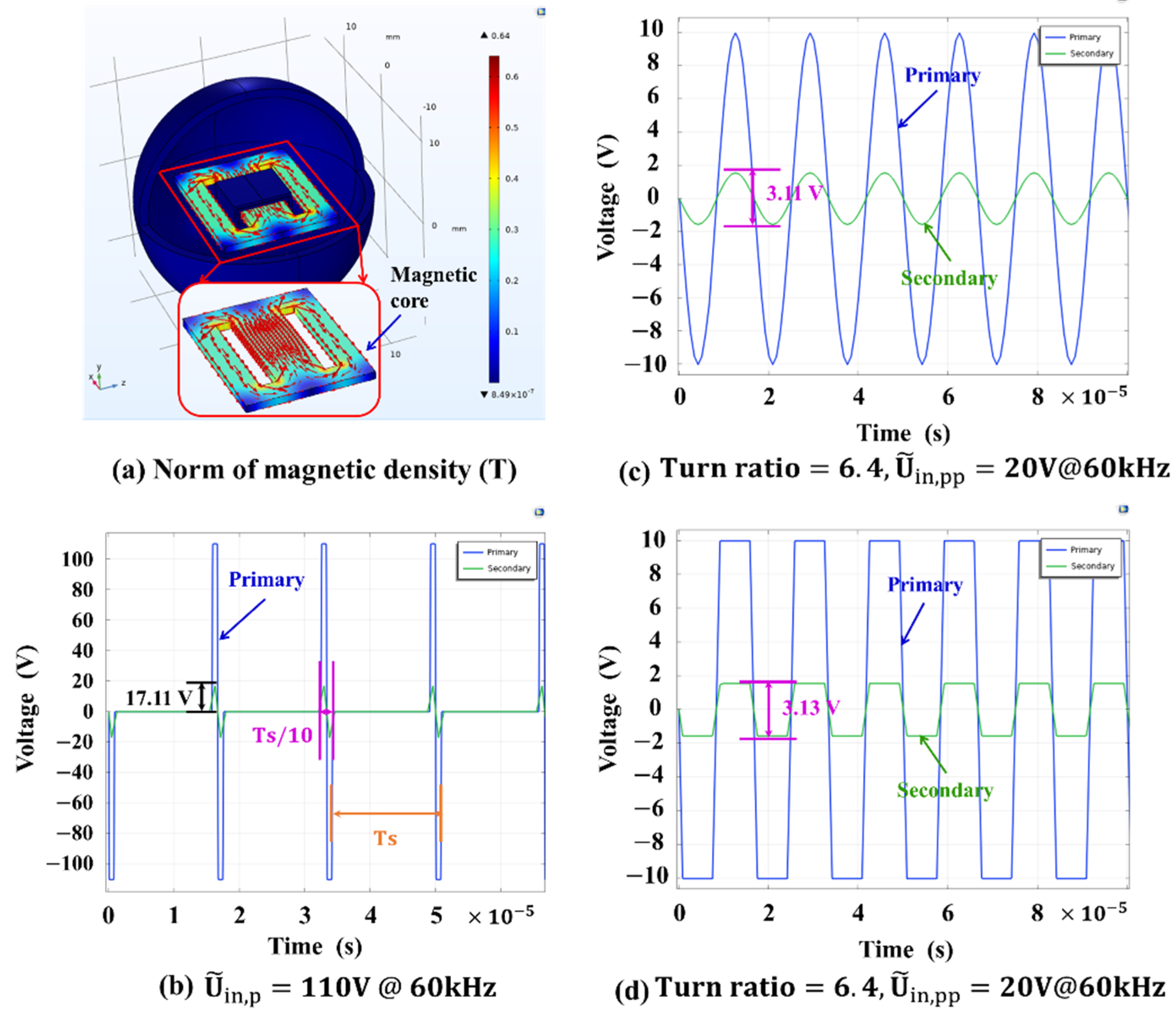
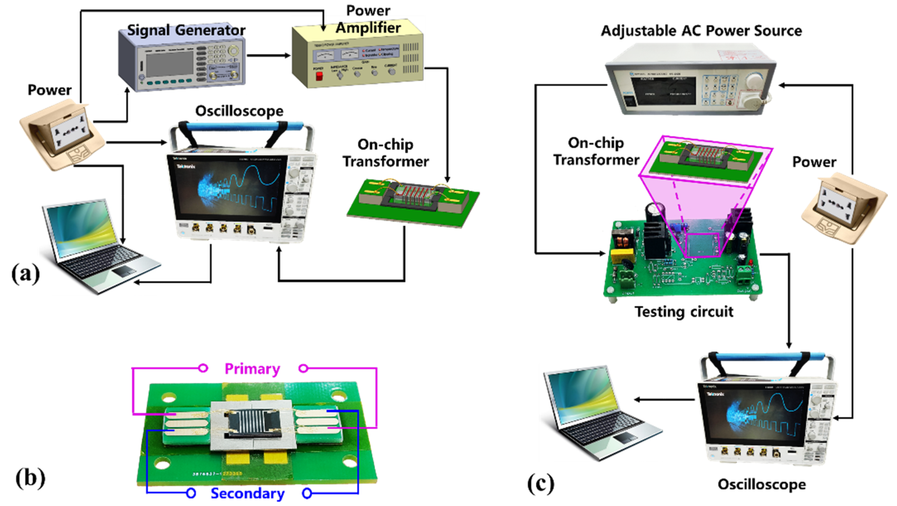
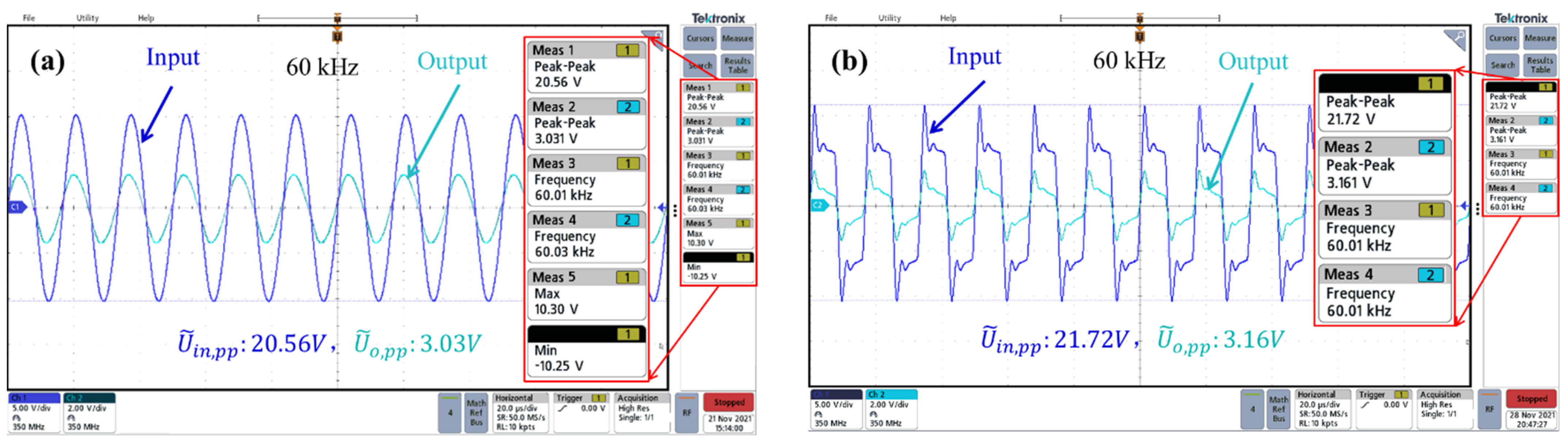
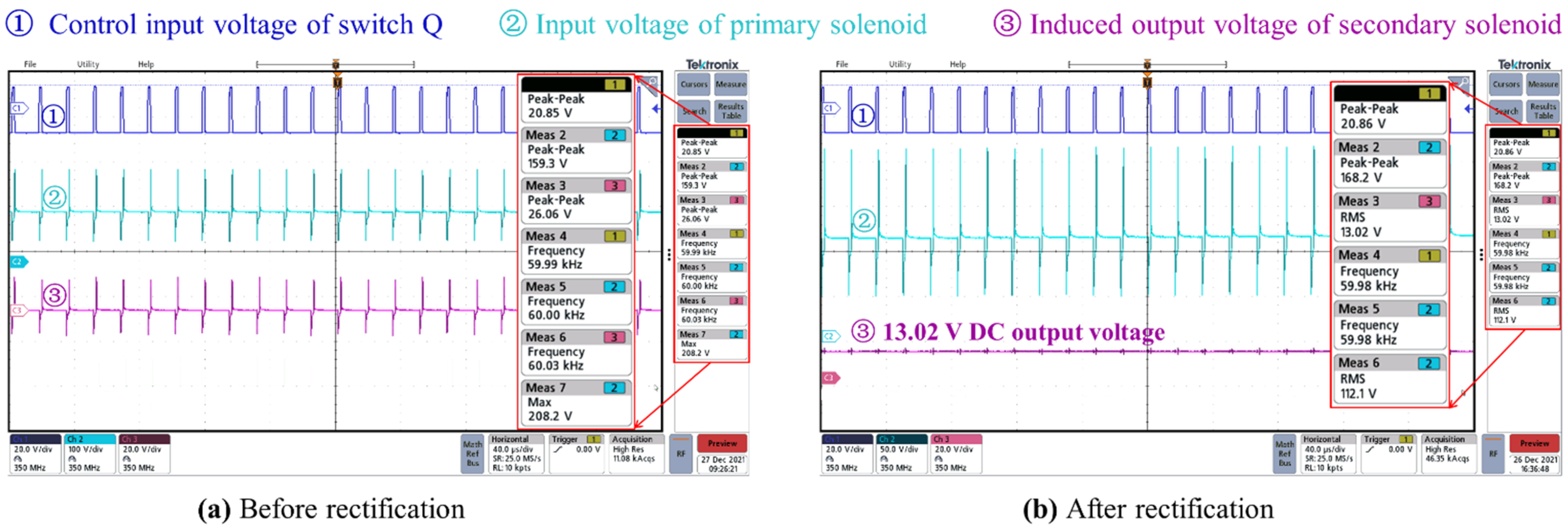
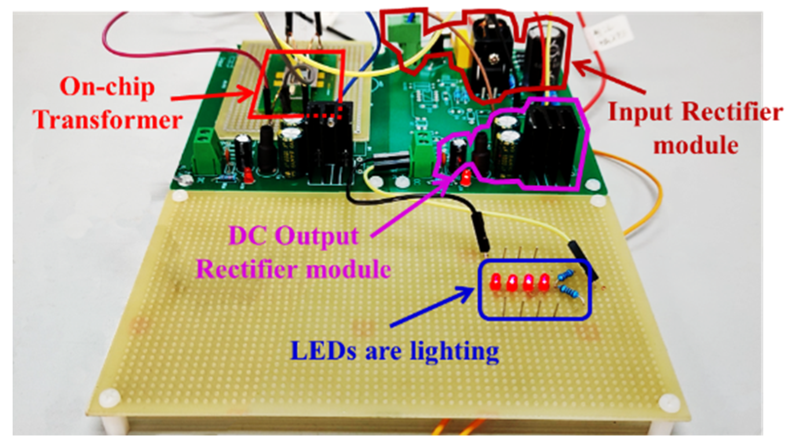
4. Testing Results
5. Conclusions
Author Contributions
Funding
Acknowledgments
Conflicts of Interest
References
- Cheng, C.-A.; Cheng, H.-L.; Chang, C.-H.; Chang, E.-C.; Hung, W.-S.; Lan, L.-F. A novel single-stage high-power-factor LED power supply with soft-switching feature for streetlight applications. In Proceedings of the 2020 International Symposium on Computer, Consumer and Control (IS3C), Taichung City, Taiwan, 13–16 November 2020; pp. 19–21. [Google Scholar]
- Cheng, C.-A.; Chen, Y.-L.; Chen, Y.-J.; Lai, S.-W. A Novel Cost-Effective AC-DC Power Supply for Indoor LED Lighting Applications. In Proceedings of the 2019 IEEE PES Asia-Pacific Power and Energy Engineering Conference (APPEEC), Macao, China, 1–4 December 2019; pp. 1–3. [Google Scholar]
- Lai, W.-C.; Jang, S.-L.; Ciou, Y.-L.; Lee, H.-C.; Su, Y.-J. Low power transformer coupled VCO for wearable sensor applications. In Proceedings of the 2017 6th International Symposium on Next Generation Electronics (ISNE), Keelung, Taiwan, 23–25 May 2017; pp. 1–3. [Google Scholar]
- Fan, X.; Liu, B.; Ding, J.; Deng, Y.; Han, X.; Hu, W.; Zhong, C. Flexible and Wearable Power Sources for Next-Generation Wearable Electronics. Batter. Supercaps 2020, 3, 1262–1274. [Google Scholar] [CrossRef]
- Ho, G.K.; Zhang, C.; Pong, B.M.; Hui, R.S. Bendable transformer for wearable electronics. In Proceedings of the 2015 IEEE Energy Conversion Congress and Exposition (ECCE), Montreal, QC, Canada, 20–24 September 2015; pp. 5865–5871. [Google Scholar]
- Chu, Y.-C.; Chang-Chien, L.-R.; Artan, N.S.; Czarkowski, D.; Chang, C.-H.; Zou, J.; Chao, H.J. On-chip AC–DC multiple-power-supplies module for transcutaneously powered wearable medical devices. IEEE Trans. Ind. Appl. 2017, 54, 1724–1736. [Google Scholar] [CrossRef]
- Hassan, I.; Sayed, K. Design and Analysis of Planar Transformers in Modern Switching Mode Power Supply. Sohag Eng. J. 2021, 1, 32–43. [Google Scholar] [CrossRef]
- Kasireddy, I.; Ch, K.R. An Efficient Selective Harmonic Based Full Bridge DC-DC Converter for LED Lighting Applications. In Proceedings of the 2019 National Power Electronics Conference (NPEC), Tiruchirappalli, India, 13–15 December 2019; pp. 1–6. [Google Scholar]
- Ma, H.; Li, Y.; Chen, Q.; Zhang, L.; Xu, J. A single-stage integrated boost-LLC AC–DC converter with quasi-constant bus voltage for multichannel LED street-lighting applications. IEEE J. Emerg. Sel. Top. Power Electron. 2018, 6, 1143–1153. [Google Scholar] [CrossRef]
- Nigsch, S.; Marquart, J.; Schenk, K. Low cost high density ac-dc converter for led lighting applications. In Proceedings of the PCIM Europe 2016; International Exhibition and Conference for Power Electronics, Intelligent Motion, Renewable Energy and Energy Management, Nuremberg, Germany, 10–12 May 2016; pp. 1–8. [Google Scholar]
- Kim, S.H.; Lee, S.-H. A New High-Performance LED Converter With Separation of the AC and DC Driving Parts for a T8 LED Tube. IEEE Access 2019, 7, 61433–61441. [Google Scholar] [CrossRef]
- Ambatipudi, R.; Kotte, H.B.; Bertilsson, K. High performance planar power transformer with high power density in MHz frequency region for next generation switch mode power supplies. In Proceedings of the 2013 Twenty-Eighth Annual IEEE Applied Power Electronics Conference and Exposition (APEC), Long Beach, CA, USA, 17–21 March 2013; pp. 2139–2143. [Google Scholar]
- Zhang, Z.; He, B.; Hu, D.-D.; Ren, X.; Chen, Q. Multi-winding configuration optimization of multi-output planar transformers in GaN active forward converters for satellite applications. IEEE Trans. Power Electron. 2018, 34, 4465–4479. [Google Scholar] [CrossRef]
- Abdelrahman, A.A.A.; Elfaki, E.E.O.; Salih, A.A.; Adam, H.A.E. Design of High Frequency Transformer for Switch Mode Power Supply. In Proceedings of the 2015 International Conference on Computing, Control, Networking, Electronics and Embedded Systems Engineering (Iccneee), Khartoum, Sudan, 7–9 September 2015; pp. 129–135. [Google Scholar]
- Le, H.T.; Mizushima, I.; Nour, Y.; Tang, P.T.; Knott, A.; Ouyang, Z.W.; Jensen, F.; Han, A.P. Fabrication of 3D air-core MEMS inductors for very-high-frequency power conversions. Microsyst. Nanoeng. 2018, 4, 17082. [Google Scholar] [CrossRef] [Green Version]
- Kumar, R.; Wu, C.-C.; Liu, C.-Y.; Hsiao, Y.-L.; Chieng, W.-H.; Chang, E.-Y. Discontinuous Current Mode Modeling and Zero Current Switching of Flyback Converter. Energies 2021, 14, 5996. [Google Scholar] [CrossRef]
- Pal, S.; Singh, B.; Shrivastava, A. An efficient wide input wide output CrCM flyback converter in high-power LED lighting. Int. Trans. Electr. Energy Syst. 2020, 30, e12445. [Google Scholar] [CrossRef]
- Soma, S.K.; Netapally, R.S.R.; Mallapu, V.K. A Novel Discontinuous Input Current Boost Flyback Converter for LED Applications. In Proceedings of the 2021 2nd International Conference for Emerging Technology (INCET), Belgaum, India, 21–23 May 2021; pp. 1–7. [Google Scholar]
- Myderrizi, I.; Ozbey, E. A low power multiple output switch-mode power supply with wide input range. Analog. Integr. Circuits Signal Processing 2014, 81, 431–441. [Google Scholar] [CrossRef]
- Saket, M.A.; Ordonez, M.; Shafiei, N. Planar transformers with near-zero common-mode noise for flyback and forward converters. IEEE Trans. Power Electron. 2017, 33, 1554–1571. [Google Scholar] [CrossRef]
- Dasohari, M.; Neti, V.; Porpandiselvi, S.; Manikyavani, A.R. An Interleaved Dual Double-Ended Forward Converter Based LED Driver for DC Lighting Grids. In Proceedings of the 2020 21st National Power Systems Conference (NPSC), Gandhinagar, India, 17–19 December 2020; pp. 1–5. [Google Scholar]
- Naik, K.K.; Venugopal, N. Multi Output Forward-Flyback Switch Mode Power Supply. In Proceedings of the 2018 3rd IEEE International Conference on Recent Trends in Electronics, Information & Communication Technology (RTEICT), Bangalore, India, 18–19 May 2018; pp. 1321–1326. [Google Scholar]
- Kim, H.; Cho, Y. Switched Mode Power Supply with High Isolation for High Voltage Applications. In Proceedings of the 2020 IEEE PELS Workshop on Emerging Technologies: Wireless Power Transfer (WoW), Seoul, Korea, 15–19 November 2020; pp. 201–205. [Google Scholar]
- Eguchi, K.; Kuwahara, K.; Ishibashi, T. Analysis of an LED lighting circuit using a hybrid buck–boost converter with high gain. Energy Rep. 2020, 6, 250–256. [Google Scholar] [CrossRef]
- Piazza, G.L.; Alves, R.L.; Font, C.H.I.; Barbi, I. Resonant circuit model and design for a high frequency high voltage switched-mode power supply. In Proceedings of the 2009 Brazilian Power Electronics Conference, Bonito-Mato Grosso do Sul, Brazil, 27 September–1 October 2009; pp. 326–331. [Google Scholar]
- Ou, S.-Y.; Hsiao, H.-P. Analysis and design of a novel single-stage switching power supply with half-bridge topology. IEEE Trans. Power Electron. 2011, 26, 3230–3241. [Google Scholar] [CrossRef]
- Gu, J.; Liu, B.; Chen, G.; Li, X. Study of a through-silicon/substrate via filling method based on the combinative effect of capillary action and liquid bridge rupture. J. Micromech. Microeng. 2016, 26, 075009. [Google Scholar] [CrossRef]
- Gu, J.; Guo, Z.; Yang, H.; Li, X. A micro-casting method for solenoid coil fabrication. In Proceedings of the 2017 19th International Conference on Solid-State Sensors, Actuators and Microsystems (TRANSDUCERS), Toronto, ON, Canada, 17–20 June 2019; pp. 1108–1111. [Google Scholar]
- Tong, Z.; Braun, W.D.; Rivas-Davila, J.M. 3-D printed air-core toroidal transformer for high-frequency power conversion. In Proceedings of the 2019 20th Workshop on Control and Modeling for Power Electronics (COMPEL), Kaohsiung, Taiwan, 18–22 June 2017; pp. 1–7. [Google Scholar]
- Xu, T.; Sun, J.; Wu, H.; Li, H.; Li, H.; Tao, Z. 3D MEMS In-Chip Solenoid Inductor with High Inductance Density for Power MEMS Device. IEEE Electron Device Lett. 2019, 40, 1816–1819. [Google Scholar] [CrossRef]
- Yu, X.; Kim, M.; Herrault, F.; Ji, C.-H.; Kim, J.; Allen, M.G. Silicon-embedding approaches to 3-D toroidal inductor fabrication. J. Microelectromech. Syst. 2013, 22, 580–588. [Google Scholar] [CrossRef]


| Symbol | Value |
|---|---|
| The input AC voltage at 50 Hz or 60 Hz | |
| DC input voltage after is rectified by Rectifier bridge | |
| DC output voltage after rectification | |
| Current flowing through the primary solenoid | |
| Current flowing through the secondary solenoid | |
| Rectifier bridge for the input AC voltage | |
| Diode 1 for rectifier bridge | |
| Diode 2 for rectifier bridge | |
| Diode 3 for rectifier bridge | |
| Diode 4 for rectifier bridge | |
| Diode 5 for clamp circuit | |
| Diode 6 for DC output rectification | |
| Capacitor 1 for input voltage filtering | |
| Capacitor 2 for clamp circuit | |
| Capacitor 3 for output voltage filtering | |
| Resistance for clamp circuit | |
| Primary solenoid of the transformer | |
| Secondary solenoid of the transformer | |
| Switch transistor |
| Parameter | Symbol | Value |
|---|---|---|
| Turns of primary solenoid coils | 45 | |
| Width of primary coil | 86 | |
| Depth of primary coil | 290 | |
| Turns of secondary solenoid coils | 7 | |
| Width of secondary coil | 276 | |
| Depth of secondary coil | 290 | |
| Inductance of the primary solenoid with air core | 3.01 | |
| Inductance of the secondary solenoid with air core | 0.13 | |
| Width of the channel for magnetic core | 5 | |
| Height of the channel for magnetic core | 0.92 | |
| Length of the transformer chip | 8.5 | |
| Width of the transformer chip | 6.6 | |
| Thickness of the transformer chip | 2.5 | |
| Switching frequency of switch Q | 60 | |
| Input AC voltage | 110 | |
| Frequency of input AC voltage | 50 or 60 |
| Reference | Structure Type of Transformer Coils | In-Substrate or On-Substrate | Number of Turns (Np:Ns) | Working Frequency | Volume (cm3) | Inductance Density of Primary Coils (μH/cm3) | Inductance Density of Secondary Coils (μH/cm3) |
| This work | Solenoid | In-substrate | 45:7 | 60 kHz | 0.689 | 54.3 | 1.6 |
| [29] | 3D-printedtoroid | On-substrate | 19:12 | 40.68 MHz | 14.2 | 0.02 | 0.007 |
| [15] | Toroid | Concave-suspending in substrate | 25 | 30–72 MHz | 0.3 mm3 | 13.6–17.3 | - |
| [30] | Solenoid | In-substrate | 20 | 21 MHz | 4 mm3 | 18.3–21.7 | - |
| [28] | Solenoid | In-substrate | 20 | >1 MHz | 1.496 mm3 | 10.2 | - |
| [31] | Toroid | Concave-suspending in substrate | 25 | 40–10 MHz | 29.7 mm3 | 1.16–2.02 | - |
Publisher’s Note: MDPI stays neutral with regard to jurisdictional claims in published maps and institutional affiliations. |
© 2022 by the authors. Licensee MDPI, Basel, Switzerland. This article is an open access article distributed under the terms and conditions of the Creative Commons Attribution (CC BY) license (https://creativecommons.org/licenses/by/4.0/).
Share and Cite
Wang, N.; Chen, C.; Chen, P.; Gu, J.; Pan, P.; Han, R.; Liu, M.; Li, X. MEMS-Casting Fabricated Chip-Style 3D Metal Solenoidal Transformers towards Integrated Power Supply. Micromachines 2022, 13, 325. https://doi.org/10.3390/mi13020325
Wang N, Chen C, Chen P, Gu J, Pan P, Han R, Liu M, Li X. MEMS-Casting Fabricated Chip-Style 3D Metal Solenoidal Transformers towards Integrated Power Supply. Micromachines. 2022; 13(2):325. https://doi.org/10.3390/mi13020325
Chicago/Turabian StyleWang, Nianying, Changnan Chen, Pu Chen, Jiebin Gu, Pichao Pan, Ruofeng Han, Min Liu, and Xinxin Li. 2022. "MEMS-Casting Fabricated Chip-Style 3D Metal Solenoidal Transformers towards Integrated Power Supply" Micromachines 13, no. 2: 325. https://doi.org/10.3390/mi13020325