Article

Dynamic Enhancement for Dual Active Bridge Converter with a Deadbeat Current Controller

1
Unit 91977 of the Chinese People’s Liberation Army, Beijing 100036, China
2
School of Automotive Engineering, Wuhan University of Technology, Wuhan 430070, China
*
Author to whom correspondence should be addressed.
Micromachines 2022, 13(12), 2048; https://doi.org/10.3390/mi13122048
Submission received: 21 October 2022 / Revised: 13 November 2022 / Accepted: 18 November 2022 / Published: 23 November 2022
(This article belongs to the Special Issue Advanced Interconnect and Packaging)

Abstract

:
This paper investigates the deadbeat current controllers for isolated bidirectional dual-active-bridge dc-dc converter (IBDC), including the peak current mode (PCM) and middle current mode (MCM). The controller uses an enhanced single phase shift (ESPS) modulation method by exploiting pulse width as an extra control variable in addition to phase shift ratio. The control variables for PCM controllers are derived in detail and the two different current controllers are compared. A double-closed-loop control method is then employed, which could directly control the high-frequency inductor current and eliminate the transient DC current bias of the transformer. Furthermore, load feedforward was introduced to further enhance the dynamic of the converter. With the proposed control method, the settling time could be reduced within several PWM cycles during load disturbance without transient DC current bias. A 5 kW IBDC converter prototype was built and the settling time of 6 PWM cycles during load change with voltage regulation mode was achieved, which verifies the superior dynamic performance of the control method.

1. Introduction

The isolated bi-directional dual-active-bridge dc-dc converter (IBDC) has been a hot topic in recent years due to its simple structure, high efficiency and ultrafast response [1]. The transient DC current offset of the transformer and the inductor, which might saturate the transformer and increase the system’s current stress during the abrupt load change, has attracted people’s attention. Different dynamic modulation methods have been proposed to solve the problem [2,3,4,5]. Additionally, to increase the dynamics of IBDCs, the current mode controller could be a competitive alternative. It also has other inherent benefits including over-current protection, elimination of transient DC current offset and easy implementation of current sharing between multiple IBDCs [6].
Digital predictive current controllers based on conventional single phase shift (CSPS) modulation was proposed in [7,8], where the phase shift ratio was used to control the transformer current. In [7], the average current calculated by an analog integrator of the DC bus current was used as the feedback signal, which can achieve fast dynamic performance. However, transient DC current offset occurs during the sudden change in phase shift ratio for CSPS modulation.
The predictive duty cycle mode (PDCM) controller, shown in Figure 1b, was proposed in [6] to eliminate the transient DC current offset, which was applied in [8]. The drive signals of the primary side are fixed. The transformer current needs to be oversampled, and duty cycles d1 for S2,3 and d2 for S1,4 are calculated in turn in every half cycle. Another limitation of this method is that the controller only works in the ZVS range (IP1 > 0) shown in Figure 1b and may lose effectiveness when IP1 < 0.
A deadbeat current controller based on the middle current and enhanced PWM modulation was proposed in [9]. However, regulation of the output voltage and current was not introduced, which is more important in real application. To overcome the drawbacks, this paper investigated the deadbeat current controllers, including the peak current mode (PCM) and middle current mode (MCM). Based on the controllers, a double-closed-loop control method with load feedforward was introduced. Furthermore, a 5 kW IBDC converter prototype was built, and the settling time of 6 PWM cycles during load change could be achieved, which validates its superior dynamic performance.

2. Deadbeat Peak Current Mode Controller

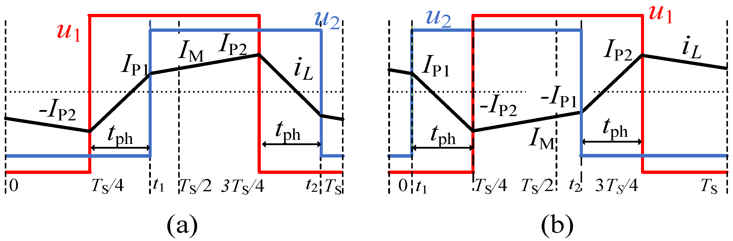
2.1. Basic Model of IBDC for SPS Modulation

The basic model of SPS modulation-based IBDC is presented prior to introducing the proposed current controller. Figure 2 illustrates the theoretical waveforms of the IBDC using the SPS modulation method when converter voltage gain k 1 , where k = V1/(nV2) and n is the turn ratio of the transformer. The waveforms are symmetrical for the same transmission power of two opposite directions.
The symbols in Figure 2 are defined as follows: TS is the switching cycle, f is the switching frequency, D is the phase shift ratio and tph is the shifted time. D ≥ 0 (tph ≥ 0) stands for P ≥ 0 and D < 0 (tph < 0) for P < 0. IP1 and IP2 are the two “switching currents” and IP2 is the peak current when k > 1. The middle current IM, defined as the instantaneous current at TS/2, is taken into consideration instead of the average current, which equals zero in one cycle. The basic equations for the IBDC are derived as follows:
{ P = V 1 2 2 f L k D ( 1 | D | )   ,   t ph = D T S 2 I P 1 = V 1 ( 2 k | D | k + 1 ) 4 f L k ,   I P 2 = V 1 ( 2 | D | + k 1 ) 4 f L k ,   I M = V 1 D 2 f L k
The relationships among the variables P, IP1, IP2, IM, D and tph at steady state can then be derived. Therefore, for a given value of one variable, other variables can be calculated.

2.2. Peak Current Mode Controller

Peak current mode (PCM) controllers are introduced in this section. Figure 3a,b show the transient waveforms of a PCM current controller in one cycle for forward and reverse power transmission, respectively. P1, P2, P3 and P4 are the drive signals for the primary side and S1, S2, S3 and S4 are the drive signals for the secondary side. The variable tph,ref is shifted-time at the steady state for the given IP2,ref which can be derived from (1). A sawtooth carrier with the same frequency of the converter was utilized to generate the reference signals. The “switching on” moment t1 and “switching off” moment t2 should meet the constrains as: 0 < t1 < TS/2 and 3TS/4 < t2 < TS. The variables tD and tW are defined as “delay time” and “width time”, respectively. Pref is the power reference, and IP2,ref and IP1,ref are the references for the corresponding “switching currents”, respectively.
As shown in Figure 3a, there are two cases according to the initial current I0 and reference current Ip2,ref: u2 leads u1 (tph < 0) for the solid line waveforms and u2 lags u1 (tph > 0) for dotted line waveforms. For the sake of brevity, the superposition principle was used to derivate the inductor current when calculating tD and tW.
For forward power transmission, the requirement was imposed that IP2 = IP2,ref and tph,ref > 0. According to the superposition principle, the inductor current ripple Δ I L during 0 and 3TS/4 can be calculated by adding up the two ripple currents as follows:
{ Δ I L = Δ I L , u 1 + Δ I L , u 2   Δ I L , u 1 = V 1 L T S 4 + V 1 L T S 2   ,   Δ I L , u 2 = V 2 L t D + V 2 L ( 3 T S 4 t D ) I P 2 = I 0 + Δ I L = I P 2 , ref
where Δ I L , u 1 and Δ I L , u 2 are current ripples generated by the two dependent voltage source u1 and u2, respectively. tD is then derived as:
t D = ( I P 2 , ref I 0 ) L k 2 V 1 + 3 k 8 f
Furthermore, tW is derived as:
t W = 3 T S 4 t D + t ph , ref
With regard to reverse power transmission, the switching current at t2 is set to be—IP1,ref and tph,ref < 0 as shown in Figure 4. Similar to forward power transmission, tD and tW can be obtained. Thus, the equations for the PCM controller are written as:
{ t D = k L ( I P 2 , ref I 0 ) 2 V 1 + 3 k 8 f ;   t W = k L ( I P 2 , ref + I 0 ) 2 V 1 k 5 8 f ,   P ref 0 t D = k L ( I P 2 , ref + I 0 ) 2 V 1 + k + 1 8 f ;   t W = k L ( I P 2 , ref I 0 ) 2 V 1 + k + 3 8 f ,   P ref < 0
As in the aforementioned Equations (6) and (7), initial current I0 is sampled to calculate the tD and tW. However, a one-cycle delay exists between the sampling instant and control update due to the algorithm implementation of the digital processor. IP2 for the PCM controller is sampled at 3TS/4, and DSP interrupt occurs to calculate the new parameters shown in Figure 3. tD and tW update at the beginning of the next cycle. Assuming DC bus voltage V1 and V2 are constant in two adjacent periods, the relationships between the IP2(n − 1), IM(n − 1) in the (n − 1)th cycle and the initial current in the nth switching cycle I0(n) could be derived as:
I 0 ( n ) = { I P 2 ( n 1 ) 2 V 1 ( k - 1 ) L k ( t D ( n 1 ) + t W ( n 1 ) ) + V 1 ( 7 - k ) 4 f L k   ,   P ref ( n 1 ) 0 I P 2 ( n 1 ) V 1 ( k - 1 ) 4 f L k ,   P ref ( n 1 ) < 0
According to the power transmission directions in two adjacent cycles, four situations are considered for the PCM controller: case 1 when Pref(n − 1) 0 and Pref(n) 0; case 2 when Pref(n − 1) < 0 and Pref(n) 0; case 3 when Pref(n − 1) 0 and Pref(n) < 0; and case 4 when Pref(n − 1) < 0 and Pref(n) < 0. Combining (6)–(9), the control variables tD and tW with delay compensation can be derived as shown in Table 1. With the control variables in Table 1, the inductor peak current could be tracked to the reference in two cycles, which is consistent with the idea of the deadbeat control in ref [10].

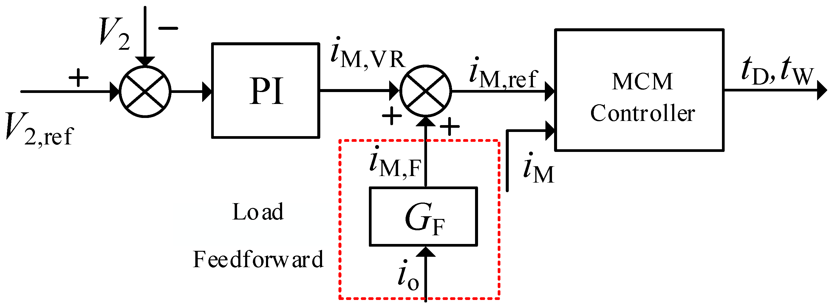
3. Double-Closed-Loop Control with Load Feedforward

In practice, instead of the high-frequency inductor current, the DC voltage, current or power should always be regulated. In this section, the voltage mode control strategy based on the MCM-ESPS controller is introduced.
Figure 4 shows the output voltage control scheme based on the deadbeat current controller, where two control loops are involved. The load feedforward control could substantially increase the system dynamic [11,12]. In order to improve the stability of output voltage under load disturbance, load feedforward under double-closed-loop control is presented. As shown in Figure 4, the feedforward current iM,F corresponding to the load was superimposed on the current reference iM,VR, which is the output of the outer voltage loop, to form the final current reference value iM,ref.
The relationships of the middle current were derived as:
I M = { V 1 2 f L k ( 1 2 1 4 2 f L k P V 1 2 )   ,   P 0 V 1 2 f L k ( 1 2 1 4 + 2 f L k P V 1 2 )   ,   P < 0
Without considering the power loss of the converter, we could obtain:
P = V 2 i o
Thus, the relationship between the middle current IM and the load current io could be expressed as (9) and (10):
I M = { V 1 2 f L k ( 1 2 1 4 2 f L i o V 1 )   ,   i o 0 V 1 2 f L k ( 1 2 1 4 + 2 f L i o V 1 )   ,   i o < 0
i o = N I M ( 1 2 f L k I M V 1 )
The small signal model of the system, as shown in Figure 5, can be obtained from the control block diagram in Figure 4, where iS is the average output current of an H bridge in a single period and Go(s) is the transfer function of capacitance voltage and capacitance current, denoted as:
G o ( s ) = 1 / ( C 2 s )
GVR(s) is the volatge regulation transfer function, where the conventional PI controller is always used. KP and KI are the proportional and integral coefficients of the PI regulator, respectively. Thus, we could obtain:
G VR ( s ) = K P + K I s
GF(s) represents the transfer function of the load feedforward and GMS(s) is the relationship between iM and is. GC(s) is the transfer function of the deadbeat current controller. Considering a one-cylce delay, it could be written as:
G C ( s ) = 1 e s T s s
The feedforward transfer function GF(s) can be calculated using small-signal analysis based on Equation (10). To substitute i o = i ¯ o + i o and I M = I ¯ M + I M into (10), ignoring the higher-order terms, GF(s) be derived as:
G F ( s ) = I M , F ( s ) / i o ( s ) = 1 / ( N ( 1 4 f L k I M / V 1 ) )
The average output current of H bridge in the secondary side is derived as:
i s = V 1 N 2 f L D ( 1 D )
Combing (1) with (16), the GMS(s) could be derived as:
G MS ( s ) = i S ( s ) / I M ( s ) = N ( 1 4 f L k I M / V 1 )
According to the small signal model in Figure 5, the output impedance Ro1(s) without and with feedforward could be calculated as (17) and (18), respectively.
R o 1 ( s ) = V 2 ( s ) i o ( s ) = G o ( s ) 1 + G VR ( s ) G C ( s ) G MS ( s ) G o ( s )
R o 2 ( s ) = V 2 ( s ) i o ( s ) = ( G F ( s ) G C ( s ) G MS ( s ) - 1 ) G o ( s ) 1 + G VR ( s ) G C ( s ) G MS ( s ) G o ( s )
By substituting the circuit parameters and control parameters into Equations (17) and (18), baud diagrams of output impedance with different loads under the double-closed-loop control strategy can be drawn as shown in Figure 6. In this case, the inductance L = μH, the voltage V1 = 300V and V2 = 280V.The coefficients of the PI regulator are KP = 2 and KI = 4000.
As shown in Figure 6, the closed-loop output impedance at low frequency decreases significantly after the feedforward is added. When IM = 4 A, the output impedance at a frequency of 100 Hz decreases from −15 dB to −35 dB, whereas when IM = 15 A, the output impedance decreases from −8 dB to −30 dB at 100 Hz. If the frequency is further reduced, the amplitude attenuation of the closed-loop output impedance brought by the feedforward control become more obvious, which indicates a more robust output voltage under the load disturbance.

4. Experimental Verification

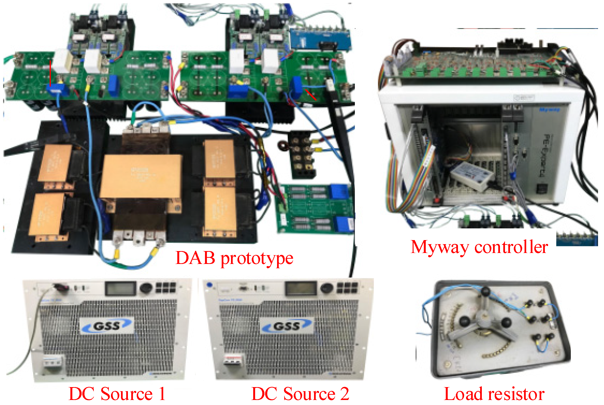
4.1. Experimental Platform

The laboratory IBDC experimental platform shown in Figure 7 was used to verify the proposed control method. The main circuit parameters are listed in Table 2. The current sensor LA55-P had a 200 kHz bandwidth from LEM. PE-Expert4 from Myway was utilized as the digital controller including DSP and FPGA cores. FPGA XC6SLX45 was used to generate PWM signals. The control variables were calculated in each cycle in DSP, and the corresponding PWM compare values CMP1 and CMP2 were updated at the beginning of the next cycle.

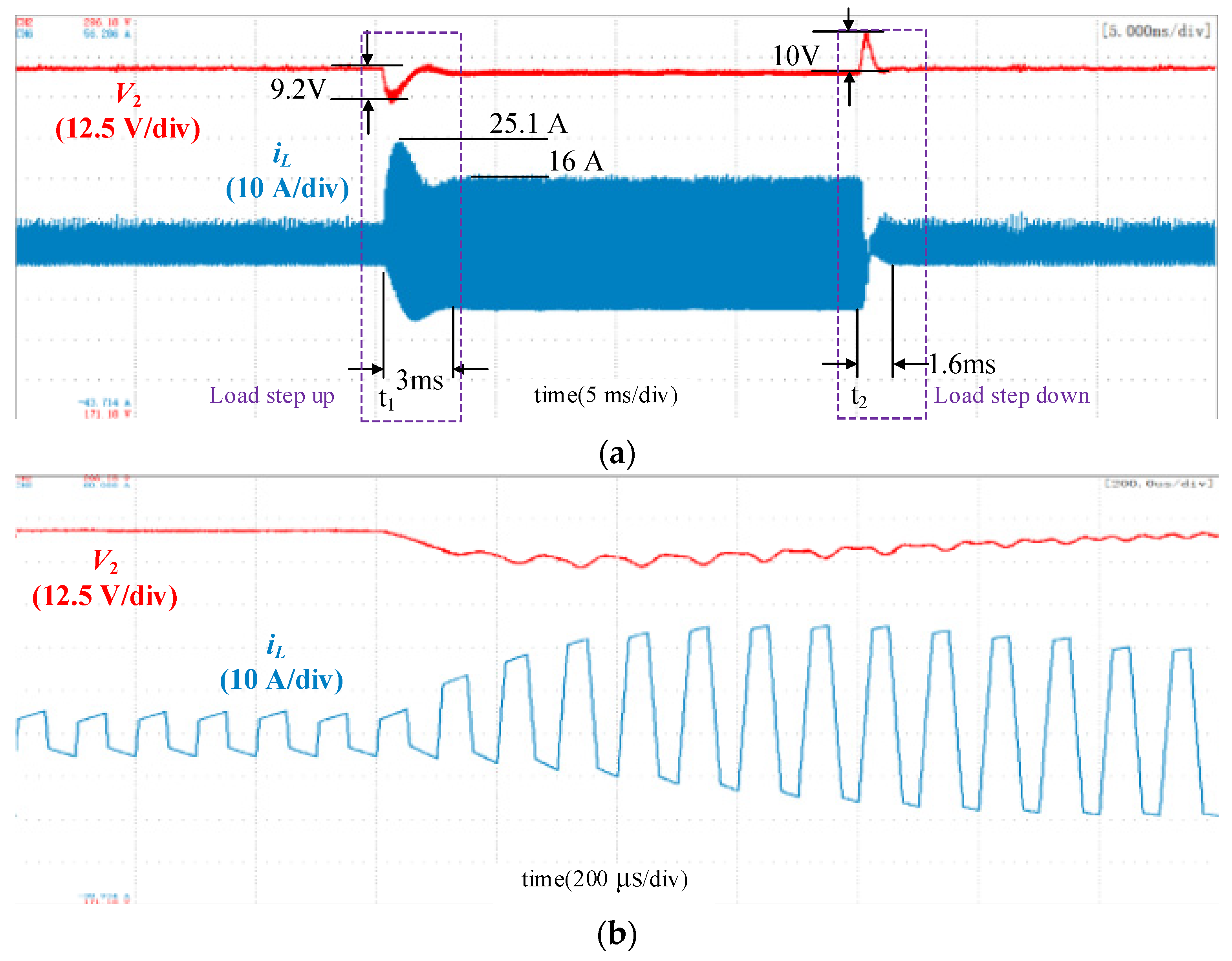
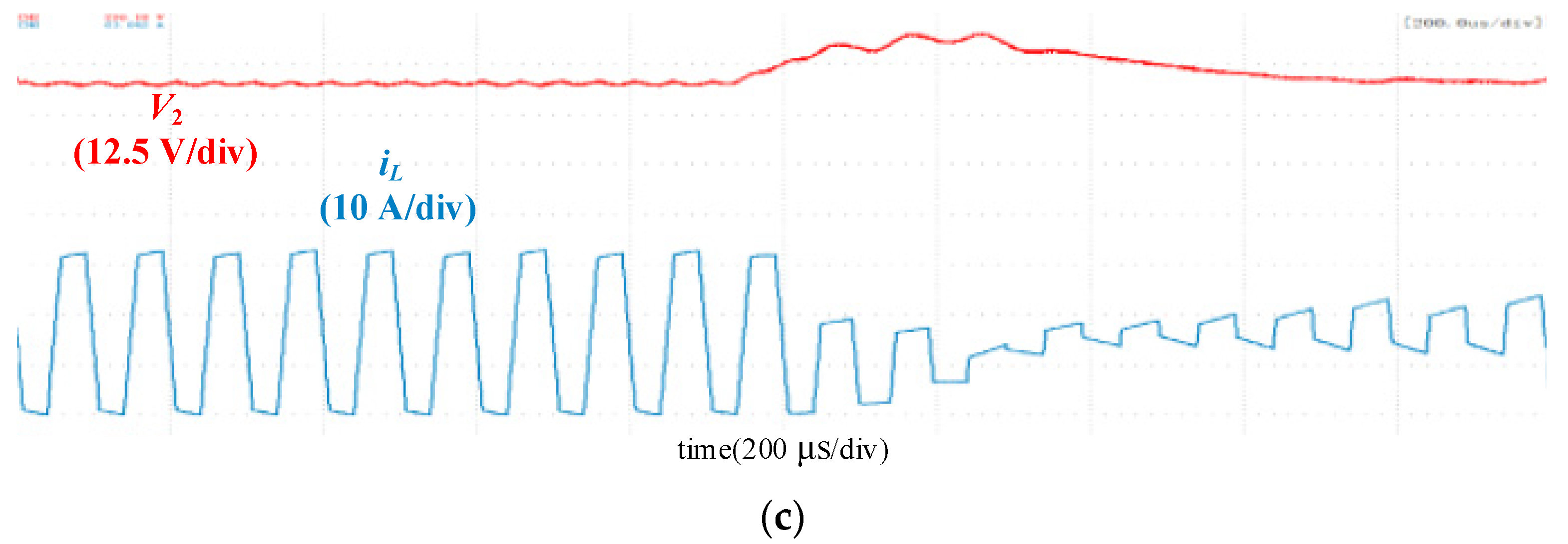
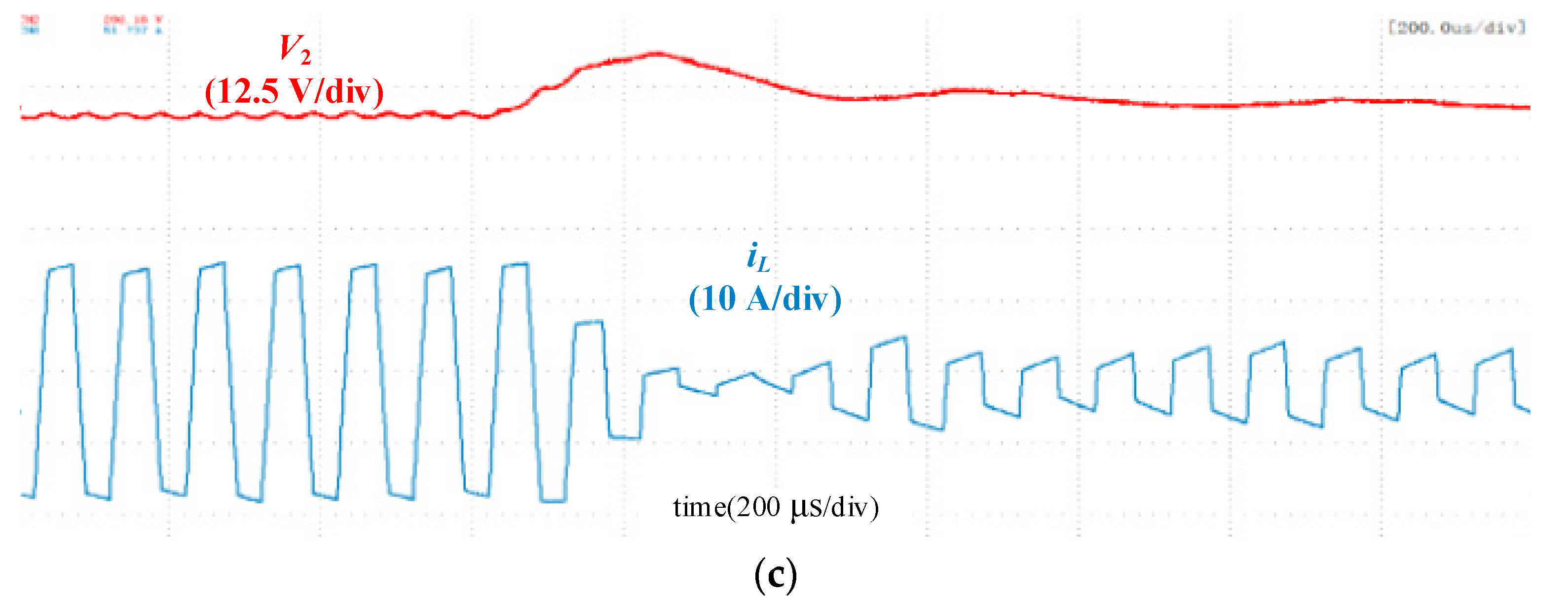
4.2. Comparisons of Different Current Controllers for Forward Power Transmission

The performance of the CSPS modulation-based current controller in [5] and the proposed ESPS-PCM were compared for the forward power transmission mode.
Figure 8 shows the experimental waveforms of current iL when the references have step changes. The references could be tracked for all the controllers when the current reference steps up from 3 A to 8 A and steps down from 8 A to 3 A. The settling time tset in Figure 8a is obvious, while the settling time in Figure 8b is negligible. Additionally, the ESPS-PCM controller eliminates the transient DC current offset that exists in CSPS modulation-based controller, as shown in the dashed circle of Figure 8a.
To verify the performance of the current controllers during bidirectional power transmission, a sequence of current references was set to investigate the response. Figure 9 shows the waveforms of the ESPS-PCM controller. The transmission power P stepped up from 600 W to 1450 W at t1, changed direction to −1450 W at t3, reversed direction to 1450 W at t5 and then stepped down to 600 W at t7. The current references were smoothly reached with a one-cycle delay during the whole transient process, including the transition between two opposite power transmissions.

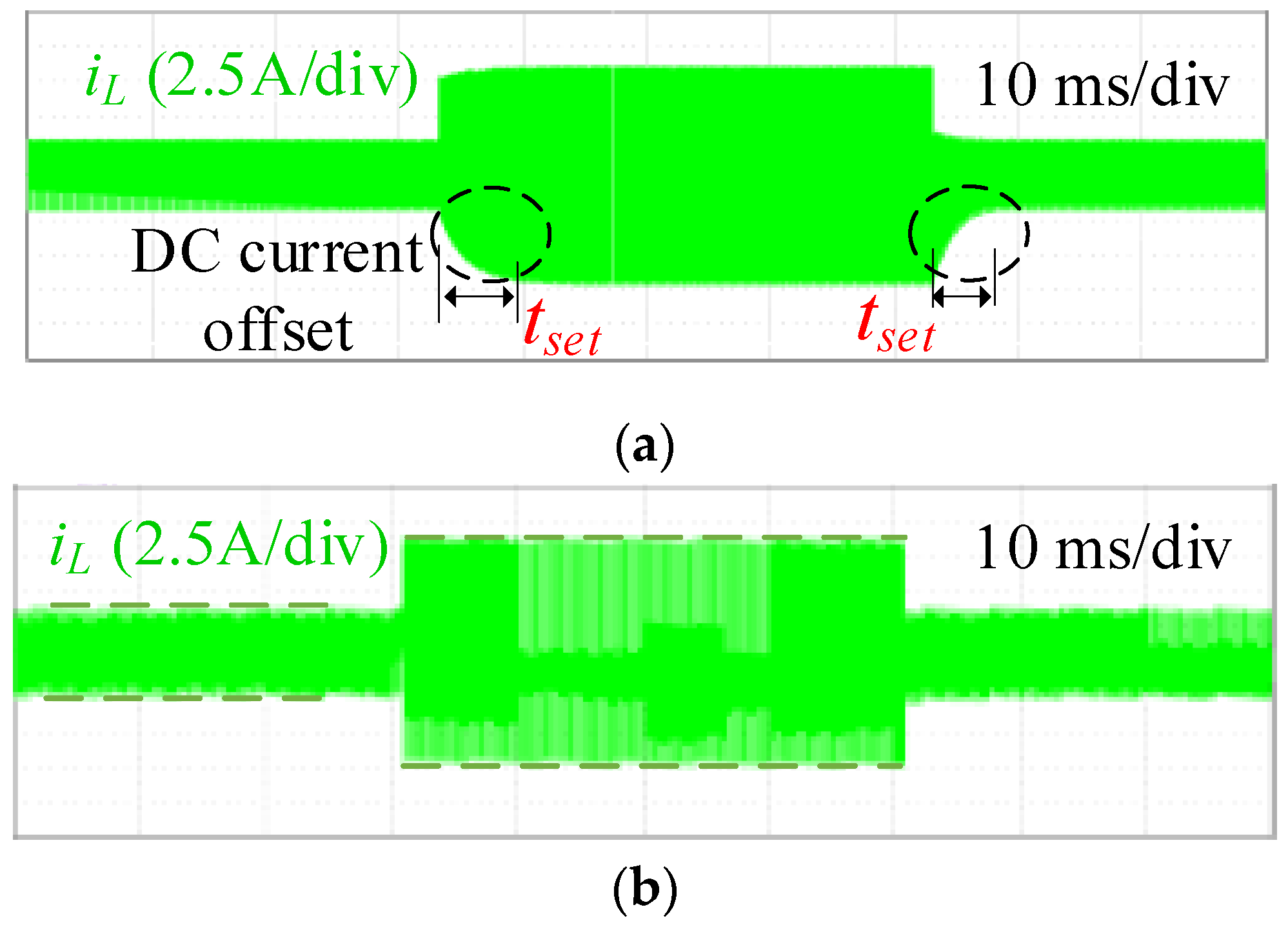
4.3. Dynamic Performance Comparison between Different Control Methods

The experimetal results with traditional single-voltage loop control, double-closed-loop control and double-closed-loop control with feedforward under load disturbance are shown in Figure 10, Figure 11 and Figure 12. The output voltage V2 was 280 V, and the load increased abruptly at t1 with load resistance decreases from 75 Ω to 25 Ω and decreased sharply at t2 with load resistance increases from 25 Ω to 75 Ω. When the load increases, the DC voltage will fall, and the control loop will increase the phase shift angle to transfer more power to maintain the DC load. Simillarly, when the DC load decreases, the DC voltage will rise and the control loop will decrease the phase shift angle to reduce the transmitted power.
Figure 10 shows the waveform using the conventional single-loop control. The inductor current shows obvious transient DC bias during abrupt load change. When the load increased, the peak current reached 25.1 A, and the current overshoot was 9.1 A. In the experiment, both the static and dynamic performances under load increase and decrease were considered when tuning the PI parameters. The waveform showed that the voltage sag was 9.2 V, and the settling time was 3 ms when the load increased. The voltage overshoot was 10 V, and the settling time was 1.6 ms when the load decreased. Figure 11 shows the waveform using the double-closed-loop control. The inductor current was symmetrical, and the transient DC bias was eliminated. When the load increased, the voltage sag was 8.2 V, and the settling time was 1.9 ms. The voltage overshoot was 9 V, and the settling time was 1.3 ms when the load decreased.
Figure 12 shows the waveforms using the double-closed-loop control with load feedforward. The transient DC bias was eliminated. During the transient process, the DC voltage variation was significantly reduced, and the settling time was obviously shortened compared with the double-closed-loop control without load feedforward. The voltage sag was 3 V when the load increased, and the voltage overshoot was 4.4 V when the load decreased. In the process of load surge, the recovery time for DC voltage was 0.5 ms, which is five switching cycles. The recovery time was 0.6 ms, which is six switching cycles, in the process of load decreases.
Compared with the traditional single-voltage loop control, the double-closed-loop control utilizes the deadbeat current controller as the inner loop, which directly regulates the high-frequency AC current of the transformer. Thus, the transient DC current bias could be eliminated. Meanwhile, the dynamic performance the of the IBDC with voltage mode mainly depends on the bandwidth of the feedback signal [12]. With the feedforward control samples, the load changes directly, which could significantly increase the robutness of the DC voltage under the load disturblances. The dynamic performance enhancement of the proposed control can be seen by comparison of Figure 11 and Figure 12.

5. Conclusions

A double-closed-loop control strategy based on the deadbeat current controller was proposed in this paper, which directly regulates the high-frequency inductor current to the reference and eliminates the transient DC current bias during the transient process. Furthermore, load feedforward was introduced to enhance the dynamic of the converter. The proposed control method shows potential in the application of IBDC under voltage mode. With the proposed method, the settling time could be reduced to within several PWM cycles during load disturbance. A 5 kW IBDC converter prototype was built, and the superior dynamic performance of the proposed control strategy was verified by the experimental results.

Author Contributions

Conceptualization, C.T. and S.W.; methodology, S.W.; software, S.W.; validation, S.W.; formal analysis, J.X. and T.B.; investigation, C.T.; resources, S.W.; data curation, J.X.; writing—original draft preparation, T.B.; writing—review and editing, S.W. and J.X.; visualization, C.T.; supervision, C.T.; project administration, C.T.; funding acquisition, C.T. All authors have read and agreed to the published version of the manuscript.

Funding

This research received no external funding.

Data Availability Statement

Not applicable.

Conflicts of Interest

The authors declare no conflict of interest.

References

  1. Hou, N.; Li, Y. Overview and comparison of modulation and control strategies for non-resonant single-phase dual-active-bridge dc-dc converter. IEEE Trans. Power Electron. 2020, 35, 3148–3172. [Google Scholar] [CrossRef]
  2. Wei, S.; Di, M.; Wen, W.; Zhao, Z.; Li, K. Transient DC Bias and Universal Dynamic Modulation of Multiactive Bridge Converters. IEEE Trans. Power Electron. 2021, 37, 11516–11522. [Google Scholar] [CrossRef]
  3. Hu, J.; Cui, S.; von den Hoff, D.; De Doncker, W.R. Generic dynamic phase-shift control for bidirectional dual-active bridge converters. IEEE Trans. Power Electron. 2021, 36, 6197–6202. [Google Scholar] [CrossRef]
  4. Yang, C.; Wang, J.; Wang, C.; You, X.; Xu, L. Transient DC Bias Current Reducing for Bidirectional Dual-Active-Bridge DC–DC Converter by Modifying Modulation. IEEE Trans. Power Electron. 2021, 36, 13149–13161. [Google Scholar] [CrossRef]
  5. Bu, Q.; Wen, H.; Shi, H.; Hu, Y.; Yang, Y. Universal Transient DC-Bias Current Suppression Strategy in Dual-Active-Bridge Converters for Energy Storage Systems. IEEE Trans. Transp. Electrif. 2021, 7, 509–526. [Google Scholar] [CrossRef]
  6. Dutta, S.; Hazra, S.; Bhattacharya, S. A digital predictive current mode controller for a single-phase high-frequency transformer-isolated dual-active bridge dc-to-dc converter. IEEE Trans. Ind. Electron. 2016, 63, 5943–5952. [Google Scholar] [CrossRef]
  7. Nasr, M.; Poshtkouhi, S.; Radimov, N.; Cojocaru, C.; Trescases, O. Fast average current mode control of dual-active-bridge dc–dc converter using cycle-by-cycle sensing and self-calibrated digital feedforward. In Proceedings of the Annual IEEE Conference on Applied Power Electronics Conference and Exposition (APEC), Tampa, FL, USA, 26–30 March 2017; pp. 1129–1133. [Google Scholar]
  8. Shan, Z.; Jatskevich, J.; Iu, H.H.; Fernando, T. Simplified load -feedforward control design for dual-active-bridge converters with current-mode modulation. IEEE J. Emerg. Sel. Top. Power Electron. 2018, 6, 2073–2085. [Google Scholar] [CrossRef]
  9. Wei, S.; Zhao, Z.; Li, K.; Yuan, L.; Wen, W. Deadbeat Current Controller for Bidirectional Dual-Active-Bridge Converter Using an Enhanced SPS Modulation Method. IEEE Trans. Power Electron. 2021, 36, 1274–1279. [Google Scholar] [CrossRef]
  10. Saggini, S.; Stefanutti, W.; Tedeschi, E.; Mattavelli, P. Digital Deadbeat Control Tuning for dc-dc Converters Using Error Correlation. IEEE Trans. Power Electron. 2007, 22, 1566–1570. [Google Scholar] [CrossRef]
  11. Bai, H.; Nie, Z.; Mi, C.C. Experimental Comparison of Traditional Phase-Shift, Dual-Phase-Shift, and Model-Based Control of Isolated Bidirectional DC–DC Converters. IEEE Trans. Power Electron. 2010, 25, 1444–1449. [Google Scholar] [CrossRef]
  12. Segaran, D.; Holmes, G.D.; McGrath, P.B. Enhanced load step response for a bidirectional DC–DC converter. IEEE Trans. Power Electron. 2013, 28, 371–379. [Google Scholar] [CrossRef]
Figure 1. Principle of the PDCM controller. (a) IBDC, (b) waveforms.
Micromachines 13 02048 g001
Figure 2. Waveforms of IBDC at steady state for CSPS modulation: (a) forward power transmission (P > 0), (b) reverse power transmission (P < 0).
Micromachines 13 02048 g002
Figure 3. Transient waveforms of PCM controller: (a) forward power transmission (Pref > 0), (b) reverse power transmission (Pref < 0).
Micromachines 13 02048 g003
Figure 4. Voltage control scheme based on the MCM-ESPS controller.
Micromachines 13 02048 g004
Figure 5. Small signal model of an IBDC with the double-closed-loop control strategy.
Micromachines 13 02048 g005
Figure 6. Output impedance of the converter with different loads.
Micromachines 13 02048 g006
Figure 7. Experimental platform.
Micromachines 13 02048 g007
Figure 8. Zoomed-out waveforms during the step change of the current reference for forward power transmission. (a) CSPS modulation-based current controller. (b) ESPS-PCM controller.
Micromachines 13 02048 g008
Figure 9. Transient waveforms of bidirectional power transmission.
Micromachines 13 02048 g009
Figure 10. Waveforms using the conventional single-loop control. (a) Overall waveforms; (b) Zoomed-in waveforms during the load increase; (c) Zoomed-in waveforms during the load decrease.
Micromachines 13 02048 g010aMicromachines 13 02048 g010b
Figure 11. Waveforms using the double-closed-loop control. (a) Overall waveforms; (b) Zoomed-in waveforms during the load increase; (c) Zoomed-in waveforms during the load decrease.
Micromachines 13 02048 g011aMicromachines 13 02048 g011b
Figure 12. Waveforms using the double-closed-loop control with load feedforward. (a) Overall waveforms; (b) Zoomed-in waveforms during the load increase; (c) Zoomed-in waveforms during the load decrease.
Micromachines 13 02048 g012aMicromachines 13 02048 g012b
Table 1. Control variable calculation with one-cycle delay compensation.
Mode t D ( n ) t W ( n )
CSPS
( P ref     0)
k L ( I M , ref ( n ) I M ( n 1 ) ) 2 V 1 + t D ( n 1 ) 1 2 f
ESPS-PCMCase 1 k L ( I M , ref ( n ) I M ( n 1 ) ) 2 V 1 + t D ( n 1 ) + t W ( n 1 ) 1 2 f k L ( I P 2 , ref ( n ) + I P 2 ( n 1 ) ) 2 V 1 ( k 1 ) ( t D ( n 1 ) + t W ( n 1 ) ) + 6 k 4 f
Case 2 k L ( I P 2 , ref ( n ) I P 2 ( n 1 ) ) 2 V 1 + 1 4 f k L ( I P 2 , ref ( n ) + I P 2 ( n 1 ) ) 2 V 1 k 3 4 f
Case 3 k L ( I P 2 , ref ( n ) + I P 2 ( n 1 ) ) 2 V 1 + ( k 1 ) ( t D ( n 1 ) + t W ( n 1 ) ) + k 3 4 f k L ( I P 2 , ref ( n ) I P 2 ( n 1 ) ) 2 V 1 ( k 1 ) ( t D ( n 1 ) + t W ( n 1 ) ) + 5 4 f
Case 4 k L ( I P 2 , ref ( n ) + I P 2 ( n 1 ) ) 2 V 1 + k 4 f k L ( I P 2 , ref ( n ) I P 2 ( n 1 ) ) 2 V 1 + 1 4 f
ESPS-MCM k L ( I M , ref ( n ) I M ( n 1 ) ) 2 V 1 + t D ( n 1 ) + t W ( n 1 ) 1 2 f k L ( I M , ref ( n ) + I M ( n 1 ) ) 2 V 1 t D ( n 1 ) t W ( n 1 ) + 5 4 f
Table 2. System Parameters.
Input voltage V1300 VOutput voltage V1280 V
Turns ratio n1:1Switching frequency f10 kHz
Primary capacitor C12460 μFSecondary capacitor C22460 μF
Inductor L652 μHEquivalent resistor Rs80 mΩ
Publisher’s Note: MDPI stays neutral with regard to jurisdictional claims in published maps and institutional affiliations.

