
A Study of Nano-Tungsten Colloid Preparing by the Electrical Spark Discharge Method

Abstract
:1. Introduction
2. Materials and Methods
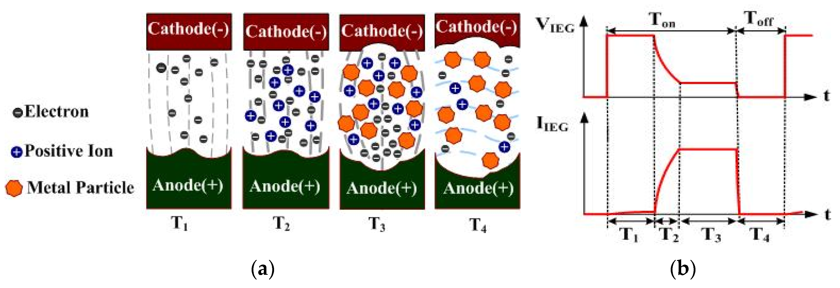
2.1. ESDM Principle
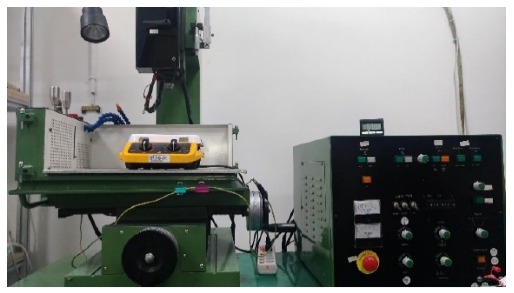
2.2. Existing-Micro-EDM System
2.3. Design of the Energy-Enhanced Micro-EDM System
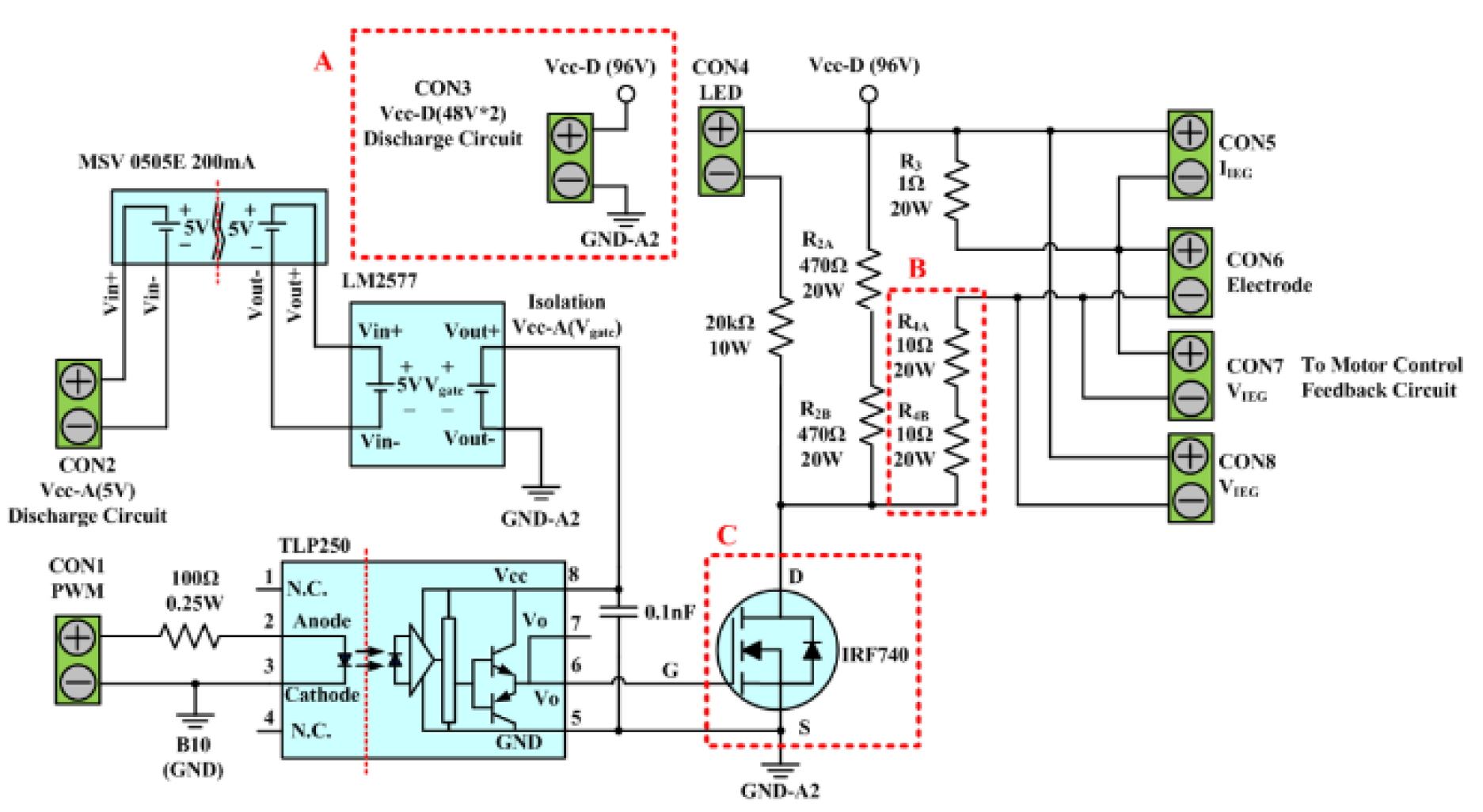
2.3.1. Discharge Circuit Design
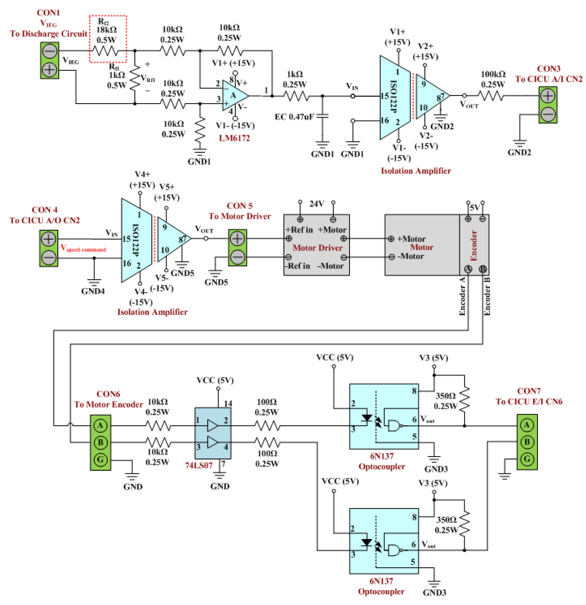
2.3.2. Motor Control Feedback Circuit Design
2.4. Nanoparticle-Size Analysis
3. Results
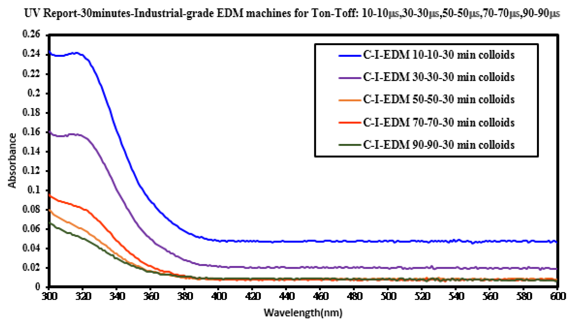
3.1. Property Analysis of the Nano-W Colloids Prepared Using the Industrial EDM
3.2. Property Analysis of Nano-W Colloids Prepared Using the ee-Micro-EDM System
3.3. Component Analysis of Nano-W Colloids
3.4. Property Comparison of Nano-W Colloids Prepared Using Industrial EDM and the ee-Micro-EDM System
4. Conclusions
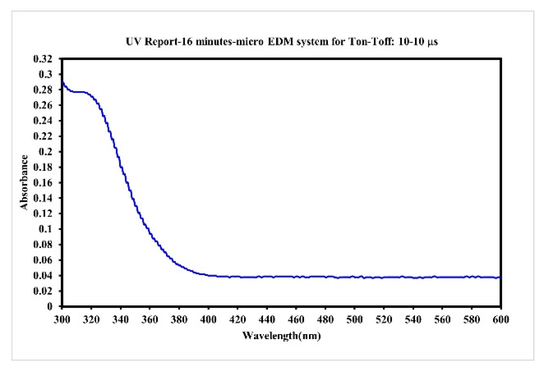
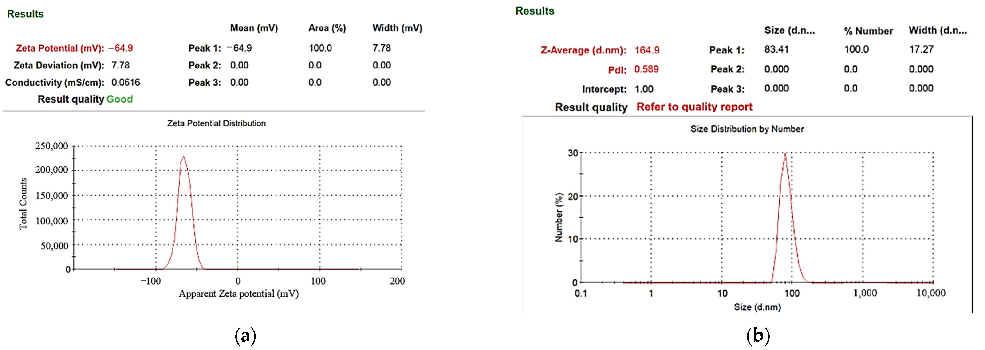
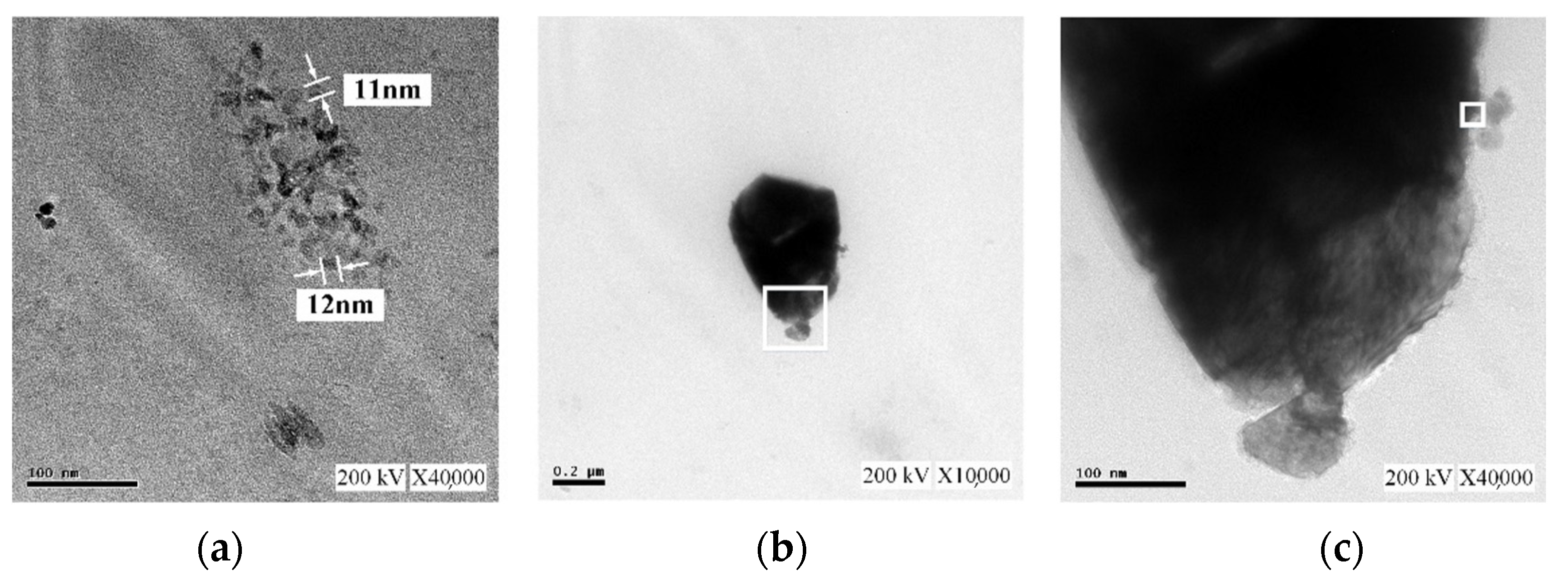
- Analysis using UV–Vis and a Zetasizer showed that the colloid prepared by the ee-micro-EDM system with a pulse on time and off time of 10–10 μs and a preparation time of 16 min had an absorbance of 0.277 at the wavelength of 315 nm, ζ potential of −64.9 mV, and an average particle size of 164.9 nm. TEM analysis showed that the particle size of this colloid was about 11–12 nm.
- Compared with the application of the industrial EDM system for nano-W colloid preparation, the ee-micro-EDM system has the advantages of a low cost, smaller size, and production of nano-W colloids with superior performance. Compared with the chemical preparation method for nano-W colloids, the ee-Micro-EDM system for preparing colloids does not permit nanoparticles to dissipate in the process environment. In summary, the ee-micro-EDM system represents an advanced technology for preparing high-quality nano-W colloids.
Author Contributions
Funding
Data Availability Statement
Conflicts of Interest
References
- Lee, S.; Li, X. Study of the effect of machining parameters on the machining characteristics in electrical discharge machining of tungsten carbide. J. Mater. Process. Technol. 2001, 115, 344–358. [Google Scholar] [CrossRef]
- Jahan, M.; Rahman, M.; Wong, Y. A review on the conventional and micro-electrodischarge machining of tungsten carbide. Int. J. Mach. Tools Manuf. 2011, 51, 837–858. [Google Scholar] [CrossRef]
- Colton, R.J.; Huang, J.-T.J.; Rabalais, J.W. Electronic structure of tungsten carbide and its catalytic behavior. Chem. Phys. Lett. 1975, 34, 337–339. [Google Scholar] [CrossRef]
- Claridge, J.B.; York, A.P.; Brungs, A.J.; Marquez-Alvarez, C.; Sloan, J.; Tsang, S.C.E.; Green, M.L.H. New Catalysts for the Conversion of Methane to Synthesis Gas: Molybdenum and Tungsten Carbide. J. Catal. 1998, 180, 85–100. [Google Scholar] [CrossRef]
- Chhina, H.; Campbell, S.; Kesler, O. Thermal and electrochemical stability of tungsten carbide catalyst supports. J. Power Sources 2007, 164, 431–440. [Google Scholar] [CrossRef]
- Gill, S.S.; Singh, J.; Singh, H.; Singh, R. Metallurgical and mechanical characteristics of cryogenically treated tungsten carbide (WC–Co). Int. J. Adv. Manuf. Technol. 2012, 58, 119–131. [Google Scholar] [CrossRef]
- Gotić, M.; Ivanda, M.; Popović, S.; Music, S. Synthesis of tungsten trioxide hydrates and their structural properties. Mater. Sci. Eng. B 2000, 77, 193–201. [Google Scholar] [CrossRef]
- Szilágyi, I.M.; Pfeifer, J.; Balázsi, C.; Tóth, A.L.; Varga-Josepovits, K.; Madarász, J.; Pokol, G. Thermal stability of hexagonal tungsten trioxide in air. J. Therm. Anal. 2008, 94, 499–505. [Google Scholar] [CrossRef]
- Hutchins, M.; Abu-Alkhair, O.; El-Nahass, M.; El-Hady, K.A. Structural and optical characterisation of thermally evaporated tungsten trioxide (WO3) thin films. Mater. Chem. Phys. 2006, 98, 401–405. [Google Scholar] [CrossRef]
- Patel, K.; Panchal, C.; Kheraj, V.; Desai, M. Growth, structural, electrical and optical properties of the thermally evaporated tungsten trioxide (WO3) thin films. Mater. Chem. Phys. 2009, 114, 475–478. [Google Scholar] [CrossRef]
- Meng, Z.; Fujii, A.; Hashishin, T.; Wada, N.; Sanada, T.; Tamaki, J.; Kojima, K.; Haneoka, H.; Suzuki, T. Morphological and crystal structural control of tungsten trioxide for highly sensitive NO2 gas sensors. J. Mater. Chem. C 2015, 3, 1134–1141. [Google Scholar] [CrossRef]
- Tomchenko, A.; Emelianov, I.; Khatko, V. Tungsten trioxide-based thick-film NO sensor: Design and investigation. Sensors Actuators B Chem. 1999, 57, 166–170. [Google Scholar] [CrossRef]
- Lu, T.; Chen, C.; Li, P.; Zhang, C.; Han, W.; Zhou, Y.; Suryanarayana, C.; Guo, Z. Enhanced mechanical and electrical properties of in situ synthesized nano-tungsten dispersion-strengthened copper alloy. Mater. Sci. Eng. A 2021, 799, 140161. [Google Scholar] [CrossRef]
- Dixit, S.; Kashyap, S.; Kailas, S.V.; Chattopadhyay, K. Manufacturing of high strength aluminium composites reinforced with nano tungsten particles for electrical application and investigation on in-situ reaction during processing. J. Alloys Compd. 2018, 767, 1072–1082. [Google Scholar] [CrossRef]
- Elsayed, A.; Li, W.; El Kady, O.A.; Daoush, W.M.; Olevsky, E.A.; German, R.M. Experimental investigations on the synthesis of W–Cu nanocomposite through spark plasma sintering. J. Alloys Compd. 2015, 639, 373–380. [Google Scholar] [CrossRef]
- Shi, H.; Magaye, R.; Castranova, V.; Zhao, J. Titanium dioxide nanoparticles: A review of current toxicological data. Part. Fibre Toxicol. 2013, 10, 15–33. [Google Scholar] [CrossRef] [Green Version]
- Shervani, Z.; Yamamoto, Y. Carbohydrate-directed synthesis of silver and gold nanoparticles: Effect of the structure of carbohydrates and reducing agents on the size and morphology of the composites. Carbohydr. Res. 2011, 346, 651–658. [Google Scholar] [CrossRef]
- Liao, C.-Y.; Tseng, K.-H.; Lin, H.-S. Preparation of Metallic Aluminum Compound Particles by Submerged Arc Discharge Method in Aqueous Media. Met. Mater. Trans. A 2013, 44, 91–97. [Google Scholar] [CrossRef]
- Tseng, K.-H.; Chou, C.-J.; Shih, S.-H.; Tien, D.-C.; Ku, H.-C.; Stobinski, L. Comparison of graphene impregnated with/without nanosilver prepared by submerged arc discharge method. Nanomater. Nanotechnol. 2018, 8, 1847980417752849. [Google Scholar] [CrossRef] [Green Version]
- Tseng, K.-H.; Lin, Z.-Y.; Chung, M.-Y.; Tien, D.-C.; Stobinski, L. Parameter control and property analysis in the preparation of platinum iodide nanocolloids through the electrical spark discharge method. RSC Adv. 2020, 10, 30169–30175. [Google Scholar] [CrossRef]
- Chen, L.; Mashimo, T.; Okudera, H.; Iwamoto, C.; Omurzak, E. Synthesis of WO3·H2O nanoparticles by pulsed plasma in liquid. RSC Adv. 2014, 4, 28673–28677. [Google Scholar] [CrossRef]
- Tseng, K.H.; Kao, Y.-S.; Chang, C.-Y. Development and Implementation of a Micro-electric Discharge Machine: Real-Time Monitoring System of Fabrication of Nanosilver Colloid. J. Clust. Sci. 2016, 27, 763–773. [Google Scholar] [CrossRef]
- Tseng, K.-H.; Chang, C.-Y.; Chen, M.-J.; Tseng, Y.-K. Novel electrical discharge machining system with real-time control and monitoring for preparing nanoiron colloid. Adv. Mech. Eng. 2018, 10, 1687814018791705. [Google Scholar] [CrossRef] [Green Version]
- Minhat, A.E.B.; Hj, N.H.B.; Yahya, A.B.; Andromeda, T.; Nugroho, K. Model of pulsed electrical discharge machining (EDM) using RL circuit. Int. J. Power Electron. Drive Syst. 2014, 5, 252. [Google Scholar] [CrossRef]
- Gostimirovic, M.; Kovac, P.; Sekulic, M.; Skoric, B. Influence of discharge energy on machining characteristics in EDM. J. Mech. Sci. Technol. 2012, 26, 173–179. [Google Scholar] [CrossRef]
- De Bruyn, H.E.; Pekelharing, A.J. Has the «Delay Time» Influence on the EDM-Process? CIRP Ann. 1982, 31, 103–106. [Google Scholar] [CrossRef]
- Yeo, S.H.; Tan, P.C.; Kurnia, W. Effects of powder additives suspended in dielectric on crater characteristics for micro electrical discharge machining. J. Micromech. Microeng. 2007, 17, N91–N98. [Google Scholar] [CrossRef]
- Tseng, K.-H.; Lin, Y.-S.; Chang, C.-Y.; Chung, M.-Y. A Study of a PID Controller Used in a Micro-Electrical Discharge Machining System to Prepare TiO2 Nanocolloids. Nanomaterials 2020, 10, 1044. [Google Scholar] [CrossRef]
- Gołdasz, J.; Sapinski, B.; Jastrzębski, Ł. Assessment of the Magnetic Hysteretic Behaviour of MR Dampers through Sensorless Measurements. Shock Vib. 2018, 2018, 3740208. [Google Scholar] [CrossRef]
- Toma, E.; Simion, C. The improvement of edm pulse generator performances by use of the news silicon-carbide mos transistors. Rev. De Tehnol. Neconv. 2016, 20, 28. [Google Scholar]
- Erawan, M.A.; Yahya, A.; Hisham, K.N.; Samosir, A.S.; Rahim, M.A.A.; Trias, A.; Kartiko, J.P.N. Model of Pulse Power Generator in Electrical Discharge Machining (EDM) System. Appl. Mech. Mater. 2014, 554, 613–617. [Google Scholar] [CrossRef]
- Hashim, N.L.S.; Yahya, A.; Daud, M.; Samion, S.; Baharom, A.; Haji Khamis, N.H.; Mahmud, N. A Review on Electrical Discharge Machining Servomechanism System. Sci. Iran. 2015, 22, 1813–1832. [Google Scholar]
- Andromeda, T.; Yahya, A.; Samion, S.; Baharom, A.; Hashim, N.L. Differential evolution for optimization of pid gain in electrical discharge machining control system. Trans. Can. Soc. Mech. Eng. 2013, 37, 293–301. [Google Scholar] [CrossRef]
- Babu, R.; Swarnalatha, R. Comparison of Different Tuning Methods for pH Neutralization in Textile Industry. J. Appl. Sci. 2017, 17, 142–147. [Google Scholar] [CrossRef]
- Hashim, N.L.S.; Yahya, A.; Andromeda, T.; Kadir, M.R.R.A.; Mahmud, N.; Samion, S. Simulation of PSO-PI Co ontroller of DC Motor in Micro--EDM System for Biomedical Application. Procedia Eng. 2012, 41, 805–811. [Google Scholar] [CrossRef] [Green Version]
- Abu Qudeiri, J.E.; Zaiout, A.; Mourad, A.-H.I.; Abidi, M.H.; Elkaseer, A. Principles and Characteristics of Different EDM Processes in Machining Tool and Die Steels. Appl. Sci. 2020, 10, 2082. [Google Scholar] [CrossRef] [Green Version]
- Kumar, A.; Mandal, A.; Dixit, A.R.; Das, A.K.; Kumar, S.; Ranjan, R. Comparison in the performance of EDM and NPMEDM using Al2O3 nanopowder as an impurity in DI water dielectric. Int. J. Adv. Manuf. Technol. 2019, 100, 1327–1339. [Google Scholar] [CrossRef]
- Bhaumik, M.; Maity, K. Effect of Electrode Materials on Different EDM Aspects of Titanium Alloy. Silicon 2019, 11, 187–196. [Google Scholar] [CrossRef]


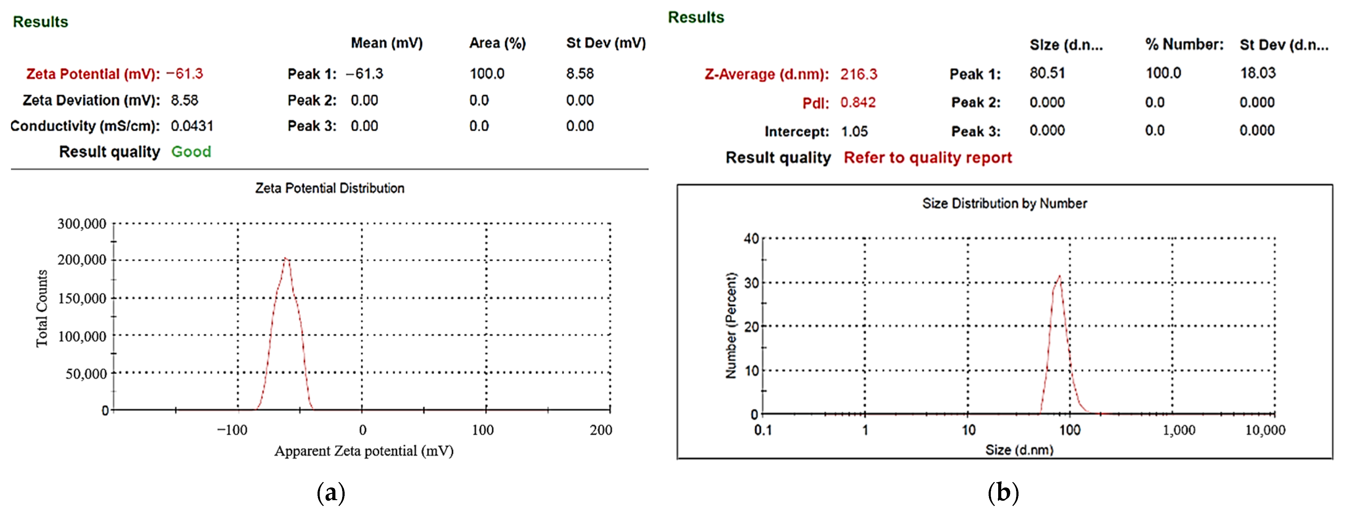
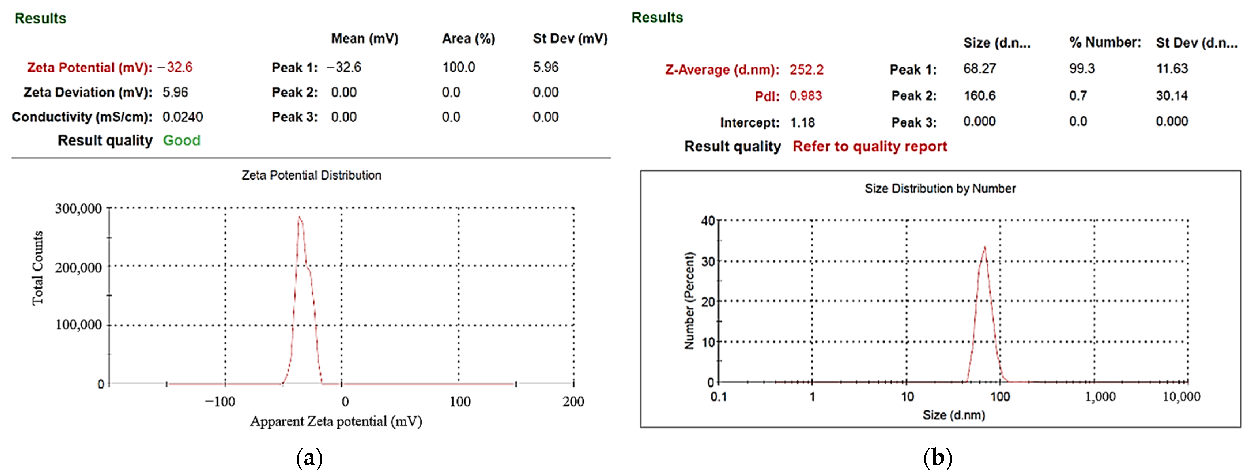
| Colloid | C-I-EDM 10-10-30 min Colloids | C-I-EDM 30-30-30 min Colloids |
|---|---|---|
| Wavelength | 316 nm | 315 nm |
| Absorbance peak | 0.242 | 0.158 |
| ζ potential | −61.3mV | −32.6mV |
| PDI | 0.842 | 0.983 |
| Average particle size | 216.3 nm | 252.2 nm |
| Particle size distribution at peak 1 | 80.51 nm | 68.27 nm |
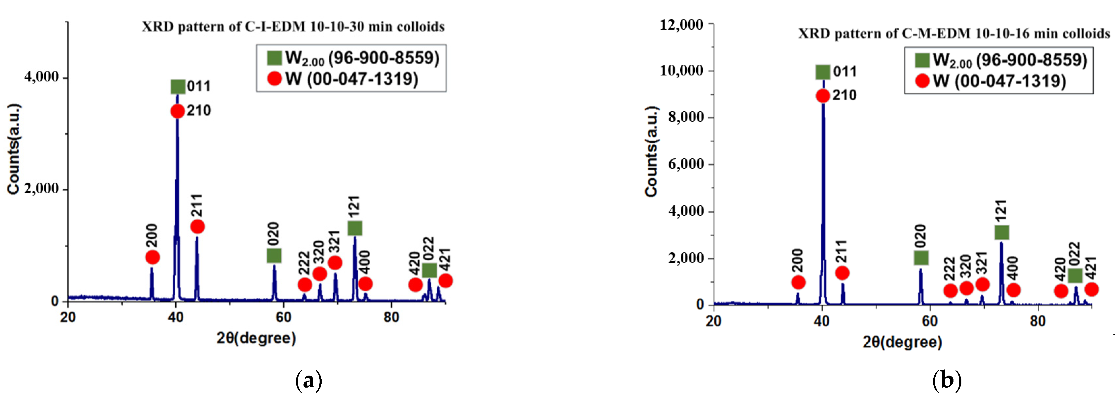
| Compound Name | Chem. Formula | The Positions 2θ and Miller Indices (h k l) |
|---|---|---|
| Tungsten | 40.2° (0 1 1) 58.2° (0 2 0) 73.1° (1 2 1) 87.0° (0 2 2) | |
| Tungsten | W | 35.5° (2 0 0) 39.8° (2 1 0) 43.8° (2 1 1) 63.7° (2 2 2) 66.7° (3 2 0) 69.6° (3 2 1) 75.1° (4 0 0) 86.0° (4 2 0) 88.6° (4 2 1) |
| Colloid | C-I-EDM 10-10-30 min Colloids | C-M-EDM 10-10-16 min Colloids |
|---|---|---|
| Wavelength | 316 nm | 315 nm |
| Absorbance peak | 0.242 | 0.277 |
| Preparation time | 30 min | 16 min |
| ζ potential | −61.3 mV | −64.9 mV |
| Average particle size | 216.3 nm | 164.9 nm |
| PDI | 0.842 | 0.589 |
| Particle size distribution at peak 1 | 80.51 nm | 83.41 nm |
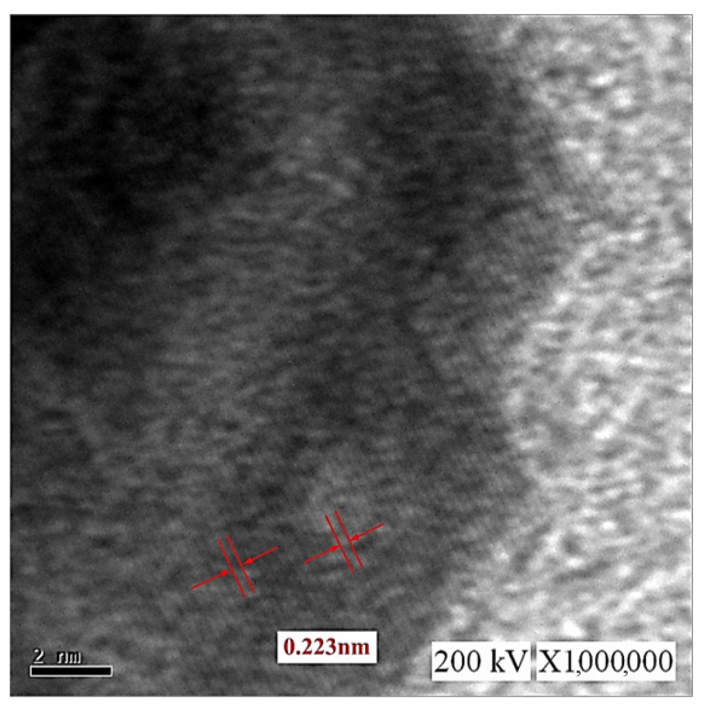
| Lattice line width | 0.223 nm | 0.223 nm |
| Particle appearance and morphology | 80 nm, quadrangle particle shape | 11–12 nm, irregular particle shape |
Publisher’s Note: MDPI stays neutral with regard to jurisdictional claims in published maps and institutional affiliations. |
© 2022 by the authors. Licensee MDPI, Basel, Switzerland. This article is an open access article distributed under the terms and conditions of the Creative Commons Attribution (CC BY) license (https://creativecommons.org/licenses/by/4.0/).
Share and Cite
Chang, C.-Y.; Tseng, K.-H.; Chang, J.-T.; Chung, M.-Y.; Lin, Z.-Y. A Study of Nano-Tungsten Colloid Preparing by the Electrical Spark Discharge Method. Micromachines 2022, 13, 2009. https://doi.org/10.3390/mi13112009
Chang C-Y, Tseng K-H, Chang J-T, Chung M-Y, Lin Z-Y. A Study of Nano-Tungsten Colloid Preparing by the Electrical Spark Discharge Method. Micromachines. 2022; 13(11):2009. https://doi.org/10.3390/mi13112009
Chicago/Turabian StyleChang, Chaur-Yang, Kuo-Hsiung Tseng, Jui-Tsun Chang, Meng-Yun Chung, and Zih-Yuan Lin. 2022. "A Study of Nano-Tungsten Colloid Preparing by the Electrical Spark Discharge Method" Micromachines 13, no. 11: 2009. https://doi.org/10.3390/mi13112009