
Metasurfaces as Energy Valves for Sustainable Energy Management


Abstract
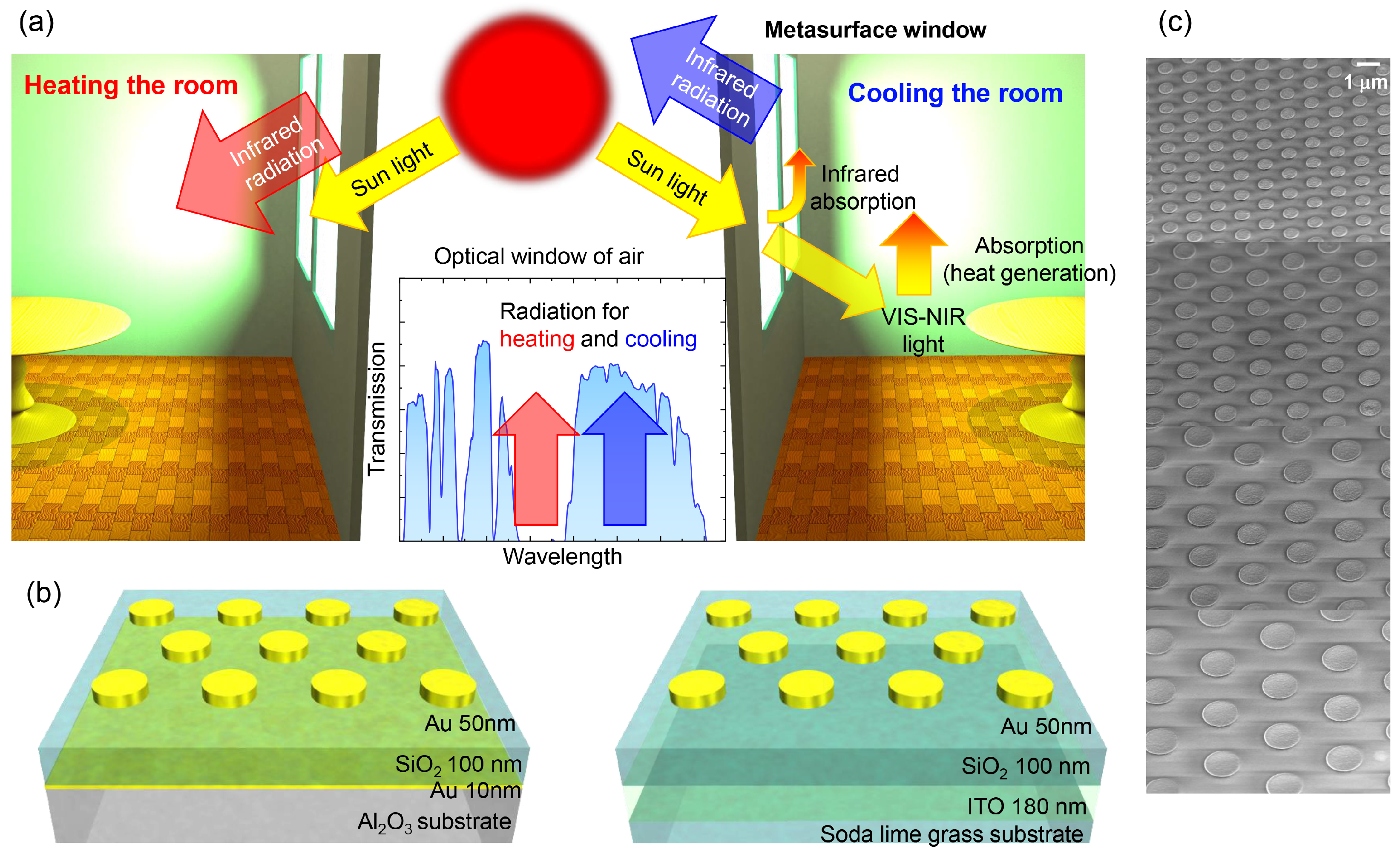
:1. Introduction
2. Experimental Procedures and Modeling
2.1. Fabrication of Transparent Metasurfaces
2.2. Optical Characterization
2.3. FDTD Simulation of MIM Properties
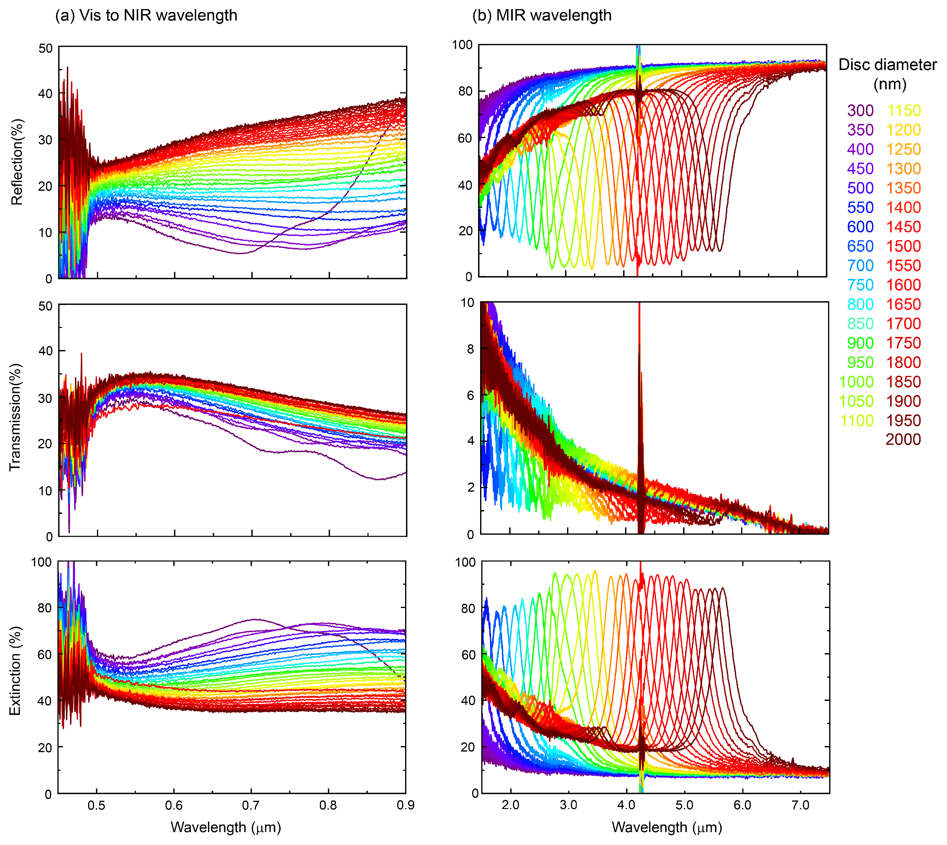
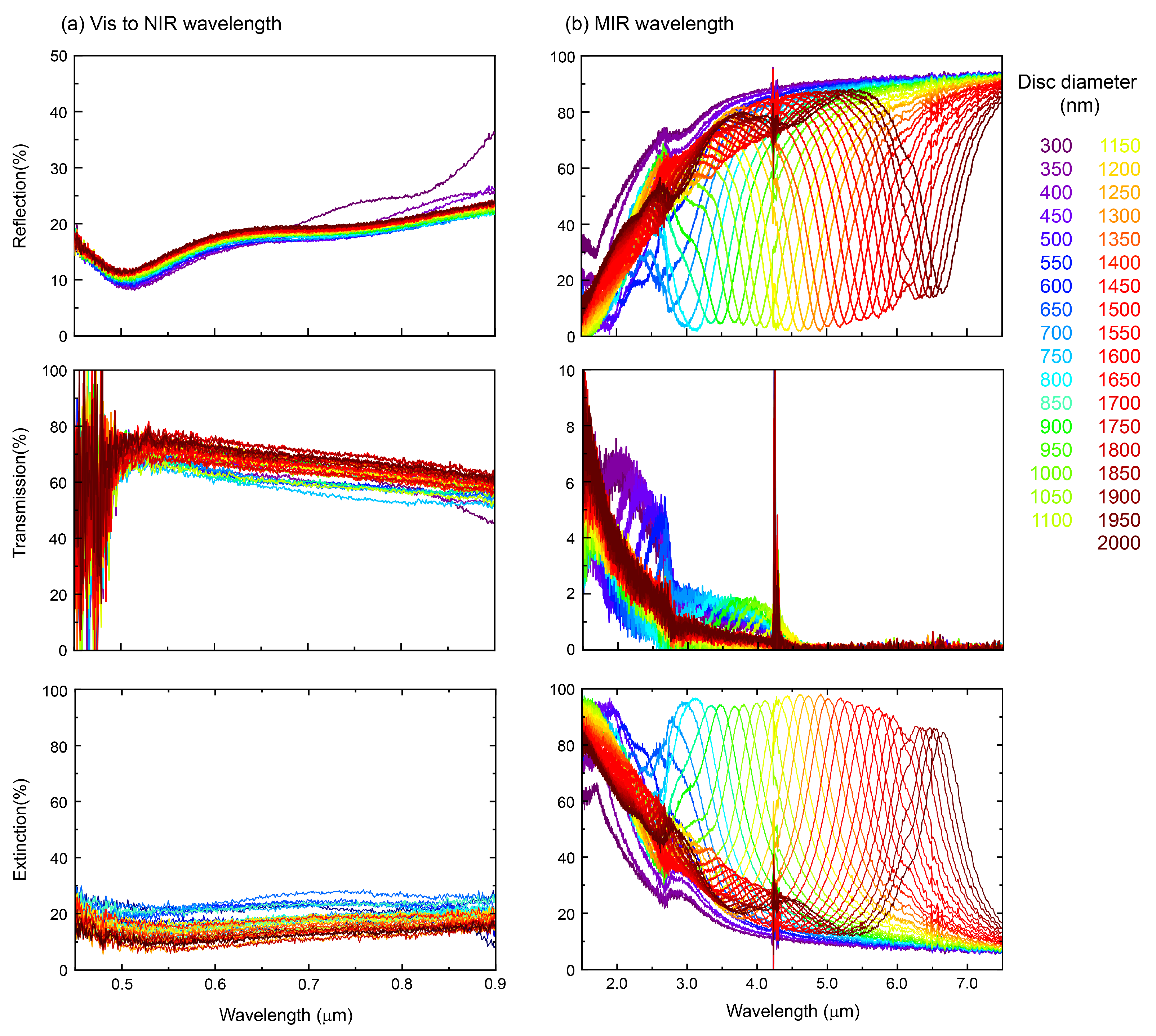
3. Results and Discussion
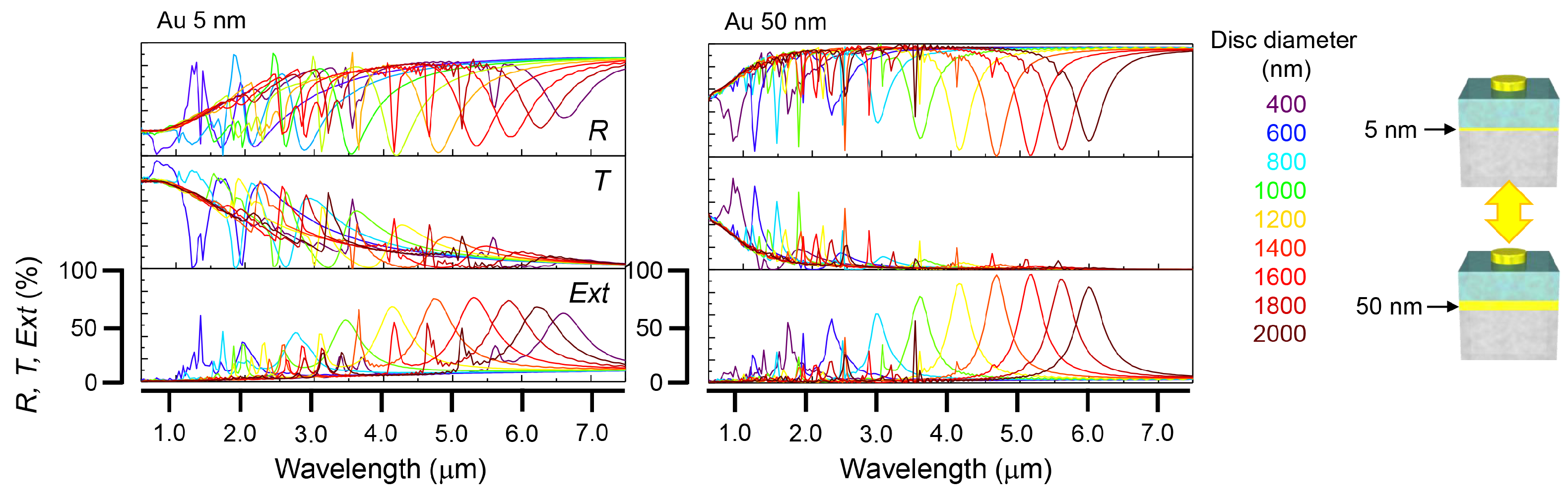
3.1. Thin Au as a Metal Base in MIM Metasurface
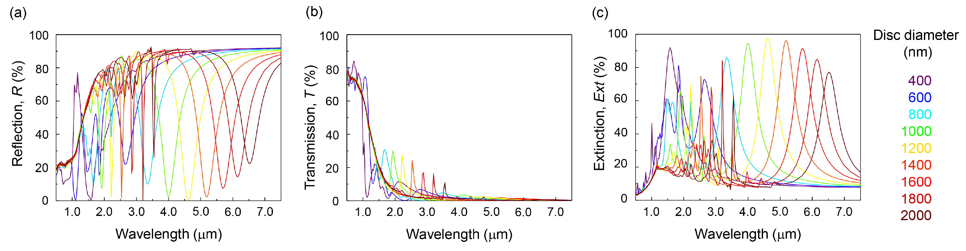
3.2. ITO as a Metal Base in MIM Metasurface
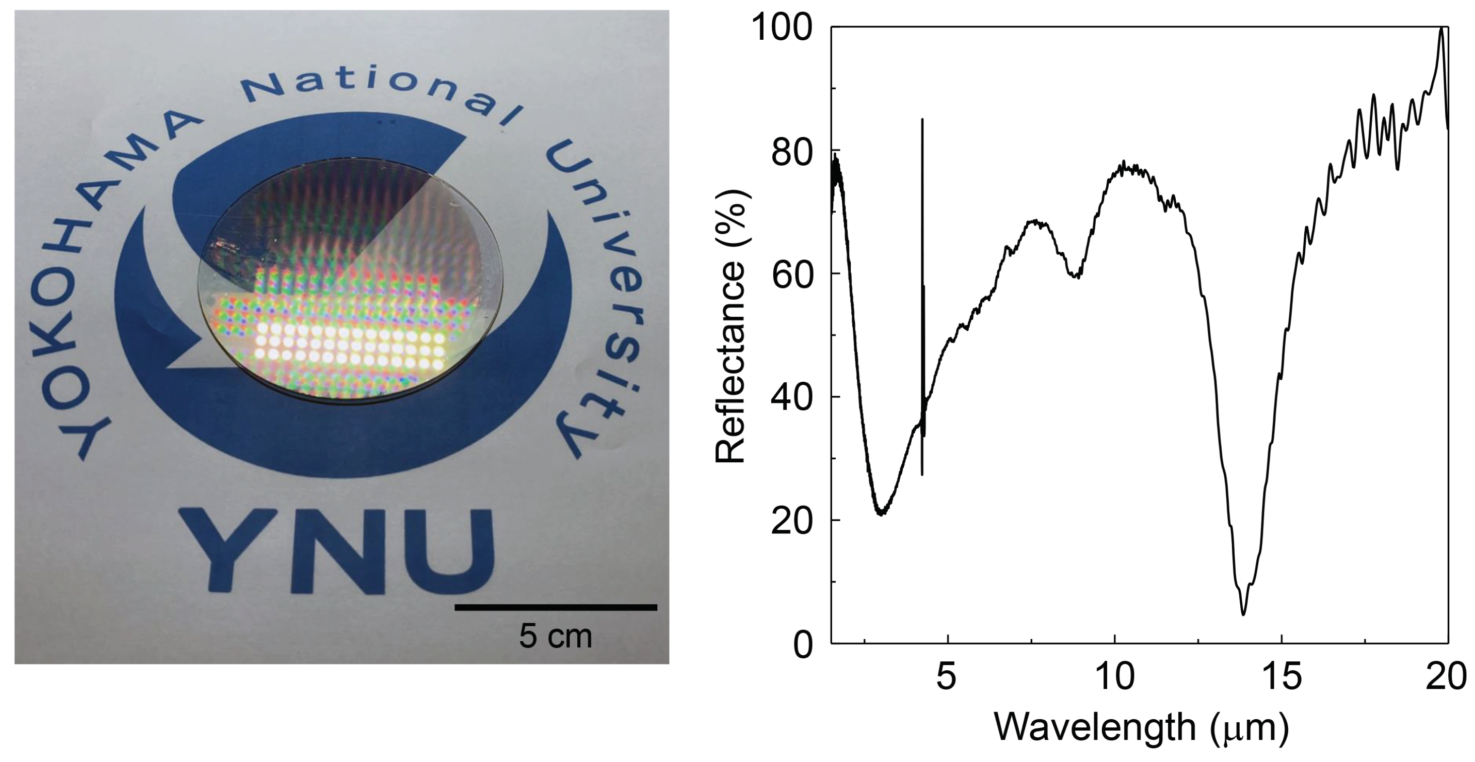
3.3. Large-Area Fabrication for Radiation Control (an Optical Window)
4. Conclusions
Supplementary Materials
Author Contributions
Funding
Data Availability Statement
Conflicts of Interest
References
- Sreekanth, K.V.; Alapan, Y.; Ilker, M.E.E.; Hinczewski, M.; Gurkan, U.A.; Luca, A.D.; Strangi, G. Extreme sensitivity biosensing platform based on hyperbolic metamaterials. Nat. Mater. 2016, 15, 621–627. [Google Scholar] [CrossRef] [PubMed] [Green Version]
- Monticone, F.; Alu, A. Invisibility exposed: Physical bounds on passive cloaking. Optica 2016, 3, 718–724. [Google Scholar] [CrossRef]
- Kuttruff, J.; Gabbani, A.; Petrucci, G.; Zhao, Y.; Iarossi, M.; Pedrueza-Villalmanzo, E.; Dmitriev, A.; Parracino, A.; Strangi, G.; Angelis, F.D.; et al. Magneto-Optical Activity in Nonmagnetic Hyperbolic Nanoparticles. Phys. Rev. Lett. 2021, 127, 217402. [Google Scholar] [CrossRef]
- Zhao, B.; Guo, C.; Garcia, C.A.C.; Narang, P.; Fan, S. Axion-Field-Enabled Nonreciprocal Thermal Radiation in Weyl Semimetals. Nano Lett. 2020, 20, 1923–1927. [Google Scholar] [CrossRef] [PubMed]
- Lim, M.; Song, J.; Lee, S.S.; Lee, J.; Lee, B.J. Surface-Plasmon-Enhanced Near-Field Radiative Heat Transfer between Planar Surfaces with a Thin-Film Plasmonic Coupler. Phys. Rev. Appl. 2020, 14, 014070. [Google Scholar] [CrossRef]
- Barho, F.B.; Gonzalez-Posada, F.; Cerutti, L.; Taliercio, T. Heavily Doped Semiconductor Metamaterials for Mid-Infrared Multispectral Perfect Absorption and Thermal Emission. Adv. Opt. Mater. 2020, 8, 1901502. [Google Scholar] [CrossRef]
- Berquist, Z.J.; Turaczy, K.K.; Lenert, A. Plasmon-enhanced greenhouse selectivity for high-temperature solar thermal energy conversion. ACS Nano 2020, 14, 12605–12613. [Google Scholar] [CrossRef]
- Yada, K.; Sakurai, A. Active thermal radiation control with nanoslit graphene metasurface. J. Quant. Spectrosc. Radiat. Transf. 2021, 260, 107450. [Google Scholar] [CrossRef]
- Shi, K.; Sun, Y.; Chen, Z.; He, N.; Bao, F.; Evans, J.; He, S. Colossal Enhancement of Near-Field Thermal Radiation across Hundreds of Nanometers between Millimeter-Scale Plates through Surface Plasmon and Phonon Polaritons Coupling. Nano Lett. 2019, 19, 8082–8088. [Google Scholar] [CrossRef] [PubMed]
- Cao, T.; Zhang, X.; Dong, W.; Lu, L.; Zhou, X.; Zhuang, X.; Deng, J.; Cheng, X.; Li, G.; Simpson, R.E. Tuneable Thermal Emission Using Chalcogenide Metasurface. Adv. Opt. Mater. 2018, 6, 1800169. [Google Scholar] [CrossRef]
- Li, W.; Fan, S. Nanophotonic control of thermal radiation for energy applications. Opt. Express 2018, 26, 15995. [Google Scholar] [CrossRef] [PubMed]
- Ma, R.; Wu, D.; Liu, Y.; Ye, H.; Sutherland, D. Copper plasmonic metamaterial glazing for directional thermal energy management. Mater. Des. 2020, 188, 108407. [Google Scholar] [CrossRef]
- Kang, Q.; Li, D.; Guo, K.; Gao, J.; Guo, Z. Tunable Thermal Camouflage Based on GST Plasmonic Metamaterial. Nanomaterials 2021, 11, 260. [Google Scholar] [CrossRef] [PubMed]
- Song, J.; Huang, S.; Ma, Y.; Cheng, Q.; Hu, R.; Luo, X. Radiative metasurface for thermal camouflage, illusion and messaging. Opt. Express 2020, 28, 875. [Google Scholar] [CrossRef] [PubMed]
- Zhang, Y.; Wang, C.H.; Yi, H.L.; Tan, H.P. Multiple surface plasmon polaritons mediated near-field radiative heat transfer between graphene/vacuum multilayers. J. Quant. Spectrosc. Radiat. Transf. 2018, 221, 138–146. [Google Scholar] [CrossRef]
- Kondo, T.; Hasegawa, S.; Yanagishita, T.; Kimura, N.; Toyonaga, T.; Masuda, H. Control of thermal radiation in metal hole array structures formed by anisotropic anodic etching of Al. Opt. Express 2018, 26, 27865. [Google Scholar] [CrossRef] [PubMed]
- Yang, J.; Du, W.; Su, Y.; Fu, Y.; Gong, S.; He, S.; Ma, Y. Observing of the super-Planckian near-field thermal radiation between graphene sheets. Nat. Commun. 2018, 9, 4033. [Google Scholar] [CrossRef] [PubMed] [Green Version]
- Ryu, M.; Nishijima, Y.; Morimoto, S.; To, N.; Hashizume, T.; Matsubara, R.; Kubono, A.; Hu, J.; Ng, S.H.; Juodkazis, S.; et al. Hyperspectral Molecular Orientation Mapping in Metamaterials. Appl. Sci. 2021, 11, 1544. [Google Scholar] [CrossRef]
- Beni, T.; Yamasaku, N.; Kurotsu, T.; To, N.; Okazaki, S.; Arakawa, T.; Balcytis, A.; Seniutinas, G.; Juodkazis, S.; Nishijima, Y. Metamaterial for Hydrogen Sensing. ACS Sens. 2019, 4, 2389–2394. [Google Scholar] [CrossRef] [PubMed]
- Kumagai, T.; To, N.; Balcytis, A.; Seniutinas, G.; Juodkazis, S.; Nishijima, Y. Kirchhoff’s Thermal Radiation from Lithography-Free Black Metals. Micromachines 2020, 11, 824. [Google Scholar] [CrossRef]
- Lundgaard, S.; Ng, S.H.; Nishijima, Y.; Mazilu, M.; Juodkazis, S. Black Metals: Optical Absorbers. Micromachines 2020, 11, 256. [Google Scholar] [CrossRef] [PubMed] [Green Version]
- Nishijima, Y.; Morimoto, S.; Balcytis, A.; Hashizume, T.; Matsubara, R.; Kubono, A.; To, N.; Meguya, R.; Morikawa, J.; Juodkazis, S. Efficient molecular emitter. J. Mater. Chem. C 2022, 10, 451–462. [Google Scholar] [CrossRef]
- To, N.; Juodkazis, S.; Nishijima, Y. Detailed Experiment- Theory Comparison of Mid-Infrared Metasurface Perfect Absorbers. Micromachines 2020, 11, 409. [Google Scholar] [CrossRef] [PubMed] [Green Version]
- Nishijima, Y.; Balcytis, A.; Naganuma, S.; Seniutinas, G.; Juodkazis, S. Kirchhoff’s metasurfaces towards efficient photo-thermal energy conversion. Sci. Rep. 2019, 9, 8284. [Google Scholar] [CrossRef] [PubMed] [Green Version]
- Nishijima, Y.; Balcytis, A.; Naganuma, S.; Seniutinas, G.; Juodkazis, S. Tailoring Metal and Insulator Contri- butions in Plasmonic Perfect Absorber Metasurfaces. ACS Appl. Nano Mater. 2018, 1, 3557–3564. [Google Scholar] [CrossRef]
- Raman, A.P.; Anoma, M.A.; Zhu, L.; Rephaeli, E.; Fan, S. Passive radiative cooling below ambient air temperature under direct sunlight. Nature 2014, 515, 540–544. [Google Scholar] [CrossRef] [PubMed]
- Kusnandar, K.; Brazier, F.M.; van Kooten, O. Empowering change for sustainable agriculture: The need for participation. Int. J. Agric. Sustain. 2019, 17, 271–286. [Google Scholar] [CrossRef] [Green Version]
- Shrestha, S.; Wang, Y.; Overvig, A.C.; Lu, M.; Stein, A.; Dal Negro, L.; Yu, N. Indium Tin Oxide Broadband Metasurface Absorber. ACS Photonics 2018, 5, 3526–3533. [Google Scholar] [CrossRef]
- Modi, K.S.; Kaur, J.; Singh, S.P.; Tiwari, U.; Sinha, R.K. Extremely high figure of merit in all-dielectric split asymmetric arc metasurface for refractive index sensing. Opt. Commun. 2020, 462, 125327. [Google Scholar] [CrossRef]
- Ramarajan, R.; Kovendhan, M.; Thangaraju, K.; Joseph, D.P.; Babu, R.R.; Elumalai, V. Enhanced optical transparency and electrical conductivity of Ba and Sb co-doped SnO2 thin films. J. Alloy. Compd. 2020, 823, 153709. [Google Scholar] [CrossRef]
- Safari, M.; Kherani, N.P.; Eleftheriades, G.V. Multi-Functional Metasurface: Visibly and RF Transparent, NIR Control and Low Thermal Emissivity. Adv. Opt. Mater. 2021, 9, 2100176. [Google Scholar] [CrossRef]
- Yan, Z.; Bao, J.; Yue, X.Y.; Li, X.L.; Zhou, Y.N.; Wu, X.J. Impacts of preparation conditions on photoelectric properties of the ZnO:Ge transparent conductive thin films fabricated by pulsed laser deposition. J. Alloy. Compd. 2020, 812, 152093. [Google Scholar] [CrossRef]
- Okatani, T.; Abe, Y.; Nakazawa, T.; Hane, K.; Kanamori, Y. Fabrication of silicon nanospheres placeable on a desired position for dielectric metamaterials in the visible region. Opt. Mater. Express 2021, 11, 189. [Google Scholar] [CrossRef]
- Lopez-Santos, C.; Puerto, D.; Siegel, J.; Macias-Montero, M.; Florian, C.; Gil-Rostra, J.; López-Flores, V.; Borras, A.; González-Elipe, A.R.; Solis, J. Anisotropic Resistivity Surfaces Produced in ITO Films by Laser-Induced Nanoscale Self-organization. Adv. Opt. Mater. 2021, 9, 2001086. [Google Scholar] [CrossRef]
- Kim, J.H.; Seong, T.Y.; Ahn, K.J.; Chung, K.B.; Seok, H.J.; Seo, H.J.; Kim, H.K. The effects of film thickness on the electrical, optical, and structural properties of cylindrical, rotating, magnetron-sputtered ITO films. Appl. Surf. Sci. 2018, 440, 1211–1218. [Google Scholar] [CrossRef]
- Li, Y.T.; Chen, D.T.; Han, C.F.; Lin, J.F. Effect of the addition of zirconium on the electrical, optical, and mechanical properties and microstructure of ITO thin films. Vacuum 2021, 183, 109844. [Google Scholar] [CrossRef]
- Hsueh, T.J.; Peng, C.H.; Chen, W.S. A transparent ZnO nanowire MEMS gas sensor prepared by an ITO micro-heater. Sens. Actuators B Chem. 2020, 304, 127319. [Google Scholar] [CrossRef]
- Chai, X.; Zhang, Y.; Cao, Y.; Wu, L.; Ma, J.; Liu, Y.; Song, L. Modulation of photoelectric properties of indium tin oxide thin films via oxygen control, and its application to epsilon-near-zero properties for an infrared absorber. J. Appl. Phys. 2020, 128, 185301. [Google Scholar] [CrossRef]
- Yildirim, D.U.; Ghobadi, A.; Soydan, M.C.; Atesal, O.; Toprak, A.; Caliskan, M.D.; Ozbay, E. Disordered and Densely Packed ITO Nanorods as an Excellent Lithography-Free Optical Solar Reflector Metasurface. ACS Photonics 2019, 6, 1812–1822. [Google Scholar] [CrossRef] [Green Version]
- Zhang, S.; Wang, T.; Lin, S.; Zhang, Y.; Tesfamichael, T.; Bell, J.; Wang, H. Effect of different thermo-treatment at relatively low temperatures on the properties of indium tin oxide thin films. Thin Solid Film. 2017, 636, 702–709. [Google Scholar] [CrossRef]
- Ali, H.M.; Mohamed, H.A.; Mohamed, S.H. Enhancement of the optical and electrical properties of ITO thin films deposited by electron beam evaporation technique. EPJ Appl. Phys. 2005, 31, 87–93. [Google Scholar] [CrossRef]
- Shirmanesh, G.K.; Sokhoyan, R.; Pala, R.A.; Atwater, H.A. Dual-Gated Active Metasurface at 1550 nm with Wide (>300°) Phase Tunability. Nano Lett. 2018, 18, 2957–2963. [Google Scholar] [CrossRef] [PubMed]
- Wolf, N.; Gerstenlauer, D.; Manara, J. Modelling the spectral reflectances of miscellaneous ITO coatings by using only the Drude theory. J. Phys. Conf. Ser. 2012, 395, 012064. [Google Scholar] [CrossRef]
- Nishijima, Y.; To, N.; Balcytis, A.; Juodkazis, S. Absorption and scattering in perfect thermal radiation absorber-emitter metasurfaces. Optics Express 2022, 30, 4058–4070. [Google Scholar] [CrossRef] [PubMed]
- Kravets, V.G.; Kabashin, A.V.; Barnes, W.L.; Grigorenko, A.N. Plasmonic Surface Lattice Resonances: A Review of Properties and Applications. Chem. Rev. 2018, 118, 5912–5951. [Google Scholar] [CrossRef]
- Nishijima, Y.; Rosa, L.; Juodkazis, S. Surface plasmon resonances in periodic and random patterns of gold nano-discs for broadband light harvesting. Opt. Express 2012, 20, 11466–11477. [Google Scholar] [CrossRef]
- Ishibashi, S.; Higuchi, Y.; Ota, Y.; Nakamura, K. Low resistivity indium-tin oxcide transparent conductive films. II. Effect of sputtering voltage on electrical property of films. J. Vac. Sci. Technol. A 1990, 8, 1403–1406. [Google Scholar] [CrossRef]
- Katsonis, N.; Kudernac, T.; Walko, M.; van der Molen, S.J.; van Wees, B.J.; Feringa, B.L. Reversible Conductance Switching of Single Diarylethenes on a Gold Surface. Adv. Mater. 2006, 18, 1397–1400. [Google Scholar] [CrossRef]
- Ray, S.; Banerjee, R.; Basu, N.; Batabyal, A.K.; Barua, A.K. Properties of tin doped indium oxide thin films prepared by magnetron sputtering. J. Appl. Phys. 1983, 54, 3497. [Google Scholar] [CrossRef]
- Ohhata, Y.; Shinoki, F.; Yoshida, S. Optical properties of r.f. reactive sputtered tin-doped In2O3 films. Thin Solid Film. 1979, 59, 255–261. [Google Scholar] [CrossRef]
- Kecebas, M.A.; Menguc, M.P.; Kosar, A.; Sendur, K. Passive radiative cooling design with broadband optical thin-film filters. J. Quant. Spectrosc. Radiat. Transf. 2017, 198, 179–186. [Google Scholar] [CrossRef]
- Santamouris, M.; Feng, J. Recent Progress in Daytime Radiative Cooling: Is It the Air Conditioner of the Future? Buildings 2018, 8, 168. [Google Scholar] [CrossRef]


Publisher’s Note: MDPI stays neutral with regard to jurisdictional claims in published maps and institutional affiliations. |
© 2022 by the authors. Licensee MDPI, Basel, Switzerland. This article is an open access article distributed under the terms and conditions of the Creative Commons Attribution (CC BY) license (https://creativecommons.org/licenses/by/4.0/).
Share and Cite
Nishijima, Y.; Kimura, S.; Takeshima, Y.; Juodkazis, S. Metasurfaces as Energy Valves for Sustainable Energy Management. Micromachines 2022, 13, 1769. https://doi.org/10.3390/mi13101769
Nishijima Y, Kimura S, Takeshima Y, Juodkazis S. Metasurfaces as Energy Valves for Sustainable Energy Management. Micromachines. 2022; 13(10):1769. https://doi.org/10.3390/mi13101769
Chicago/Turabian StyleNishijima, Yoshiaki, Syunya Kimura, Yu Takeshima, and Saulius Juodkazis. 2022. "Metasurfaces as Energy Valves for Sustainable Energy Management" Micromachines 13, no. 10: 1769. https://doi.org/10.3390/mi13101769