
AFM Nanotribomechanical Characterization of Thin Films for MEMS Applications


Abstract
:1. Introduction


2. AFM Measurement Technique for Tribological Characterization of Thin Film Materials
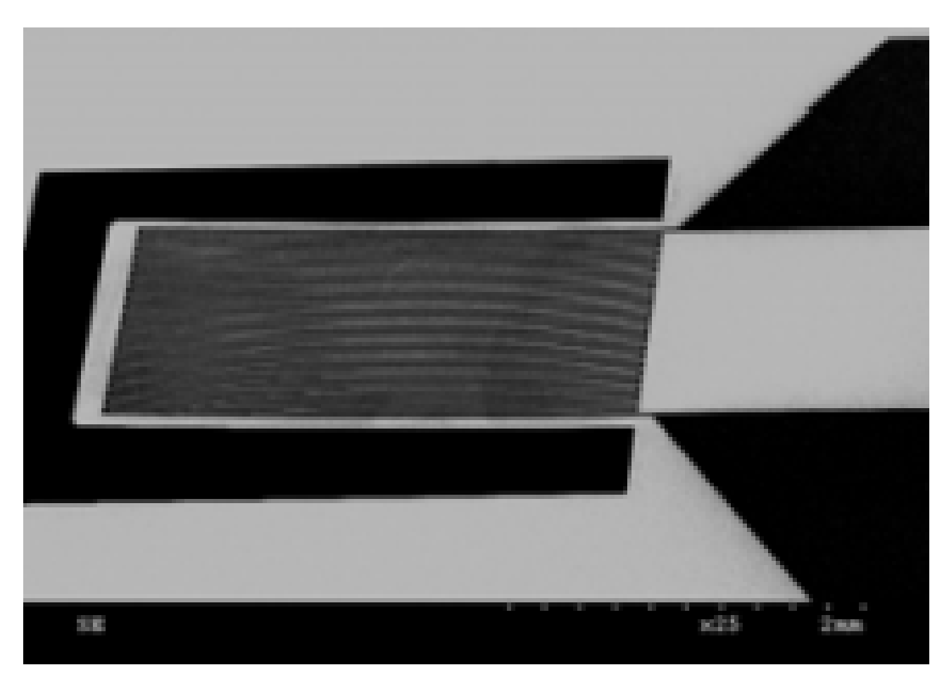
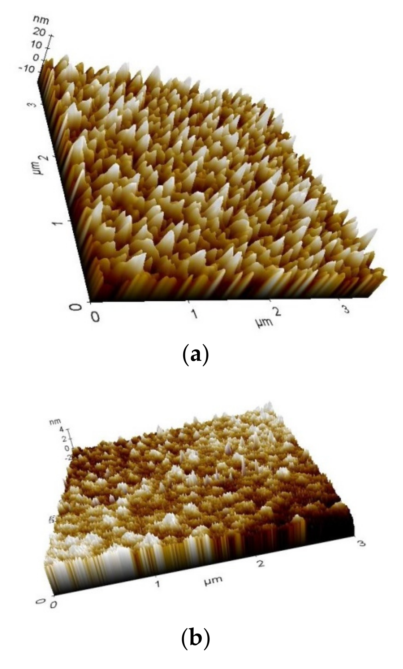
2.1. Basic Topographic Imaging
2.2. Mapping of the Frictional Force: Lateral Force Microscopy (LFM)
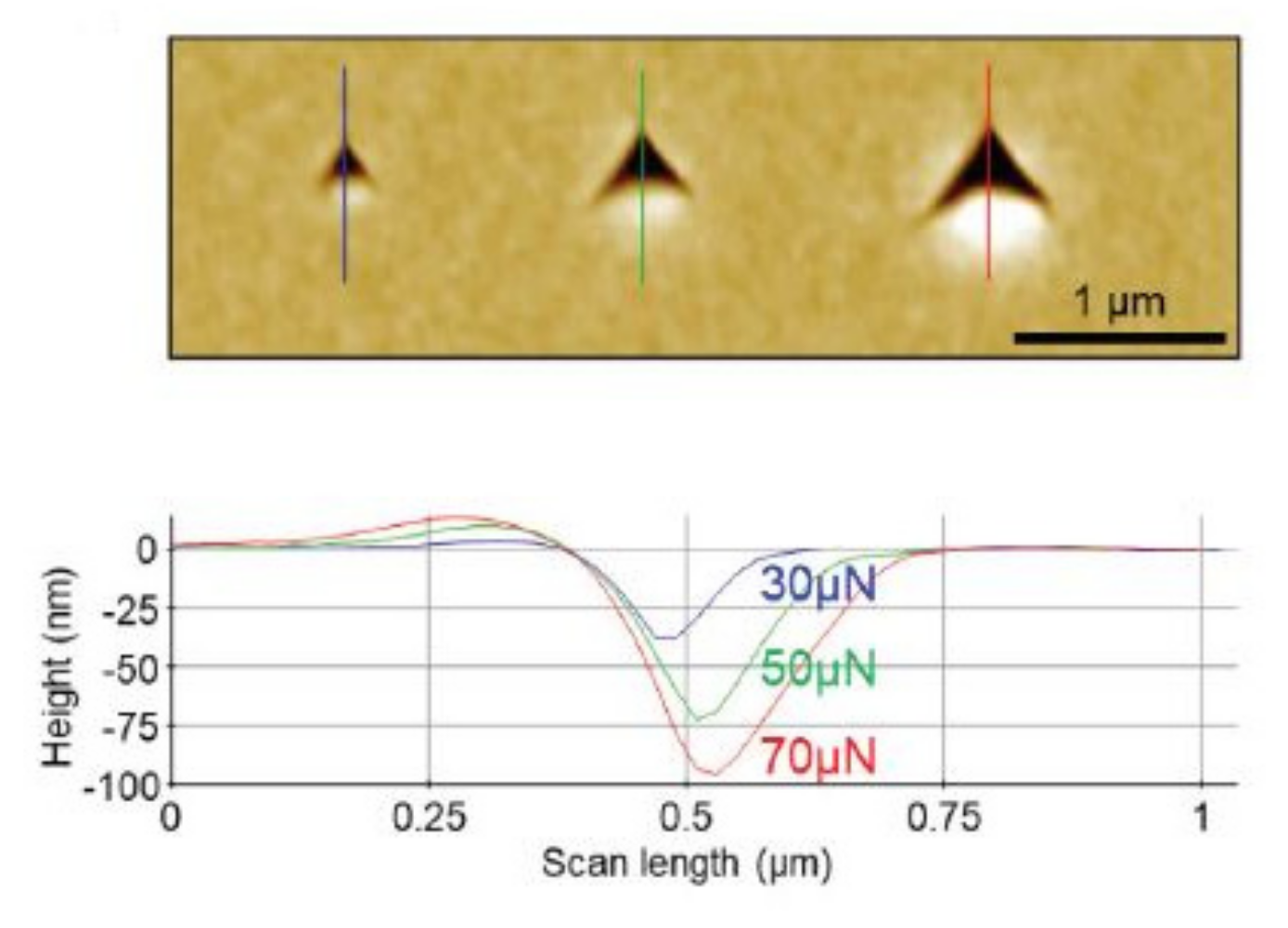
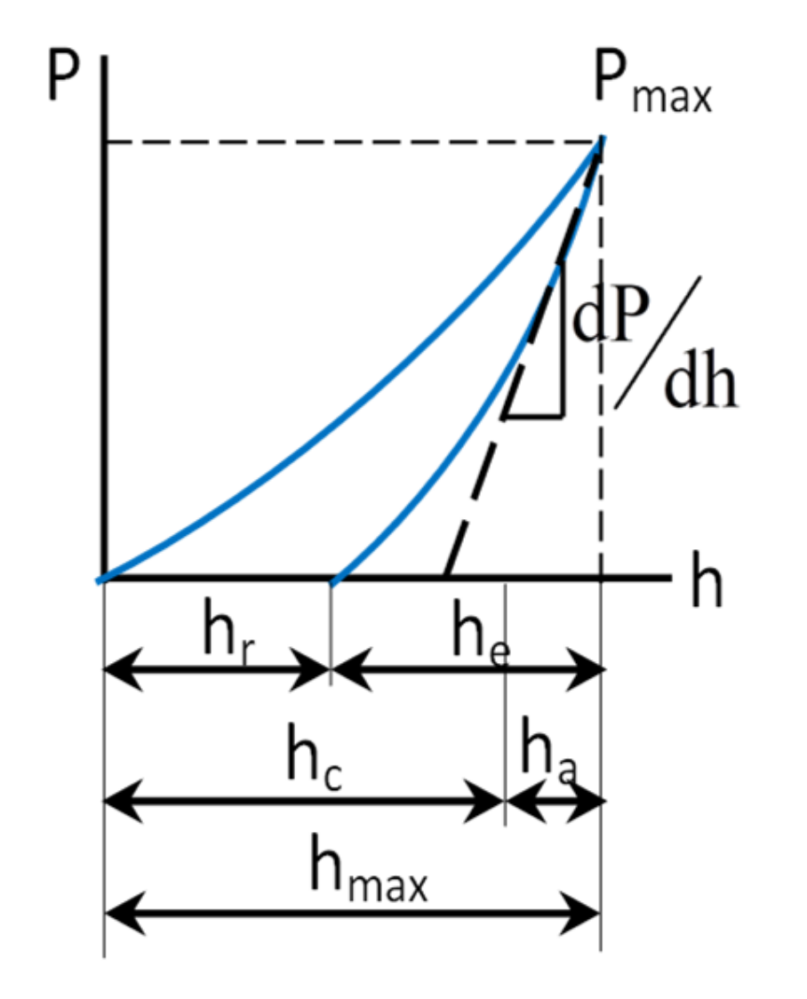
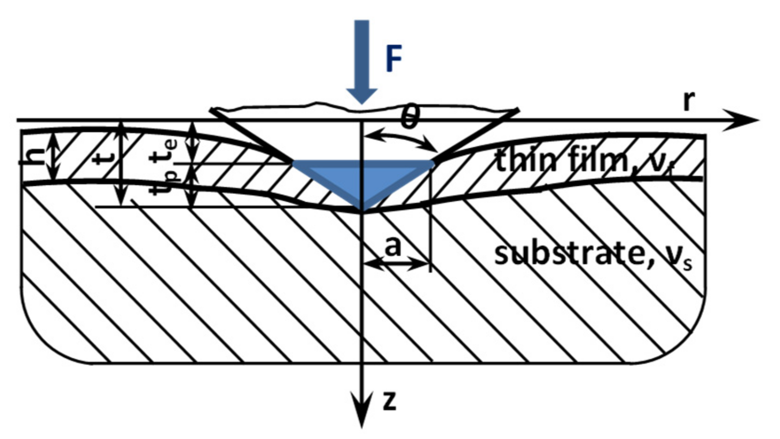
2.3. Nanoindentation
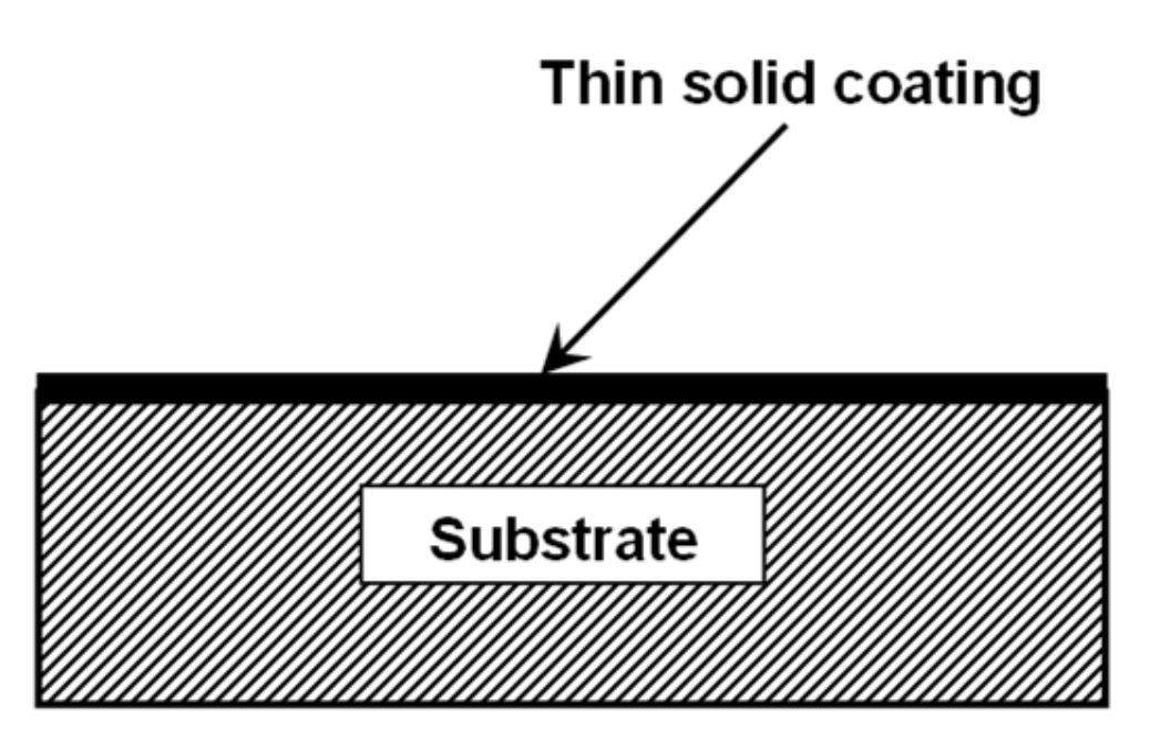
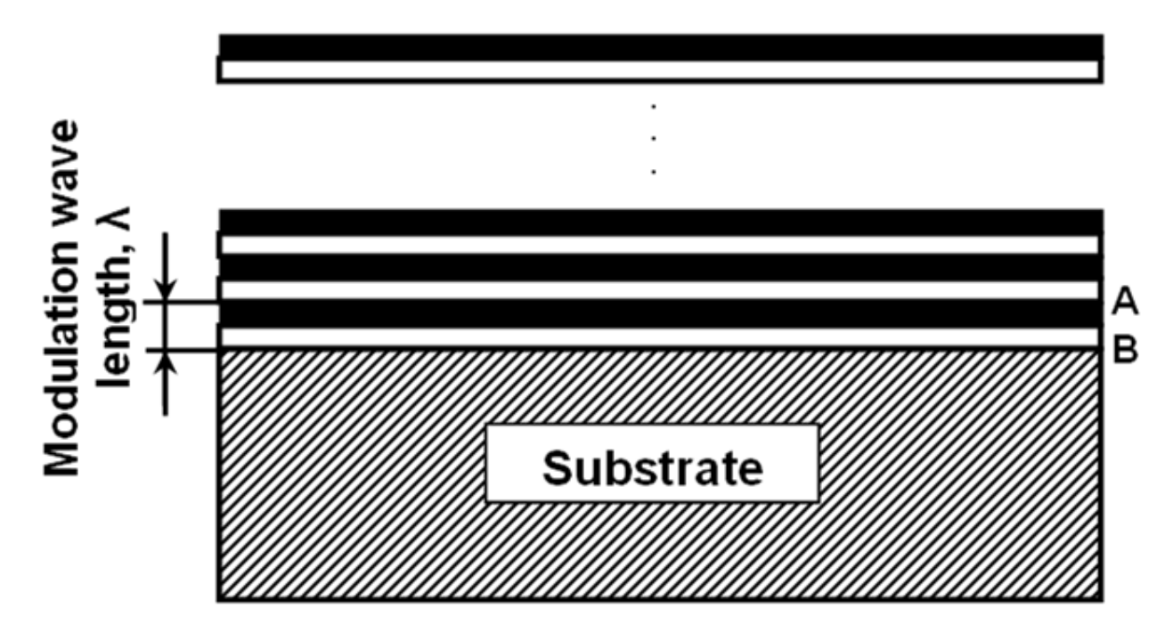
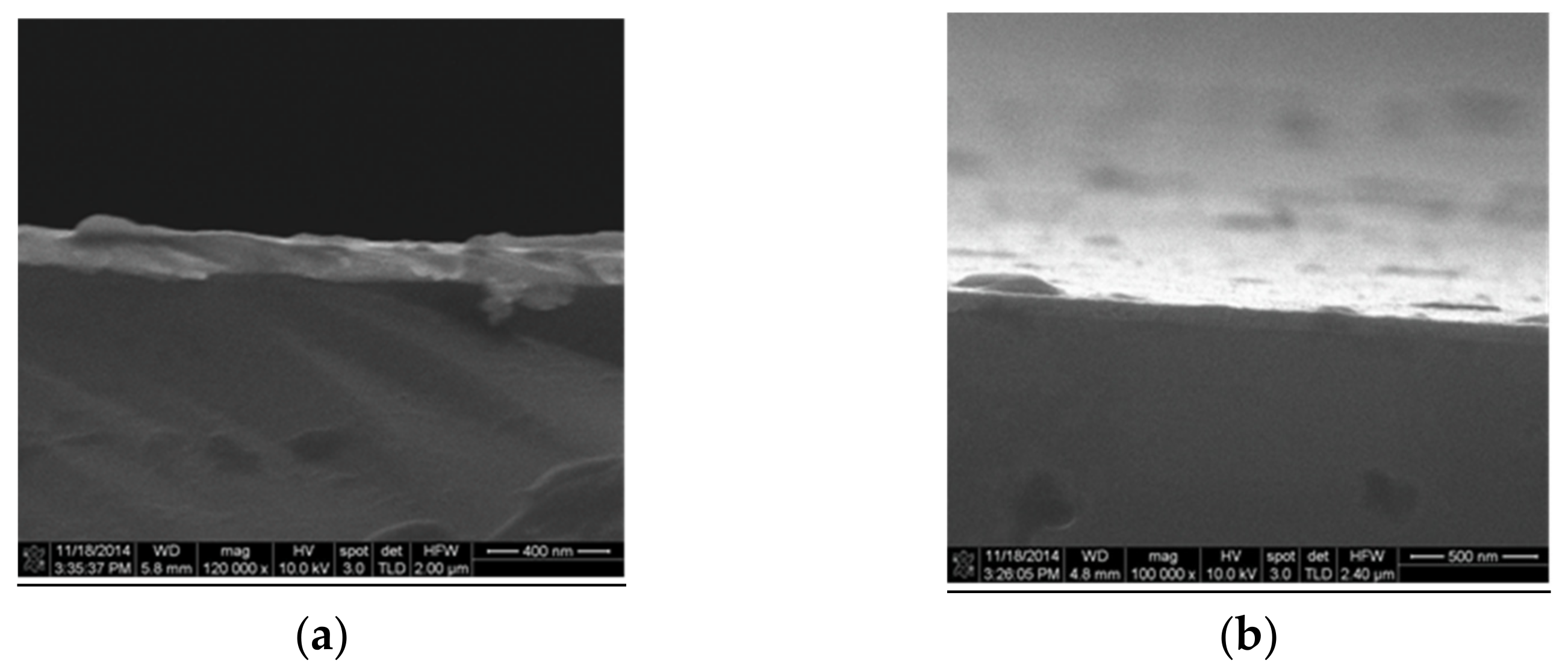
3. Thin Films for MEMS
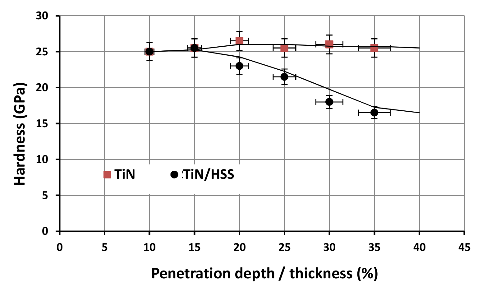
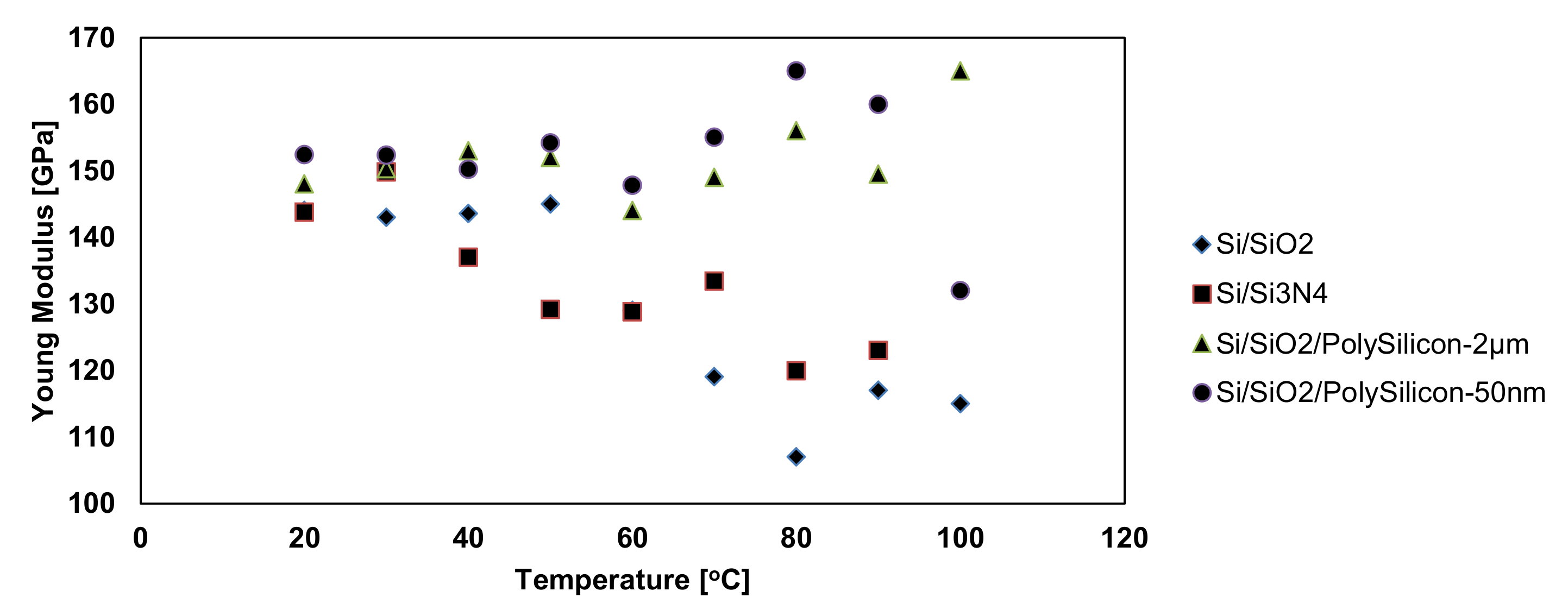
4. Thin Film Nano-Mechanical Properties
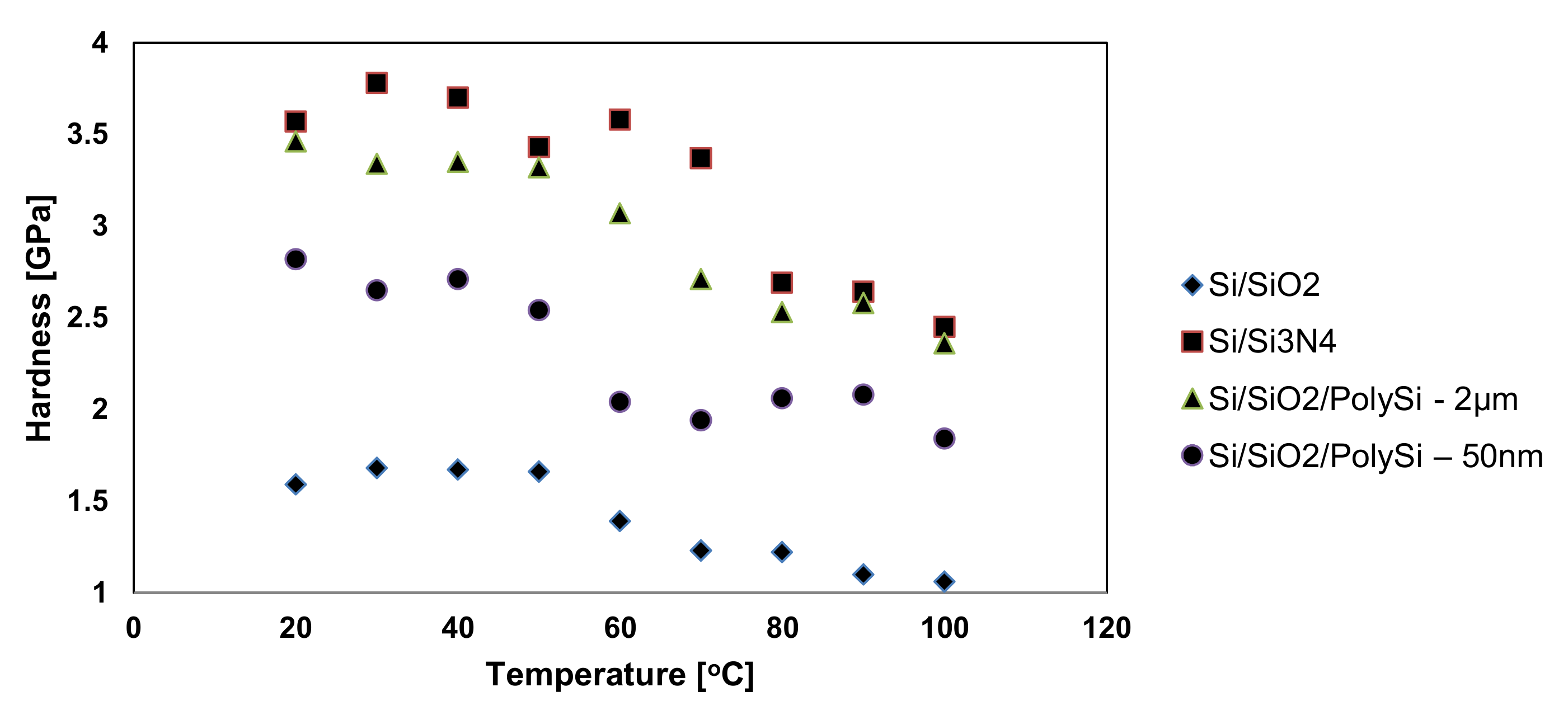
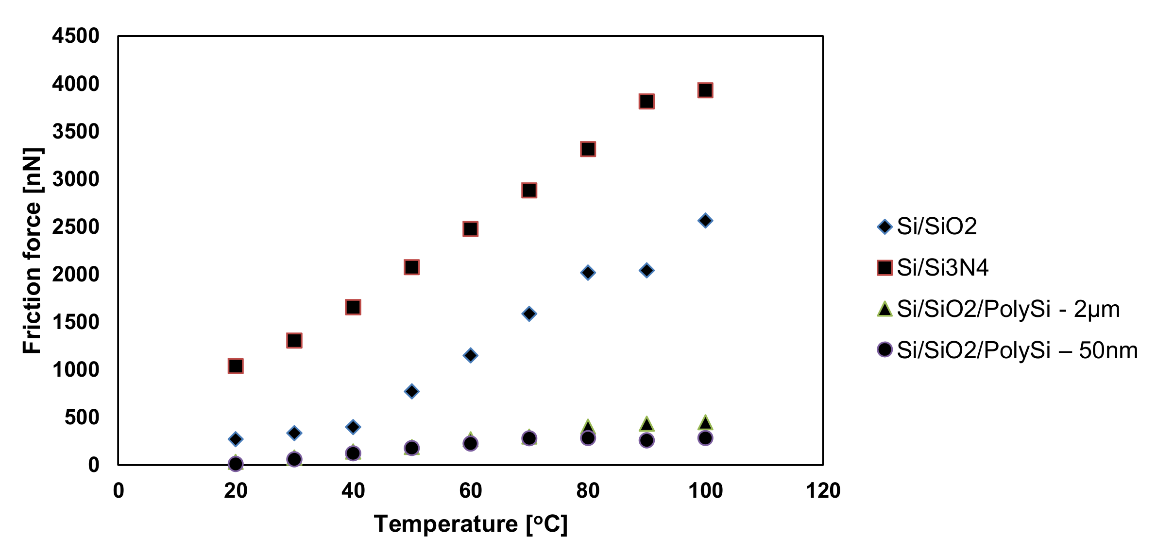
5. Thin Film Nanotribological Properties
5.1. Friction Coefficient (CoF)
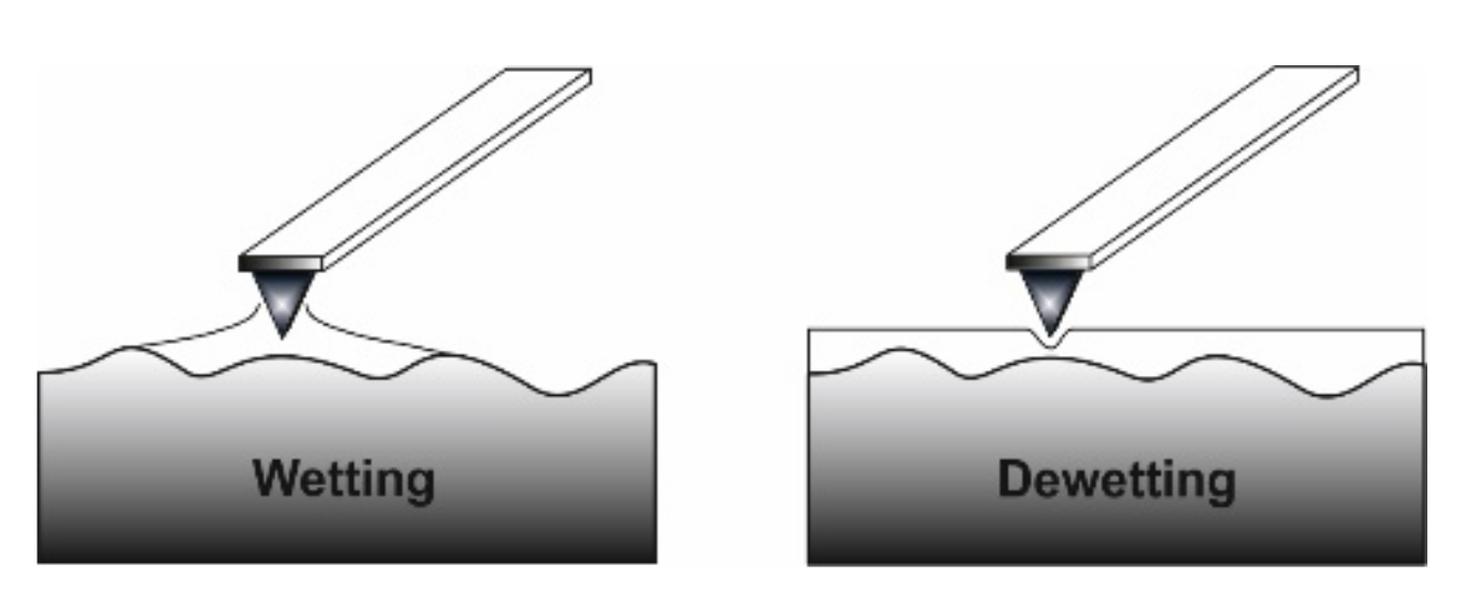
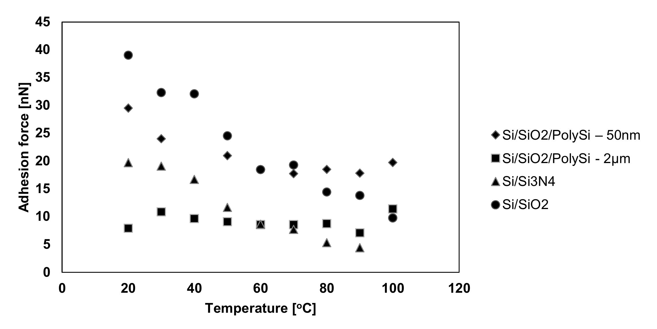
5.2. Adhesion
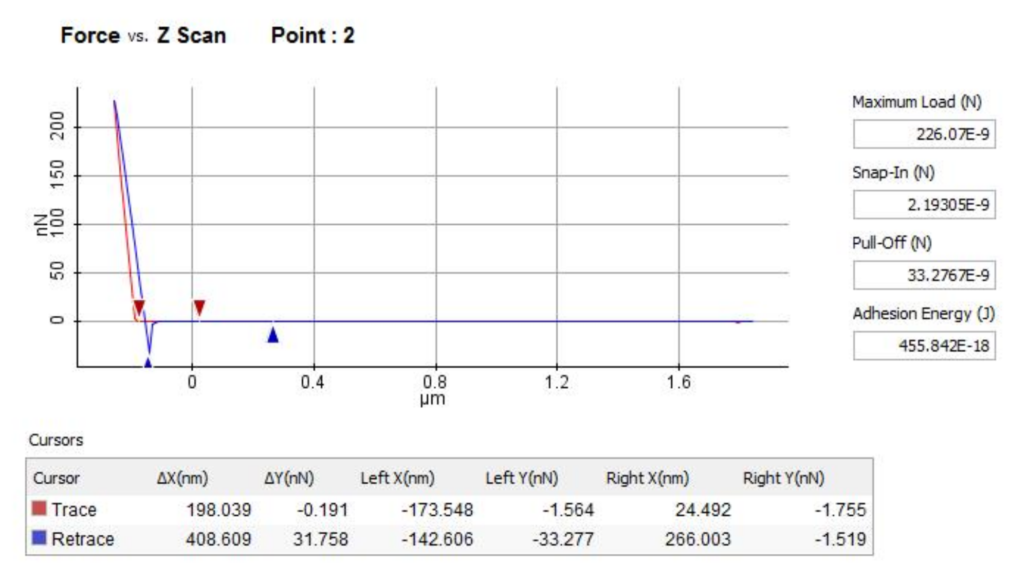
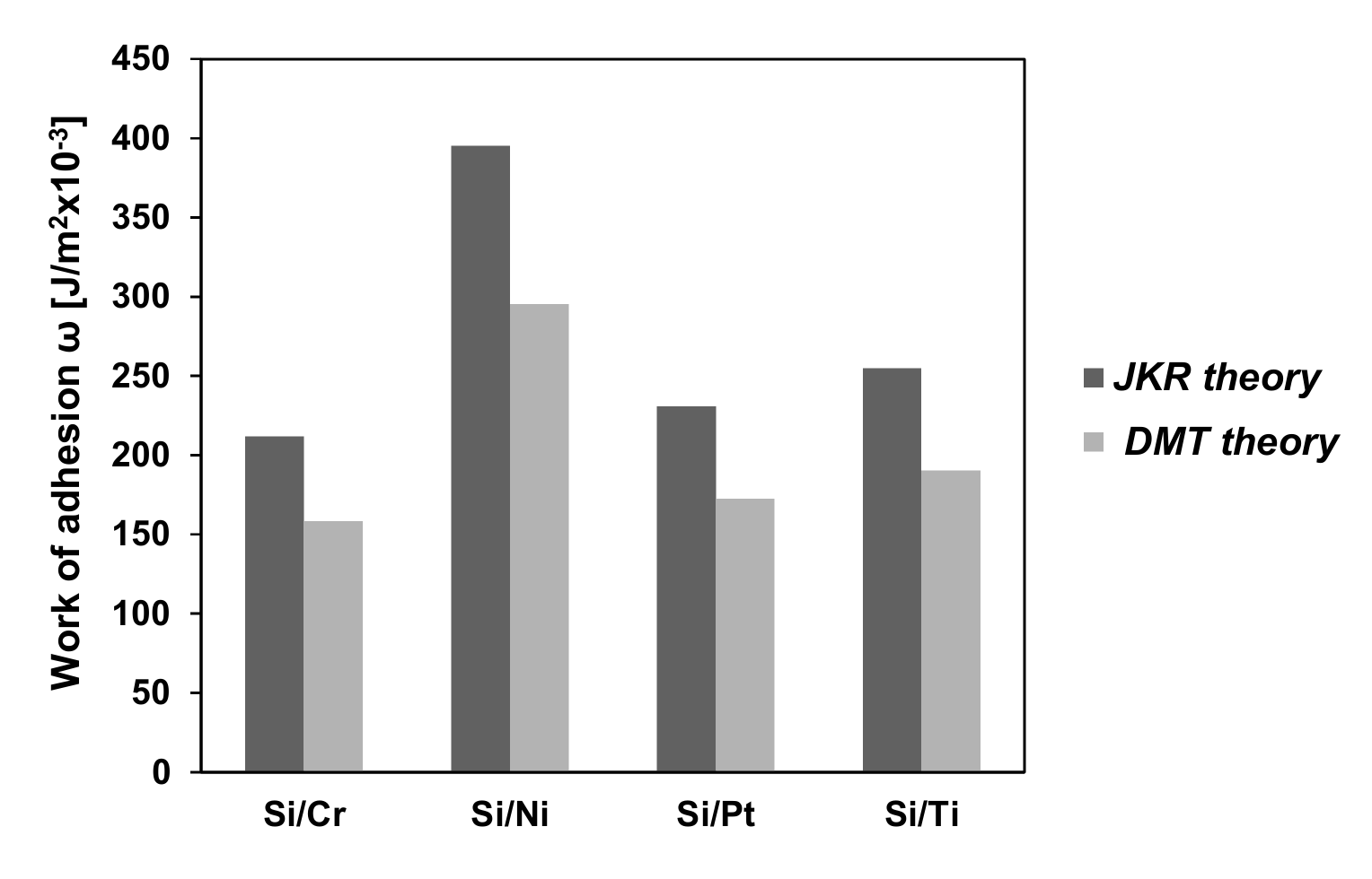
5.2.1. Single Asperity Contact
5.2.2. Multi Asperity Contact: The Greenwood and Williamson Model
6. Conclusions
Author Contributions
Funding
Conflicts of Interest
References
- Cao, X.; Jie, Y.; Wang, N.; Wang, Z.L. Triboelectric Nanogenerators Driven Self-Powered Electrochemical Processes for Energy and Environmental Science. Adv. Energy Mater. 2016, 6, 1600665. [Google Scholar] [CrossRef]
- Tambe, N.S. Nanotribological investigations of materials, coatings and lubricants for nanotechnology applications at high sliding velocities. Ph.D. Thesis, The Ohio State University, Columbus, OH, USA, 2005. [Google Scholar]
- Bhushan, B. Physical and E. Sciences, Nanotribology, nanomechanics and nanomaterials characterization. Philos. Trans. A Math. Phys. Eng. Sci. 2008, 366, 1351–1381. [Google Scholar] [PubMed]
- Li, X.; Bhushan, B.; Takashima, K.; Baek, C.-W.; Kim, Y.-K. Mechanical characterization of micro/nanoscale structures for MEMS/NEMS applications using nanoindentation techniques. Ultramicroscopy 2003, 97, 481–494. [Google Scholar] [CrossRef]
- Bhushan, B. Modern Tribology Handbook, Two Volume Set; CRC Press: Boca Raton, FL, USA, 2000. [Google Scholar]
- Maboudian, R. Critical Review: Adhesion in surface micromechanical structures. J. Vac. Sci. Technol. B Microelectron. Nanometer Struct. 1997, 15, 1–20. [Google Scholar] [CrossRef]
- Song, Y.; Nair, R.P.; Zou, M.; Wang, Y. Adhesion and friction properties of micro/nano-engineered superhydrophobic/hydrophobic surfaces. Thin Solid Film. 2010, 518, 3801–3807. [Google Scholar] [CrossRef]
- Nalwa, H.S. Handbook of Thin Films, Five-Volume Set; Elsevier: Amsterdam, The Netherlands, 2001; Volume 5. [Google Scholar]
- Bharat, B.J.B. Handbook of Micro/Nano Tribology; CRC Press: Boca Raton, FL, USA, 1999. [Google Scholar]
- Voicu, R.-C.; Pustan, M.; Birleanu, C.; Baracu, A.; Müller, R. Mechanical and tribological properties of thin films under changes of temperature conditions. Surf. Coat. Technol. 2015, 271, 48–56. [Google Scholar] [CrossRef]
- Mehrpouya, M.; Bidsorkhi, H.C. MEMS Applications of NiTi Based Shape Memory Alloys: A Review. Micro. Nanosyst. 2017, 8, 79–91. [Google Scholar] [CrossRef]
- Birleanu, C.; Pustan, M.; Merie, V.; Müller, R.; Voicu, R.; Baracu, A.; Craciun, S. Temperature effect on the mechanical properties of gold nano films with different thickness. IOP Conf. Ser. Mater. Sci. Eng. 2016, 147, 012021. [Google Scholar] [CrossRef] [Green Version]
- Hsu, S.M. Nanolubrication: Concept and Design. In Nanotribology; Springer: Boston, MA, USA, 2003; pp. 327–346. [Google Scholar] [CrossRef]
- Kumar, A.; Yadav, R.; Janyani, V.; Prasad, M. Structural study of aluminium nitride thin film grown by radio frequency sputtering technique. In Proceedings of the International Conference on Computer, Communications and Electronics COMPTELIX, Jaipur, India, 1–2 July 2017; pp. 532–535. [Google Scholar] [CrossRef]
- Gill, J.J.; Chang, D.T.; Momoda, L.A.; Carman, G.P. Manufacturing issues of thin film NiTi microwrapper. Sens. Actuators A Phys. 2001, 93, 148–156. [Google Scholar] [CrossRef]
- Fu, Y.; Du, H.; Huang, W.; Zhang, S.; Hu, M. TiNi-based thin films in MEMS applications: A review. Sens. Actuators A Phys. 2004, 112, 395–408. [Google Scholar] [CrossRef]
- Freund, L.B.; Suresh, S. Thin Film Materials: Stress, Defect Formation And Surface Evolution; Cambridge University Press: Cambridge, UK, 2004. [Google Scholar]
- Cozma, S.; Vlǎdoiu, R.; Mandes, A.; Dinca, V.; Prodan, G.; Buršíková, V. Characterization of Platinum-Based Thin Films Deposited by Thermionic Vacuum Arc (TVA) Method. Materials 2020, 13, 1796. [Google Scholar] [CrossRef]
- Kumar, P.; Bansal, D.; Anuroop; Mehta, K.; Kumar, A.; Rangra, K.; Boolchandani, D. Optimization of Titanium Nitride Film for High Power RF MEMS Applications. J. Electron. Mater. 2019, 48, 6431–6436. [Google Scholar] [CrossRef]
- TrueDyne. MEMS Technology. Available online: https://www.truedyne.com/density-measurement-basics-part-3/?lang=en,Last (accessed on 13 December 2021).
- Sharma, N.; Hooda, M.; Sharma, S.K. Synthesis and characterization of LPCVD polysilicon and silicon nitride thin films for MEMS applications. J. Mater. 2014, 2014, 1–8. [Google Scholar] [CrossRef] [Green Version]
- Guo, Y.-B.; Wang, D.-G.; Zhang, S.-W. Adhesion and friction of nanoparticles/polyelectrolyte multilayer films by AFM and micro-tribometer. Tribol. Int. 2011, 44, 906–915. [Google Scholar] [CrossRef]
- Zheng, X.; Zhou, Y. Investigation of an anisotropic plate model to evaluate the interface adhesion of thin film with cross-sectional nanoindentation method. Compos. Sci. Technol. 2005, 65, 1382–1390. [Google Scholar] [CrossRef]
- Tan, C.W.; Miao, J. Optimization of sputtered Cr/Au thin film for diaphragm-based MEMS applications. Thin Solid Film. 2009, 517, 4921–4925. [Google Scholar] [CrossRef]
- Harrison, J.; Schall, J.D.; Knippenberg, M.T.; Gao, G.; Mikulski, P.T. Elucidating atomic-scale friction using molecular dynamics and specialized analysis techniques. J. Phys. Condens. Matter 2008, 20. [Google Scholar] [CrossRef] [Green Version]
- Yoon, E.-S.; Singh, R.A.; Oh, H.-J.; Kong, H. The effect of contact area on nano/micro-scale friction. Wear 2005, 259, 1424–1431. [Google Scholar] [CrossRef]
- Dedkov, G. Theory of the noncontact friction forces between sliding nanoasperity and a surface. Wear 1999, 232, 145–150. [Google Scholar] [CrossRef]
- Ling, Z.; Qian, L.; Cheng, G.; Zhang, Z.; Sun, D. Computer Simulation of Interactions between Copper and Aluminum Nano-films. Int. J. Sci. Eng. Comput. Technol. 2013, 3, 80. [Google Scholar]
- Iizuka, T.; Onoda, A.; Hoshide, T. MD Simulation of Hardness Property of Al Thin Film Sputtered on Si Substrate and Its Related to Porosity. JSME Int. J. Ser. A 2001, 44, 346–353. [Google Scholar] [CrossRef] [Green Version]
- Xiang, W.; Zhao, C.; Liu, K.; Zhang, G.; Zhao, K. Heteroepitaxial growth of TiN thin films on Si substrates for MEMS applications. J. Alloy. Compd. 2015, 658, 862–866. [Google Scholar] [CrossRef]
- Gupta, N.; Dutta, S.; Pandey, A.; Vanjari, S.R.K.; Kaur, D. Effect of growth and residual stress in AlN (0002) thin films on MEMS accelerometer design. J. Mater. Sci. Mater. Electron. 2020, 31, 17281–17290. [Google Scholar] [CrossRef]
- Conde, J.P.; Gaspar, J.; Chu, V. Low-temperature thin-film silicon MEMS. Thin Solid Film. 2003, 427, 181–186. [Google Scholar] [CrossRef]
- Tsuchiya, T.; Tabata, O. Reliability of MEMS; Wiley-VCH: Hoboken, NJ, USA, 2008. [Google Scholar]
- Stanimirović, Z.; Stanimirovic, I. Mechanical Properties of MEMS Materials, Micro Electronic and Mechanical Systems; Takahata, K., Ed.; IntechOpen: London, UK, 2009. [Google Scholar]
- Bellitto, V. Atomic Force Microscopy: Imaging, Measuring and Manipulating Surfaces at The Atomic Scale. In Atomic Force Microscopy; IntechOpen: London, UK, 2012. [Google Scholar]
- Binnig, G.; Quate, C.F.; Gerber, C.J. Atomic force microscope. Phys. Rev. Lett. 1986, 56, 930. [Google Scholar] [CrossRef] [Green Version]
- Raczkowska, J.; Montenegro, R.; Budkowski, A.; Landfester, K.; Bernasik, A.; Rysz, J.; Czuba, P. Structure Evolution in Layers of Polymer Blend Nanoparticles. Langmuir 2007, 23, 7235–7240. [Google Scholar] [CrossRef] [PubMed]
- Munz, M.J. Force calibration in lateral force microscopy: A review of the experimental methods. J. Phys. D Appl. Phys. 2010, 43, 063001. [Google Scholar] [CrossRef]
- Bhushan, B.; Kasai, T.; Kulik, G.; Barbieri, L.; Hoffmann, P. AFM study of perfluoroalkylsilane and alkylsilane self-assembled monolayers for anti-stiction in MEMS/NEMS. Ultramicroscopy 2005, 105, 176–188. [Google Scholar] [CrossRef]
- Papastavrou, G.; Akari, S. Specific detection of interactions between uncharged surfaces in different solvents: High-resolution imaging by chemical force microscopy*. Nanotechnology 1999, 10, 453–457. [Google Scholar] [CrossRef]
- Kim, S.-K.; Jung, M.-H.; Kim, H.-W.; Woo, S.-G.; Lee, H. Measurement of the strength of adhesion of resist patterns using an atomic force microscope. Nanotechnology 2005, 16, 2227–2232. [Google Scholar] [CrossRef]
- Bowden, F.P.; Tabor, D. The Friction and Lubrication of Solids-Part II; University Press: Oxford, UK, 1964. [Google Scholar]
- Schuh, C.A. Nanoindentation studies of materials. Mater. Today 2006, 9, 32–40. [Google Scholar] [CrossRef]
- Kathalingam, A.; Marimuthu, K.P.; Karuppasamy, K.; Chae, Y.-S.; Lee, H.; Park, H.-C.; Kim, H.-S. Structural and Mechanical Characterization of Platinum Thin Films Prepared Electrochemically on ITO/Glass Substrate. Met. Mater. Int. 2019, 27, 1554–1564. [Google Scholar] [CrossRef]
- Oliver, C.W.; Pharr, G.M.J. Measurement of hardness and elastic modulus by instrumented indentation: Advances in understanding and refinements to methodology. J. Mater. Res. 2004, 19, 3–20. [Google Scholar] [CrossRef]
- Ma, D.D.D.; Lee, C.S.; Au, F.C.K.; Tong, S.Y.; Lee, S.T. Small-Diameter Silicon Nanowire Surfaces. Science 2003, 299, 1874–1877. [Google Scholar] [CrossRef]
- Fischer-Cripps, A. A simple phenomenological approach to nanoindentation creep. Mater. Sci. Eng. A 2004, 385, 74–82. [Google Scholar] [CrossRef]
- Oyen, M.L.; Cook, R.F. Load–displacement behavior during sharp indentation of viscous–elastic–plastic materials. J. Mater. Res. 2003, 18, 139–150. [Google Scholar] [CrossRef]
- Storåkers, B.; Larsson, P.-L. On Brinell and Boussinesq indentation of creeping solids. J. Mech. Phys. Solids 1994, 42, 307–332. [Google Scholar] [CrossRef]
- Swadener, J.G.; Taljat, B.; Pharr, G. Measurement of residual stress by load and depth sensing indentation with spherical indenters. J. Mater. Res. 2001, 16, 2091–2102. [Google Scholar] [CrossRef]
- Layton, A.R.; Adams, T.M. Introductory MEMS: Fabrication and Applications; Springer: Berlin/Heidelberg, Germany, 2010. [Google Scholar]
- Cheng, Y.-T.; Cheng, C. Reports, Scaling, dimensional analysis, and indentation measurements. Mater. Sci. Eng. 2004, 44, 91–149. [Google Scholar] [CrossRef]
- Fischer-Cripps, A.C. Contact Mechanics, in Nanoindentation; Springer: Berlin/Heidelberg, Germany, 2011; pp. 1–19. [Google Scholar]
- VanLandingham, M.R. Review of instrumented indentation. J. Res. Natl. Inst. Stand. Technol. 2003, 108, 249–265. [Google Scholar] [CrossRef]
- Lichinchi, M.; Lenardi, C.; Haupt, J.; Vitali, R. Simulation of Berkovich nanoindentation experiments on thin films using finite element method. Thin Solid Film. 1998, 312, 240–248. [Google Scholar] [CrossRef] [Green Version]
- Jung, Y.-G.; Lawn, B.R.; Martyniuk, M.; Huang, H.; Hu, X.Z. Evaluation of elastic modulus and hardness of thin films by nanoindentation. J. Mater. Res. 2004, 19, 3076–3080. [Google Scholar] [CrossRef]
- Chen, S.; Liu, L.; Wang, T. Investigation of the mechanical properties of thin films by nanoindentation, considering the effects of thickness and different coating–substrate combinations. Surf. Coat. Technol. 2005, 191, 25–32. [Google Scholar] [CrossRef]
- Reusch, M.; Cherneva, S.; Lu, Y.; Žukauskaitė, A.; Kirste, L.; Holc, K.; Datcheva, M.; Stoychev, D.; Lebedev, V.; Ambacher, O. Microstructure and mechanical properties of stress-tailored piezoelectric AlN thin films for electro-acoustic devices. Appl. Surf. Sci. 2017, 407, 307–314. [Google Scholar] [CrossRef]
- Chauhan, S.S.; Manhas, S.K.; Joglekar, M. Fabrication of cantilever MEMs structure of C-axis grown AlN film for energy harvester application. In Proceedings of the 2018 IEEE International Conference on Industrial Technology (ICIT), Lyon, France, 20–22 February 2018. [Google Scholar]
- Volinsky, A.A.; Moody, N.R.; Gerberich, W.W. Nanoindentation of Au and Pt/Cu thin films at elevated temperatures. J. Mater. Res. 2004, 19, 2650–2657. [Google Scholar] [CrossRef] [Green Version]
- Verdyan, A. Nano indentation inspection of the mechanical properties of gold nitride thin films. In Proceedings of the 3rd International Conference on Cybernetics and Information Technologies, Systems, and Applicat/4th International Conference on Computing, Communications and Control Technologies, Berkeley, CA, USA, 25–26 May 2006. [Google Scholar]
- Soh, M.T.K.; Fischer-Cripps, A.C.; Savvides, N. Elastic modulus of silicon nitride thin films from nanoindentation. In Proceedings of the 16th National Congress of the Australian Institute of Physics, Congress Proceedings Handbook and Abstracts, Canberra, Australia, 30 January–4 February 2005. [Google Scholar]
- Cao, Y.; Allameh, S.; Nankivil, D.; Sethiaraj, S.; Otiti, T.; Soboyejo, W. Nanoindentation measurements of the mechanical properties of polycrystalline Au and Ag thin films on silicon substrates: Effects of grain size and film thickness. Mater. Sci. Eng. A 2006, 427, 232–240. [Google Scholar] [CrossRef]
- Sundararajan, S.; Bhushan, B. Micro/nanotribological studies of polysilicon and SiC films for MEMS applications. Wear 1998, 217, 251–261. [Google Scholar] [CrossRef]
- Li, X.; Bhushan, B. Micro/nanomechanical characterization of ceramic films for microdevices. Thin Solid Film. 1999, 340, 210–217. [Google Scholar] [CrossRef]
- Luo, J.; Hu, Y.; Wen, S. Physics and Chemistry of Micro-nanotribology; ASTM International: West Conshohocken, PA, USA, 2008. [Google Scholar]
- Sarkar, L.; Singh, S.G.; Vanjari, S.R.K. Preparation and optimization of PVDF thin films for miniaturized sensor and actuator applications. Smart Mater. Struct. 2021, 30, 075013. [Google Scholar] [CrossRef]
- Koehler, J.S. Attempt to Design a Strong Solid. Phys. Rev. B 1970, 2, 547–551. [Google Scholar] [CrossRef]
- Lehoczky, S.L. Strength enhancement in thin-layered Al-Cu laminates. J. Appl. Phys. 1978, 49, 5479. [Google Scholar] [CrossRef]
- Ruud, J.A.; Jervis, T.R.; Spaepen, F. Nanoindentation of Ag/Ni multilayered thin films. J. Appl. Phys. 1994, 75, 4969–4974. [Google Scholar] [CrossRef] [Green Version]
- Choi, Y.; Van Vliet, K.J.; Li, J.; Suresh, S. Size effects on the onset of plastic deformation during nanoindentation of thin films and patterned lines. J. Appl. Phys. 2003, 94, 6050–6058. [Google Scholar] [CrossRef]
- Son, D.; Jeong, J.-H.; Kwon, D. Film-thickness considerations in microcantilever-beam test in measuring mechanical properties of metal thin film. Thin Solid Film. 2003, 437, 182–187. [Google Scholar] [CrossRef]
- Guo, J.-G.; Zhao, Y.-P. The size-dependent elastic properties of nanofilms with surface effects. J. Appl. Phys. 2005, 98, 74306. [Google Scholar] [CrossRef] [Green Version]
- Krivtsov, A.M.; Morozov, N.F. On mechanical characteristics of nanocrystals. Phys. Solid State 2002, 44, 2260–2265. [Google Scholar] [CrossRef]
- Yang, F.J.J. Size-dependent effective modulus of elastic composite materials: Spherical nanocavities at dilute concentrations. J. Appl. Phys. 2004, 95, 3516–3520. [Google Scholar] [CrossRef]
- Streitz, H.F.; Cammarata, R.C.; Sieradzki, K. Surface-stress effects on elastic properties. I. Thin metal films. Phys. Rev. B 1994, 49, 10699. [Google Scholar] [CrossRef]
- Zhang, H.; Sun, C.T. Nanoplate Model for Platelike Nanomaterials. AIAA J. 2004, 42, 2002–2009. [Google Scholar] [CrossRef]
- Workum, V.; de Pablo, J. Local elastic constants in thin films of an fcc crystal. Phys. Rev. 2003, 67, 031601. [Google Scholar] [CrossRef] [Green Version]
- Nan, C.; Li, X.; Cai, K.; Tong, J. Grain Size-dependent Elastic Moduli of Nanocrystals. J. Mater. Sci. Lett. 1998, 17, 1917–1919. [Google Scholar] [CrossRef]
- Sharma, P.; Ganti, S. On the grain-size-dependent elastic modulus of nanocrystalline materials with and without grain-boundary sliding. J. Mater. Res. 2003, 18, 1823–1826. [Google Scholar] [CrossRef]
- Villain, P.; Beauchamp, P.; Badawi, K.; Goudeau, P.; Renault, P.-O. Atomistic calculation of size effects on elastic coefficients in nanometre-sized tungsten layers and wires. Scr. Mater. 2004, 50, 1247–1251. [Google Scholar] [CrossRef]
- Broughton, J.Q.; Meli, C.A.; Vashishta, P.; Kalia, R.K. Direct atomistic simulation of quartz crystal oscillators: Bulk properties and nanoscale devices. Phys. Rev. B 1997, 56, 611–618. [Google Scholar] [CrossRef]
- Miller, R.; Shenoy, V.B. Size-dependent elastic properties of nanosized structural elements. Nanotechnology 2000, 11, 139–147. [Google Scholar] [CrossRef]
- Fedorchenko, A.I.; Wang, A.-B.; Cheng, H.H. Thickness dependence of nanofilm elastic modulus. Appl. Phys. Lett. 2009, 94, 152111. [Google Scholar] [CrossRef]
- Luo, J. Young’s modulus of electroplated Ni thin film for MEMS applications. Mater. Lett. 2004, 58, 2306–2309. [Google Scholar] [CrossRef]
- Chinmulgund, M.; Inturi, R.; Barnard, J. Effect of Ar gas pressure on growth, structure, and mechanical properties of sputtered Ti, Al, TiAl, and Ti3Al films. Thin Solid Film. 1995, 270, 260–263. [Google Scholar] [CrossRef]
- Keller, R.-M.; Baker, S.P.; Arzt, E. Quantitative analysis of strengthening mechanisms in thin Cu films: Effects of film thickness, grain size, and passivation. J. Mater. Res. 1998, 13, 1307–1317. [Google Scholar] [CrossRef]
- Arzt, E.J. Size effects in materials due to microstructural and dimensional constraints: A comparative review. Acta Mater. 1998, 46, 5611–5626. [Google Scholar] [CrossRef] [Green Version]
- Kraft, O.; Schwaiger, R.; Wellner, P. Fatigue in thin films: Lifetime and damage formation. Mater. Sci. Eng. A 2001, 319–321, 919–923. [Google Scholar] [CrossRef]
- Ogawa, H.; Suzuki, K.; Kaneko, S.; Nakano, Y.; Ishikawa, Y.; Kitahara, T. Tensile testing of microfabricated thin films. Microsyst. Technol. 1997, 3, 117–121. [Google Scholar] [CrossRef]
- Tsuchiya, T.; Hirata, M.; Chiba, N. Young’s modulus, fracture strain, and tensile strength of sputtered titanium thin films. Thin Solid Film. 2005, 484, 245–250. [Google Scholar] [CrossRef]
- Tall, P.D.; Ndiaye, S.; Beye, A.C.; Zong, Z.; Soboyejo, W.O.; Lee, H.-J.; Ramirez, A.G.; Rajan, K. Nanoindentation of Ni–Ti thin films. Mater. Manuf. Process. 2007, 22, 175–179. [Google Scholar] [CrossRef]
- Hay, J.L.; O’Hern, M.E.; Oliver, W.C. Tie Importance of Contact Radius for Substrate-Independent Property Measurement of Thin Films. MRS Proc. 1998, 522. [Google Scholar] [CrossRef]
- Huajian, G.; Cheng-Hsin, C.; Jin, L. Elastic contact versus indentation modeling of multi-layered materials. Int. J. Solids Struct. 1992, 29, 2471–2492. [Google Scholar] [CrossRef]
- Puchi-Cabrera, E.J.S. Technology, A new model for the computation of the composite hardness of coated systems. Surf. Coat. Technol. 2002, 160, 177–186. [Google Scholar] [CrossRef]
- Birleanu, C.; Pustan, M. Size effect on stiffness and pull-off force of thermally actuated gold cantilevers. Rom. J. Tech. Sci. Appl. Mech. 2017, 62, 145–162. [Google Scholar]
- Sun, Y.; Hu, Z.; Zhao, D.; Zeng, K. Mechanical Properties of Microcrystalline Metal–Organic Frameworks (MOFs) Measured by Bimodal Amplitude Modulated-Frequency Modulated Atomic Force Microscopy. ACS Appl. Mater. Interfaces 2017, 9, 32202–32210. [Google Scholar] [CrossRef]
- Garcia, R.; Proksch, R. Nanomechanical mapping of soft matter by bimodal force microscopy. Eur. Polym. J. 2013, 49, 1897–1906. [Google Scholar] [CrossRef]
- Hayward, I.; Singer, I.; Seitzman, L. Effect of roughness on the friction of diamond on cvd diamond coatings. Wear 1992, 157, 215–227. [Google Scholar] [CrossRef]
- Leyland, A.; Matthews, A. Design criteria for wear-resistant nanostructured and glassy-metal coatings. Surf. Coat. Technol. 2004, 177–178, 317–324. [Google Scholar] [CrossRef]
- Zhao, W.; Pu, J.; Yu, Q.; Zeng, Z.; Wu, X.; Xue, Q. A Novel strategy to enhance micro/nano-tribological properties of DLC film by combining micro-pattern and thin ionic liquids film. Colloids Surf. A Physicochem. Eng. Asp. 2013, 428, 70–78. [Google Scholar] [CrossRef]
- Birleanu, C.; Pustan, M. The effect of film thickness on the tribomechanical properties of the chrome-gold thin film. In Proceedings of the 2016 Symposium on Design, Test, Integration and Packaging of MEMS/MOEMS (DTIP), Budapest, Hungary, 30 May–2 June 2016; pp. 1–6. [Google Scholar] [CrossRef]
- Merie, V.V.; Bȋrleanu, C.; Pustan, M.S.; Negrea, G.; Pintea, I.M. Analysis on temperature effect on the mechanical and tribological properties of titanium nitride thin films. IOP Conf. Ser. Mater. Sci. Eng. 2016, 147, 012019. [Google Scholar] [CrossRef]
- Lee, W.-S.; Liu, T.-Y.; Chen, T.-H. Nanoindentation Behaviour and Microstructural Evolution of Au/Cr/Si Thin Films. Mater. Trans. 2009, 50, 1768–1777. [Google Scholar] [CrossRef] [Green Version]
- Charitidis, C.A.; Koumoulos, E.P.; Dragatogiannis, D.A. Nanotribological Behavior of Carbon Based Thin Films: Friction and Lubricity Mechanisms at the Nanoscale. Lubricants 2013, 1, 22–47. [Google Scholar] [CrossRef] [Green Version]
- Tomala, A.; Roy, M.; Franek, F. Nanotribology of Mo–Se–C films. Philos. Mag. 2010, 90, 3827–3843. [Google Scholar] [CrossRef]
- Wang, J.; Sottos, N.R.; Weaver, R.L. Tensile and mixed-mode strength of a thin film-substrate interface under laser induced pulse loading. J. Mech. Phys. Solids 2004, 52, 999–1022. [Google Scholar] [CrossRef]
- Arias, D.F.; Marulanda, D.M.; Baena, A.M.; Devia, A. Determination of friction coefficient on ZrN and TiN using lateral force microscopy (LFM). Wear 2006, 261, 1232–1236. [Google Scholar] [CrossRef]
- Kumar, D.D.; Kumar, N.; Kalaiselvam, S.; Dash, S.; Jayavel, R. Micro-tribo-mechanical properties of nanocrystalline TiN thin films for small scale device applications. Tribol. Int. 2015, 88, 25–30. [Google Scholar] [CrossRef]
- Grill, A.; Patel, V. Tribological properties of diamond-like carbon and related materials. Diam. Relat. Mater. 1993, 2, 597–605. [Google Scholar] [CrossRef]
- Ipaz, L. Nanofriction study using atomic force microscopy (AFM) of multilayers based in titanium, chromium and aluminum. Strength Mater. 2012, 46, 1395–1403. [Google Scholar]
- Xie, G.; Ding, J.; Zheng, B.; Xue, W. Investigation of adhesive and frictional behavior of GeSbTe films with AFM/FFM. Tribol. Int. 2009, 42, 183–189. [Google Scholar] [CrossRef]
- Bhushan, B.; Kulkarni, A.V. Effect of normal load on microscale friction measurements. Thin Solid Films 1996, 278, 49–56. [Google Scholar] [CrossRef]
- Tambe, N.; Bhushan, B. Scale dependence of micro/nano-friction and adhesion of MEMS/NEMS materials, coatings and lubricants. Nanotechnology 2004, 15, 1561–1570. [Google Scholar] [CrossRef]
- Kumar, V.; Singhal, R. Impact of SHI on structural and mechanical behavior of intermetallic NiTi thin films. Phys. B Condens. Matter 2018, 546, 80–88. [Google Scholar] [CrossRef]
- Birleanu, C.; Merie, V.; Crisan, H.G. Effect of film thickness on the tribo-mechanical properties of chrome-gold thin films. Proceedings of the Romanian Academy Series A-Mathematics Physics Technical Sciences Information. UTPRESS 2019, 20, 174–183. [Google Scholar]
- Pustan, M.; Dudescu, C.; Birleanu, C.; Rymuza, Z. Nanomechanical studies and materials characterization of metal/polymer bilayer MEMS cantilevers. Int. J. Mater. Res. 2013, 104, 408–414. [Google Scholar] [CrossRef]
- Chau, A.; Régnier, S.; Delchambre, A.; Lambert, P. Theoretical and Experimental Study of the Influence of AFM Tip Geometry and Orientation on Capillary Force. J. Adhes. Sci. Technol. 2010, 24, 2499–2510. [Google Scholar] [CrossRef] [Green Version]
- Fuller, K.N.G.; Tabor, D. The effect of surface roughness on the adhesion of elastic solids. Proc. R. Soc. Lond. Ser. A Math. Phys. Sci. 1975, 345, 327–342. [Google Scholar] [CrossRef] [Green Version]
- Alley, R.L. Surface roughness modification of interfacial contacts in polysilicon microstructures. In Proceedings of the 7th International Conference Sensors and Actuators, Yokohama, Japan, 7–10 June 1993. [Google Scholar]
- Wong, C.H. Friction at Nanoscale. J. Appl. Mech. Eng. 2012, 01, 1–2. [Google Scholar] [CrossRef] [Green Version]
- Mishra, M.; Egberts, P.; Bennewitz, R.; Szlufarska, I. Friction model for single-asperity elastic-plastic contacts. Phys. Rev. B 2012, 86, 045452. [Google Scholar] [CrossRef] [Green Version]
- Timoshenko, S.; Goodier, J.J.I. Theory of Elasticity; McGraw-Hill Company: New York, NY, USA, 1970. [Google Scholar]
- Derjaguin, B.; Muller, V.; Toporov, Y. Effect of contact deformations on the adhesion of particles. J. Colloid Interface Sci. 1975, 53, 314–326. [Google Scholar] [CrossRef]
- Tas, N.C.; Gui, M. Elwenspoek. Static friction in elastic adhesive MEMS contacts, models and experiment. In Proceedings of the IEEE Thirteenth Annual International Conference on Micro Electro Mechanical Systems (Cat. No. 00CH36308), Miyazaki, Japan, 23–27 January 2000. [Google Scholar]
- Greenwood, J.A.; Williamson, J.B.P. Contact of nominally flat surfaces. Proc. R. Soc. Lond. Ser. A Math. Phys. Sci. 1966, 295, 300–319. [Google Scholar] [CrossRef]
- Gao, G.T.; Mikulski, P.T.; Harrison, J.A. Molecular-Scale Tribology of Amorphous Carbon Coatings: Effects of Film Thickness, Adhesion, and Long-Range Interactions. J. Am. Chem. Soc. 2002, 124, 7202–7209. [Google Scholar] [CrossRef]
- Grierson, D.S. Nanotribological properties of nanostructured hard carbon thin films. Ph.D. Thesis, The University of Wisconsin, Madison, WI, USA, 2008. [Google Scholar]
- Suresh, S.; Nieh, T.-G.; Choi, B. Nano-indentation of copper thin films on silicon substrates. Scr. Mater. 1999, 41, 951–957. [Google Scholar] [CrossRef] [Green Version]
- Guo, J.-G.; Zhou, L.-J.; Zhao, Y.-P. Size-dependent elastic modulus and fracture toughness of the nanofilm with surface effects. Surf. Rev. Lett. 2008, 15, 599–603. [Google Scholar] [CrossRef]


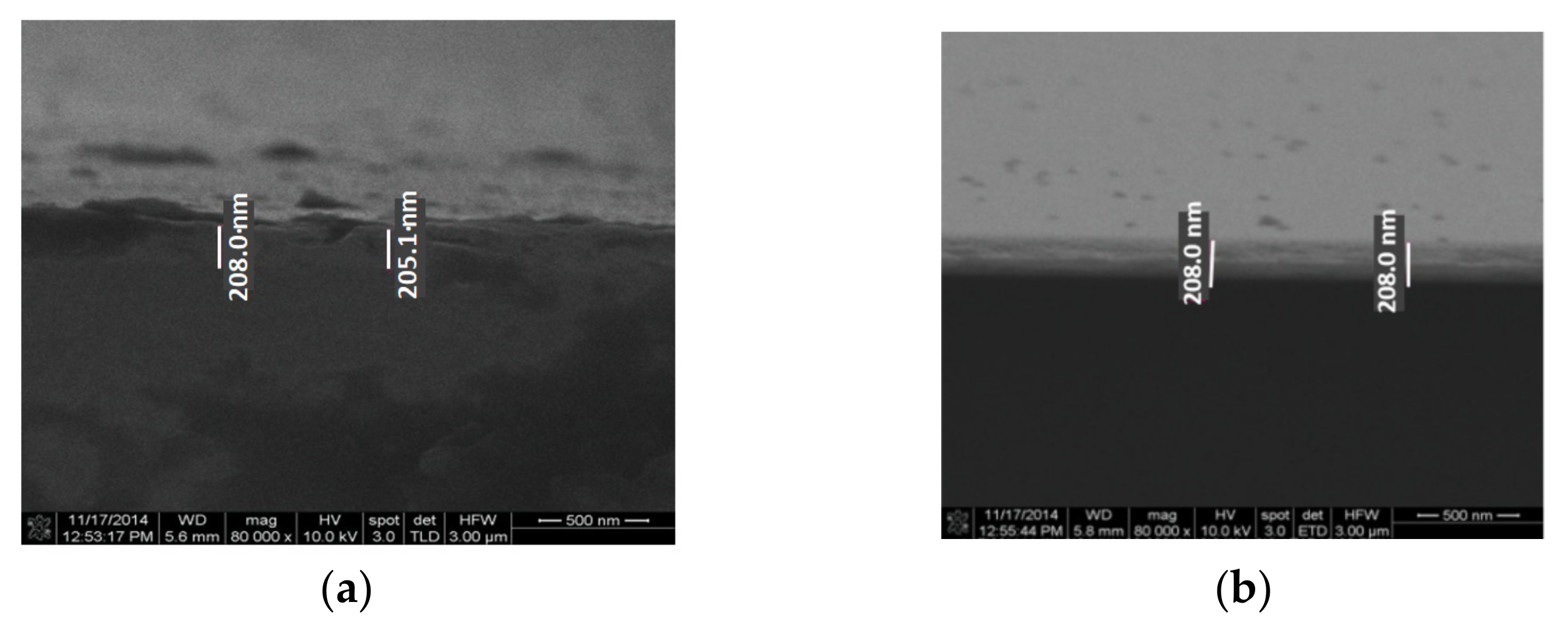
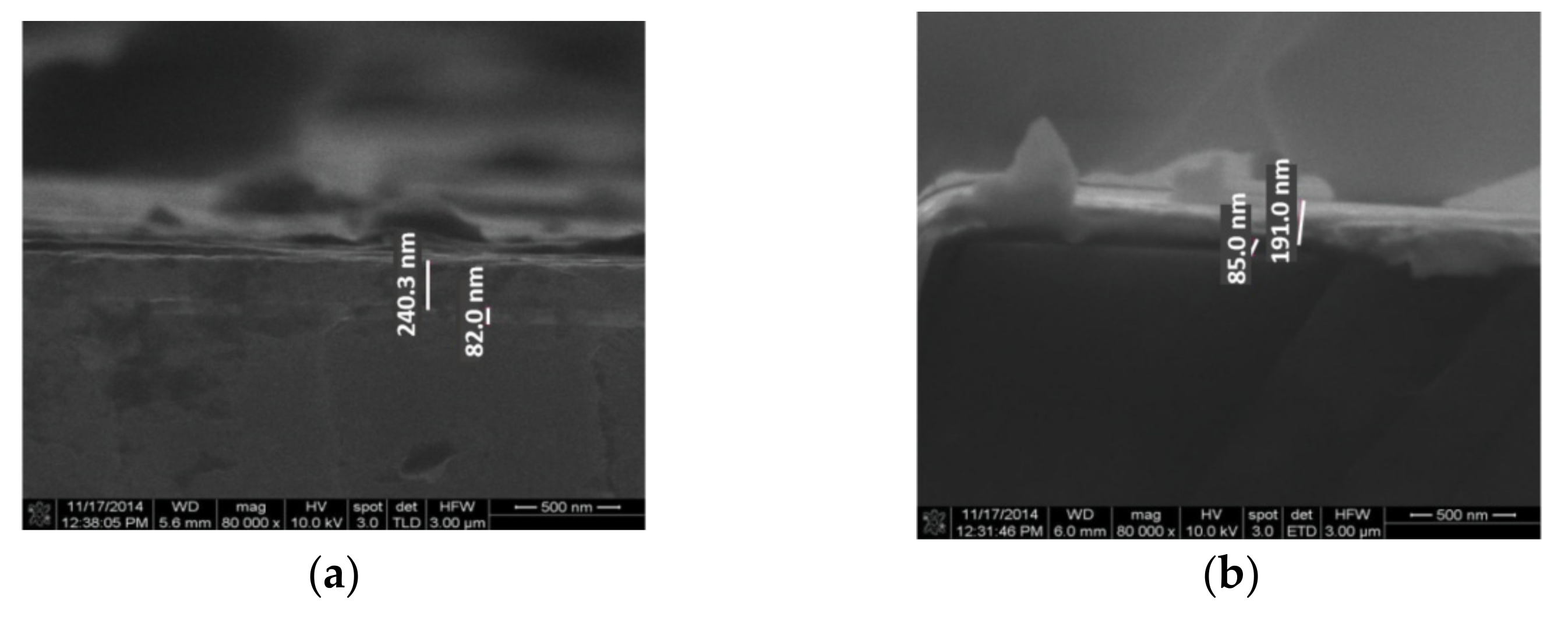
| Sample | Si/Cr | Si/Ni | Si/Pt | Si/Ti |
|---|---|---|---|---|
| Ef (GPa) | 148.9566 | 120.0840 | 104.4746 | 109.5806 |
| Hf (GPa) | 9.002–9.108 | 9.127–9.298 | 8.97–9.18 | 9.204–9.322 |
| Hf/Ef | 0.055–0.061 | 0.076–0.077 | 0.086–0.088 | 0.084–0.085 |
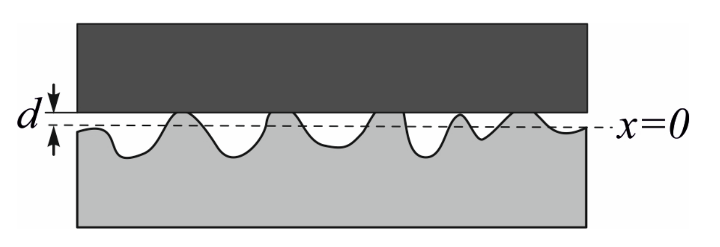
| Samples | Roughness (nm) | |||
|---|---|---|---|---|
| Ra medium | Rz medium | Rq medium | Max. Error (%) | |
| Si/Cr | 0.958 | 13.167 | 1.234 | (±4.21%) |
| Si/Ni | 0.238 | 2.848 | 0.303 | (±3.23%) |
| Si/Ti | 1.345 | 27.482 | 1.707 | (±1.36%) |
| Si/Pt | 2.097 | 21.931 | 2.659 | (±3.19%) |
| Sample | Si/Cr | Si/Ni | Si/Pt | Si/Ti |
|---|---|---|---|---|
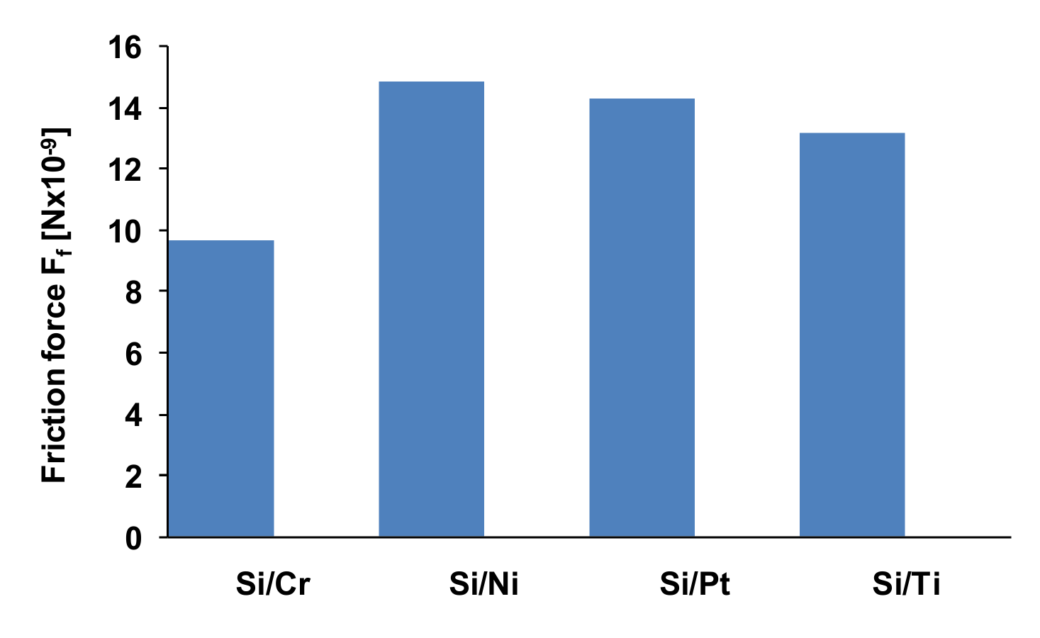
| Pull-off force medium (10−9 N) | 17.966 | 33.524 | 19.585 | 21.6303 |
| max. error (%) | (±4.438%) | (±3.858%) | (±2.758%) | (±3.878%) |
| σpull-off | 0.6524 | 0.3169 | 0.4437 | 0.839 |
Publisher’s Note: MDPI stays neutral with regard to jurisdictional claims in published maps and institutional affiliations. |
© 2021 by the authors. Licensee MDPI, Basel, Switzerland. This article is an open access article distributed under the terms and conditions of the Creative Commons Attribution (CC BY) license (https://creativecommons.org/licenses/by/4.0/).
Share and Cite
Bîrleanu, C.; Pustan, M.; Șerdean, F.; Merie, V. AFM Nanotribomechanical Characterization of Thin Films for MEMS Applications. Micromachines 2022, 13, 23. https://doi.org/10.3390/mi13010023
Bîrleanu C, Pustan M, Șerdean F, Merie V. AFM Nanotribomechanical Characterization of Thin Films for MEMS Applications. Micromachines. 2022; 13(1):23. https://doi.org/10.3390/mi13010023
Chicago/Turabian StyleBîrleanu, Corina, Marius Pustan, Florina Șerdean, and Violeta Merie. 2022. "AFM Nanotribomechanical Characterization of Thin Films for MEMS Applications" Micromachines 13, no. 1: 23. https://doi.org/10.3390/mi13010023