Article

A Mutual Capacitance Touch Readout IC with Synchronization in Touch and Mobile Display Driving for High Refresh Rate AMOLED Panels

Department of Electronic Materials Engineering, Kwangwoon University, Seoul 01897, Korea
Micromachines 2021, 12(8), 922; https://doi.org/10.3390/mi12080922
Submission received: 30 June 2021 / Revised: 28 July 2021 / Accepted: 29 July 2021 / Published: 31 July 2021
(This article belongs to the Special Issue Micro/Nanosystems for Capacitive Sensors)

Abstract

:
This paper presents a mutual capacitance touch readout IC architecture for 120 Hz high-refresh-rate AMOLED displays. In high-refresh-rate AMOLED panels, whole pixels in a horizontal line should be updated without any time-sharing with each other, leading to an amplified display noise on touch screen panel (TSP) electrodes. The proposed system architecture mitigates severe display noise by synchronizing the driving for the TSP and AMOLED pixel circuits. The proposed differential sensing technique, which is based on noise suppression in reference to mutual capacitance channels, minimizes common-mode display noise. In the front-end circuit, intrinsic circuit offset is cancelled by a chopping scheme, which correlates to the phase of the driving signals in the TSP driver and operating clocks of the front-end. Operating at a 120 Hz scan-rate, it reduces display noise by more than 11.6 dB when compared with the conventional single-ended TSP sensing method. With a built-in 130-nm CMOS, a prototype IC occupies an area of 8.02 mm2 while consuming 6.4-mW power from a 3.3 V analog voltage supply.

1. Introduction

Nowadays, with increasing demand for high-quality mobile device displays, display vendors strive to advance their technology featuring ultra-thin, transparent, and fast response time displays. Recent significant progress in mobile display driver integrated chips (MDDI) and pixel circuit technology results in the “seamless display”, or an introduction of a high refresh rate [1] in mobile devices where the MDDI updates each display frame within 8.33 milliseconds. In addition, a variable refresh rate (VRR) [2] is employed in high-end smartphones, in which the refresh rate is adjusted automatically depending on the display content. A refresh rate less than 10 Hz can be maintained for a static display image such as an always-on-display (AOD) function [3], while a fast frame transition of 120 Hz is needed for high-resolution gaming content.
Figure 1a illustrates an equivalent circuit and the stack-up of an active-matrix organic light-emitting diode (AMOLED) pixel and touch screen panel (TSP) when MDDI operates. In an on-cell display panel [4], TSP electrodes are deposited and attached onto a display pixel layer using optically clear adhesive (OCA) in a separate manufacturing process. However, in case of AMOLED panels, TSP electrodes are directly printed over the encapsulation glass which protects AMOLED pixel from oxidation and physical damage. Therefore, the ground plane for AMOLED pixel should be shared with TSP readout system. Active shielding in the ground plane [4,5] cannot be applied to AMOLED display systems, which is more vulnerable to display noise and the effects of TSP parasitic capacitance.
The MDDI, consisting of a binary amplifier (B-Amp) and a resistive digital-to-analog converter (R-DAC), provides RGB signals, and the thin-film transistor circuit in the AMOLED receives and updates these signals into the array of pixels (P[H:1]). Demultiplexers (Demux) at the MDDI output have been widely adopted for low-resolution and low-refresh-rate displays. They ease the power and area budget of commercialized MDDIs. With a 3-to-1 Demux, the MDDI can refresh three times more pixels than each sub-block in the MDDI (MDDI[H/3:1]) during a horizontal blanking period (THSYNC). Figure 1b illustrates the timing diagram of an MDDI when a zebra pattern repeating white and black lines is updated with a 3-to-1 Demux. During THSYNC, the pixel update timing can be divided into 3 phases. For example, the demultiplexer outs of D_Out[H/3:1] are refreshed into the P[H/3:1] during one third of the THSYNC. In contrast, for a 120 Hz refresh rate display such as full high-definition (FHD) or wide quad high-definition (WQHD) high-end displays having 1920 × 1080 and 2560 × 1440 resolution, there is no room for time-interleaving the AMOLED pixel driving during a THSYNC. Column-parallel B-Amps and R-DACs per each AMOLED pixel should be integrated into the MDDI to update whole pixels (P[H:1]) in a horizontal line at the same time during a THSYNC. Although this technique can enhance the refresh rate of a display update, substantial display interferences are also generated due to the simultaneous transition of outputs of MDDI[H:1]. These interferences are directly added to the TSP electrodes through the series of CP_MDDI and CP_TSP, degrading the signal-to-noise ratio (SNR) when we measure the mutual capacitance (CM) between the transmitter (TX) and receiver (RX) TSP electrodes.
Therefore, high-resolution, high-refresh-rate displays lead to an increased burden for the analog front-end (AFE) of a TSP readout system and its post processing algorithm. Several researchers [6,7] have proposed using a frequency hopping scheme to avoid noisy frequency bands when choosing the TSP driving frequency. However, they would suffer from an in-band noise disturbance, the amplitude and frequency of which vary according to the display contents in a high-refresh-rate display. The works in [8,9,10,11] use differential front-end architecture to cancel out the common-mode interference, but the importance and difficulty of choosing a reference for capacitance reconstruction have not been addressed.
This article presents a column-parallel differential sensing TSP readout system with a noise-free capacitance reconstruction technique. It enables substantial noise reduction over the reference capacitance with synchronization of the display and TSP driving. The readout IC also introduces the use of different orthogonal sequences for differential and reference TSP capacitance sensing. The proposed readout system senses a total of 31 × 16 TSP mutual capacitances and operates at a 120 Hz TSP scan rate using a 3.3 V power supply. This article is organized as follows. Section 2 presents the operation principle of the proposed differential sensing architecture with the noise-free reference capacitance sensing technique. Section 3 presents the circuit implementation. The measurements, results, and discussion are provided in Section 4. Finally, Section 5 concludes this article.

2. Proposed Differential Sensing Scheme

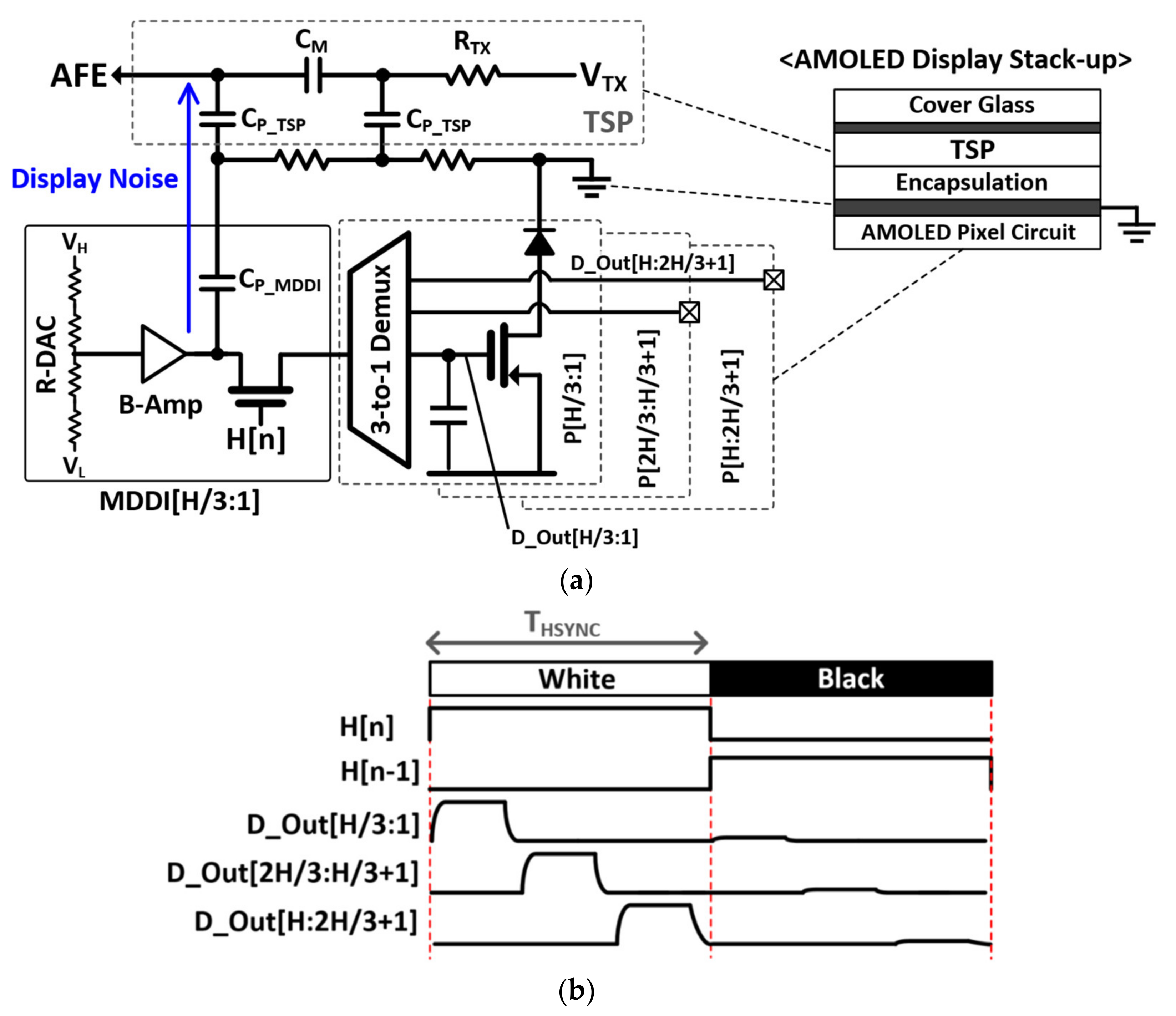
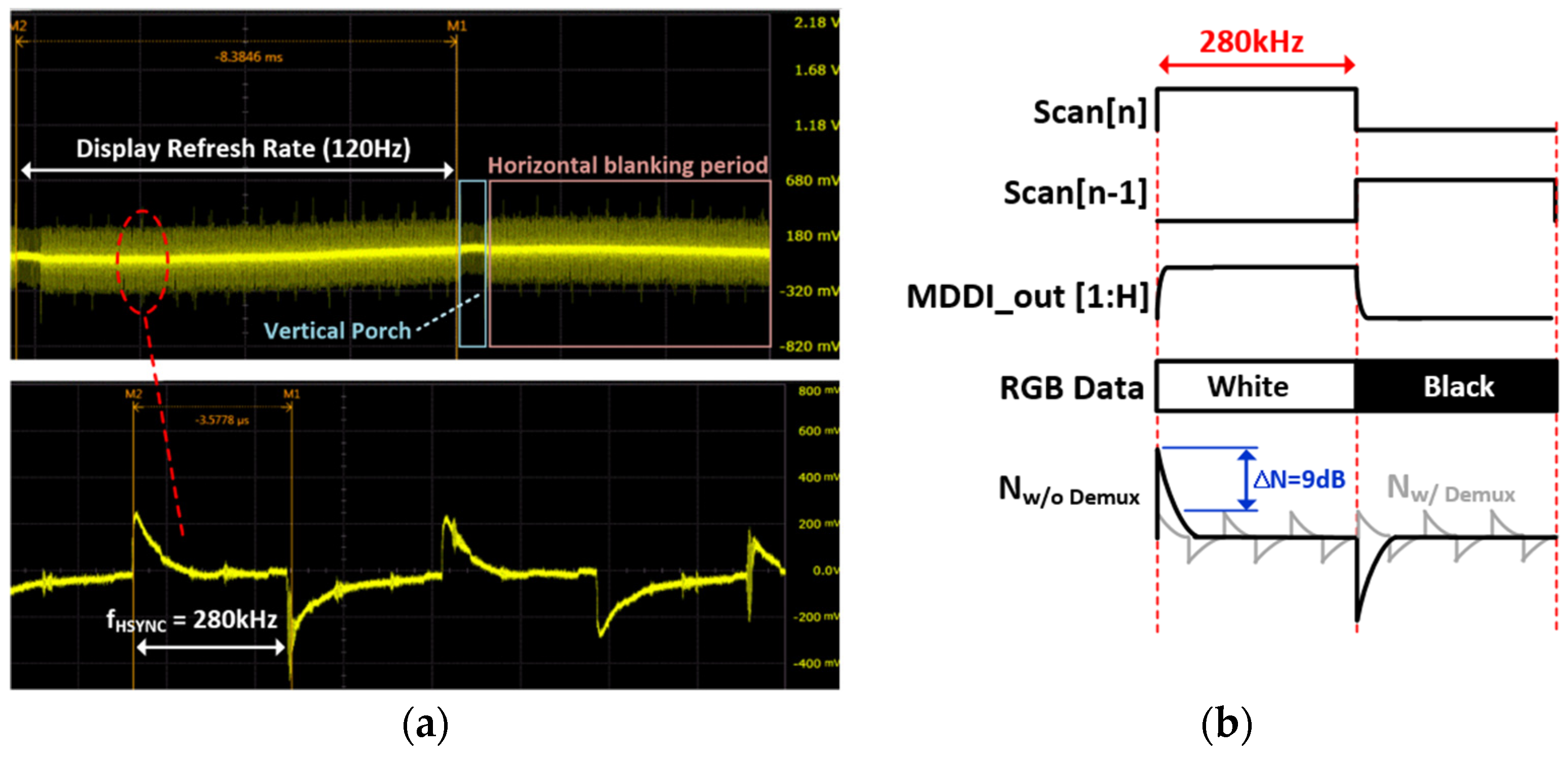
2.1. Display Noise Measurement

Figure 2 shows the display noise measured on a TSP electrode when a zebra pattern is updated onto a 2400 × 1080 FHD plus panel with a 120 Hz refresh rate. One horizontal (1-H) zebra pattern which alternates horizontal black and white colors at a time interval of THSYNC (=1/fHSYNC) was used for this measurement. In this case, we can approximately calculate the display noise frequency from the product of the refresh rate (120 Hz) and horizontal resolution (2400) of the panel. The maximum signal swing of the output of the MDDI (MDDI_ out[1:H]) occurs when it goes from black to white or from white to black horizontal lines. At those moments, display noise is also maximized. The noise waveform is a form of the derivative of a rectangular MDDI_Out, since the noise current flows across the series of CP_MDDI and CP_ TSP (Figure 1a). The harmonics of fHSYNC also exist in the noise signal frequency. Note that the noise frequency highly depends on the display contents to be updated, so it cannot be expected or removed by the frequency hopping scheme proposed in prior works. Compared with the HD panel which executes time-interleaved updates using 3-to-1 Demux in a THSYNC, the noise voltage increased by three times (9 dB), incurring a large noise penalty with a high-resolution, high-refresh-rate display.

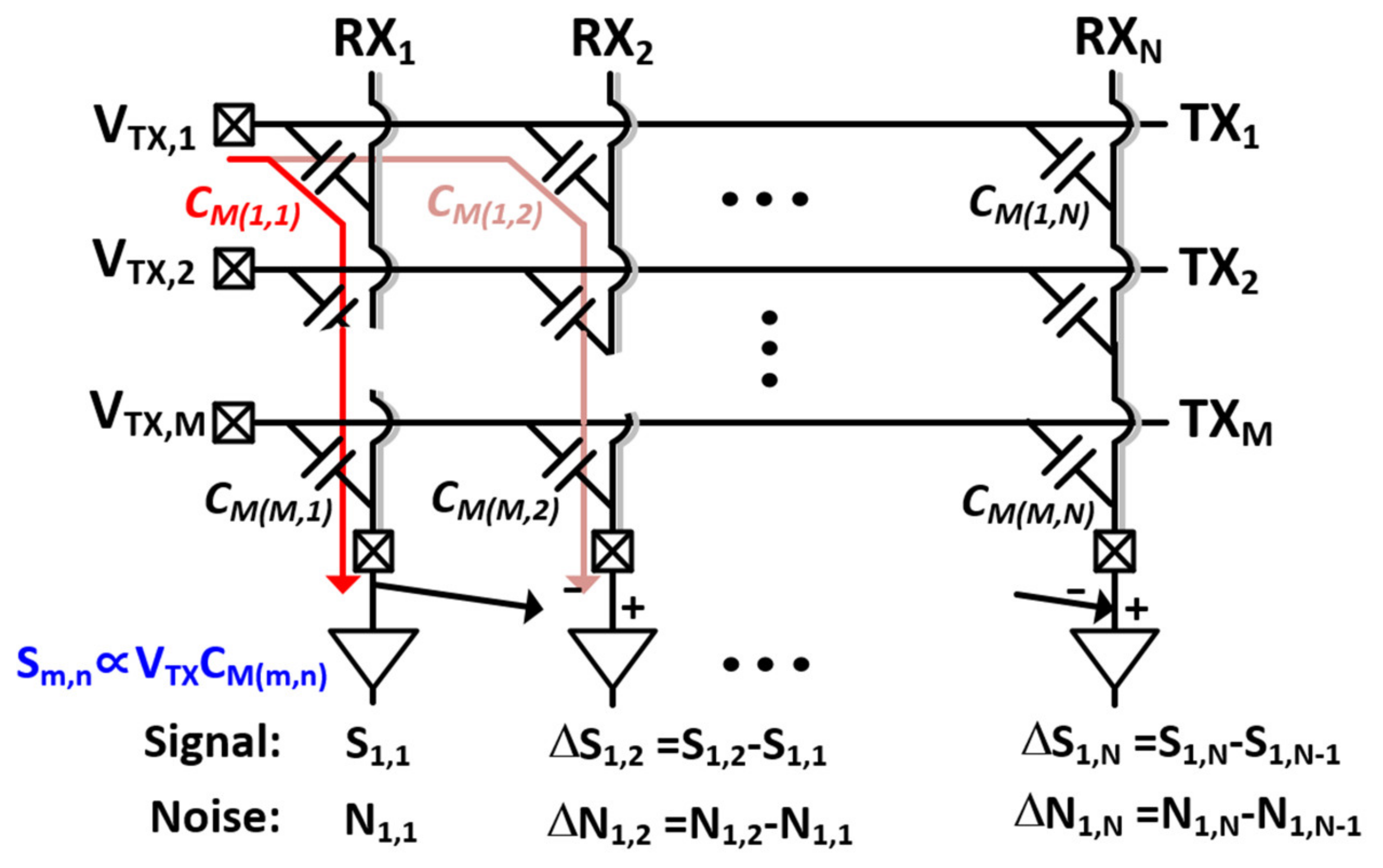
2.2. Basic Principle of Differential Sensing

The detailed operation of differential TSP sensing is shown in Figure 3. The TSP consists of M TX electrodes and N RX electrodes. An entire TSP channel is divided into the reference capacitance channels (CM(1,1)–CM(M,1)) in a, RX electrode, and the remaining capacitance channels (CM(1,2)–CM(M,N)) for differential sensing. The capacitance channel or mutual capacitance in a TSP is generated at the cross-section of each of the TX and RX electrodes. During the sensing phases for both differential and reference capacitance, the driver stimulates the TX electrodes (from TX1 to TXM) sequentially or concurrently using encoded TX signals (from VTX,1 to VTX,M). These signals are coupled through the mutual capacitance channel and measured at the RX electrode by the AFE. Therefore, touch sensitivity becomes proportional to the product of the mutual capacitance and the signal swing of the driver output. A simple dynamic buffer-generating square wave can be used as the TSP driver, reducing the design complexity. At the AFE, column-parallel differential sensing is usually employed to suppress common-mode noises, which include any external noises as well as the display interference. A fully or pseudo-differential trans-impedance amplifier or switched-capacitor integrator are used as a first AFE stage to detect only the capacitance difference (∆CM). At that moment, besides the ∆CM, the interferences are frozen on the first stage but are cancelled differentially. Post-processing of capacitance data to extract an exact touch coordinate requires that the ∆CM be recovered to a single-ended CM. We can execute an integral of the ∆CM of a column in a horizonal direction, which is based on the reference capacitance channels CM(1,1)–CM(M,1), in an RX electrode. Thus, the reference RX electrode acts like an integral basis and the recovered single-ended signals (SRCV(m, n)) for the CM(m,n) can be expressed as
S R C V m , n = S m , 1 + γ N m , 1 + k = 2 n S m , k + N m , k
where we assume that S m , 1 and N m , 1 are the capacitance and noise signals at the cross-section of the mth TX, and the 1st RX electrodes measured in a single-ended manner and S m , k and N m , k are the difference values of S m , k S m , k 1 and N m , k N m , k 1 , respectively. The attenuation ratio ( γ ) of Nm,1 needs special attention. If γ is equal to zero, N m , k can be suppressed by the differential operation. Otherwise, N m , 1 can be considered as a global noise component across all TSP channels in differential sensing.
This equation inspires us to choose and set the noise-immune reference capacitance channels, noise to which directly adds to the reconstructed capacitance value. Thus, the degree of noise suppression in a differential TSP sensing readout system depends on how much of the noise voltage is frozen in the reference capacitance channels.

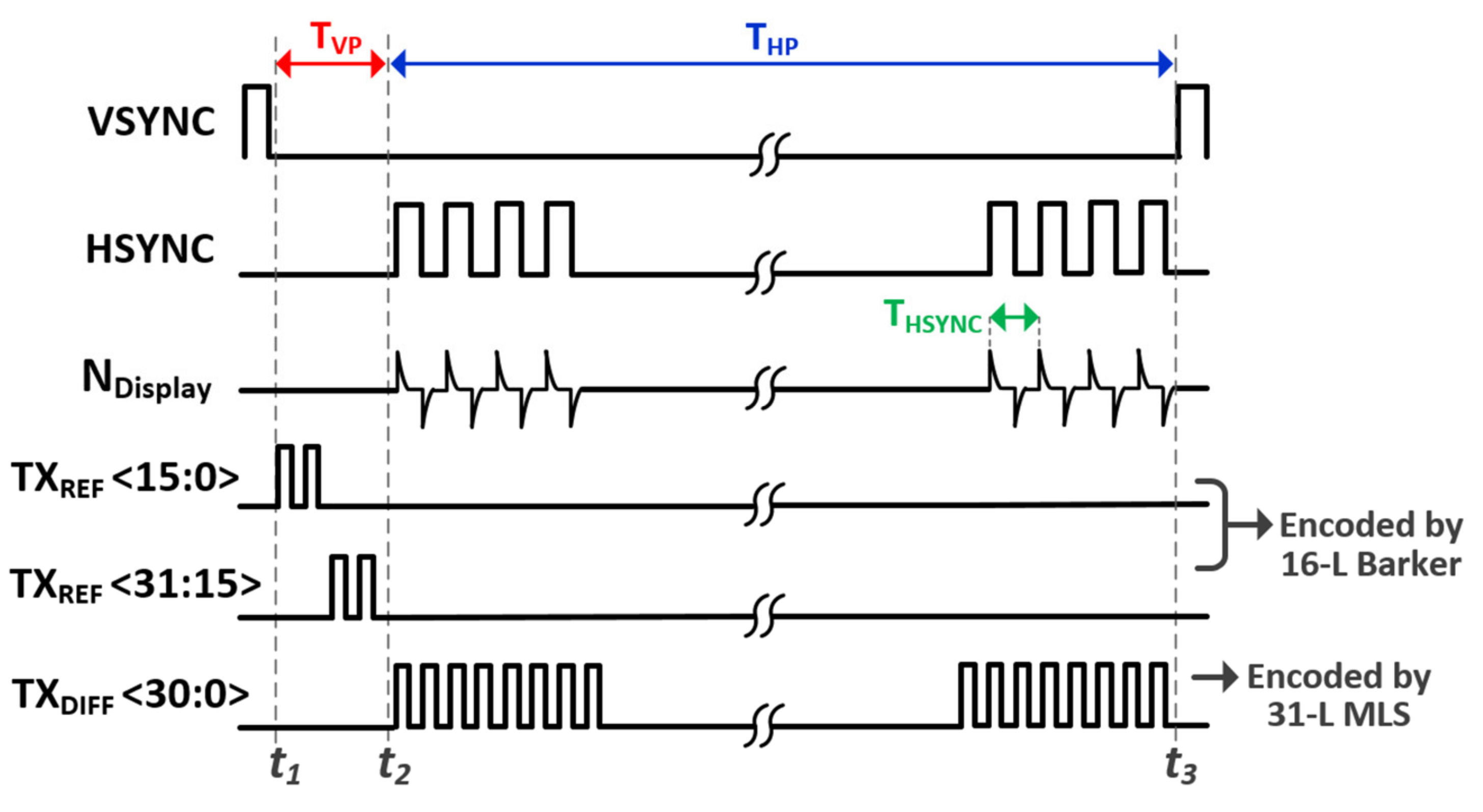
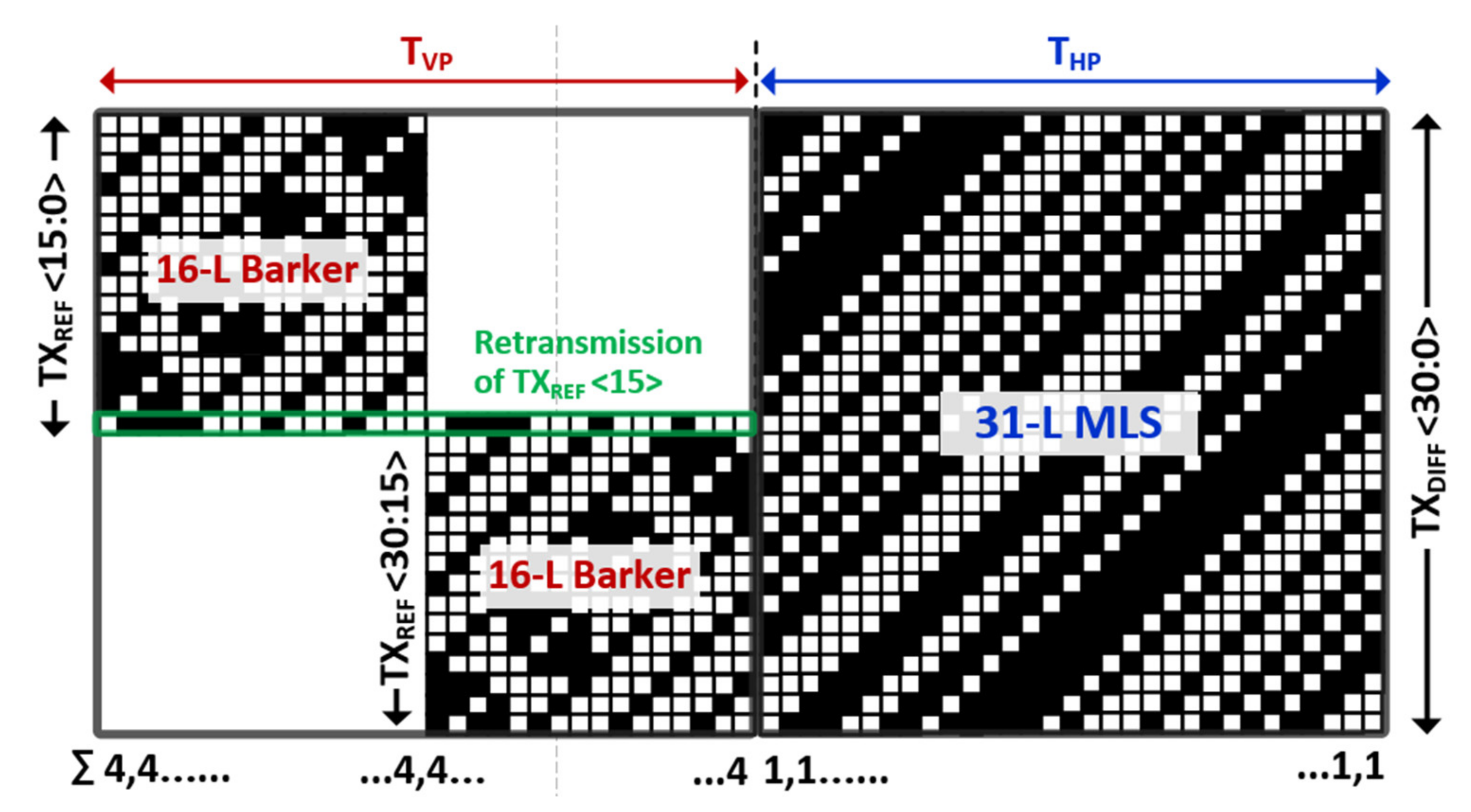
2.3. Detailed Operation of the Proposed Scheme

Figure 4 provides a timing diagram to illustrate our proposed differential TSP sensing mechanism. The display frame update repeats itself every vertical synchronization signal (VSYNC), where an entire MDDI operation cycle is divided into two phases: the vertical front porch (TVP) from t1 to t2, and the horizontal blanking period (THP) from t2 to t3. During TVP, the voltage of the cathode plane in the AMOLED is changed, which, in a mobile device, is dependent on the brightness of the display. Since the rate of change of the voltage is too slow, the noise current from the cathode plane to the TSP electrode, which passes through the parasitic capacitance of TSP (CP_TSP) (Figure 1a), is also insignificant. The AMOLED pixel voltage begins to vary from t2. As with high-refresh-rate, high-resolution panels, all RGB pixels P[H:1] in a horizontal line should be updated in a THSYNC, which is synchronous to the horizontal synchronization signal (HSYNC). In this case, the rising and falling time of the MDDI_out[H:1] should also decrease, leading to an amplified noise current insertion through the series of CP_MDDI and CP_ TSP to the TSP electrode. Total display noise is also proportional to the number of pixels (H) in a horizontal line to be updated. In this design, we take careful consideration in dealing with the timing of the reference and differential capacitance driving. The reference capacitance channels in an RX electrode are driven by TXREF <30:0> during TVP. This is because the display noise is negligible compared with that during THP. On the other hand, a column-parallel capacitance difference is measured during THP. The common noise voltage freezes to both the positive and negative paths of the differential sensing AFE, but is cancelled differentially. By separating the sensing phases of the reference and differential capacitance, an improved SNR is achieved for its reference capacitance against the display noise, and sufficiently long THP helps to suppress any external noises [12,13] besides the display noise.
Different orthogonal sequences, TXREF <30:0> and TXDIFF <30:0>, were employed for the driving of the reference and differential capacitances. When we introduced the orthogonal driving into the TSP readout system [14,15,16], we faced a tradeoff between dynamic range and crosstalk. Although the multi-channel driven concept increased the sensing time for each TSP channel, leading to increased sensitivity, total capacitance to be processed by the AFE also increased. This limited the dynamic range of the AFE and increased the burden to the operation amplifier from the trans-impedance amplifier or the switched capacitor integrator, which are the first stage of AFE. For a Hadamard orthogonal sequence, the vertical code summation becomes equal to the number of orthogonal sequences. One method is to use another orthogonal sequence that minimizes the code summation, but it is at the expense of increased residue between the TSP channels in adjacent TX electrodes, where the residue can be defined by the inner product of orthogonal sequences. In case of the n-length (n-L) maximum-length orthogonal sequence (MLS) [17,18], the inner product is equal to n when inner product with itself is done. However, the inner product for different MLSs is reduced to 1, regardless of length. Thus, the crosstalk can be calculated to 1 divided by n, or by the code-length of the MLS.
In a practical design, when an FHD and an AMOLED having a 31 TX and 16 RX electrode TSP was evaluated, we applied a different orthogonal encoding method during the TVP and THP, as shown in Figure 5. Firstly, during TVP for reference capacitance sensing, there are also two sensing phases: the upper TSP sensing phase, and the lower TSP sensing phase. The reasons are twofold. First, the panel bandwidth (fTBW_UPPER) of the upper TSP area is much smaller than that of the lower TSP area. Thus, the TX driver experiences the greatest delay when it transfers the charge of CM(1,1) (in Figure 3) from TX [1] to RX [1]. This phase mismatch would disrupt the orthogonality if we were to choose a higher TX frequency free from external noises besides the display noise. Second, code summation should be minimized while maintaining perfect orthogonality between each TX electrode, which is highly desirable to set the integral basis for differential sensing. To achieve a reasonable tradeoff, a 16-length baker sequence [19,20] was applied to TXREF <0:15> and TXREF <15:31>. Here, TXREF <15> was retransmitted for the lower TSP area, which can balance the code summation to four without incurring crosstalk.
During THP, all TX electrodes are driven simultaneously by the 31-L MLSs, which is desirable for two reasons. First, display noise due to the RGB pixel updates in the THP does not saturate the AFE since the code summation is reduced to one mutual capacitance unit (CM). Second, the SNR increases by the square root of 31 compared with that of sequential driving. Although the TX frequency is restricted to be much lower than the fTBW_UPPER and crosstalk exists between the TX electrodes, this noise penalty can be suppressed by permitting differential capacitance sensing.
In the TSP readout system, the inner product for TXREF <30:0> and TXDIFF <30:0> can be found to be
T X REF < i >   · T X REF < j > = 16   i = j 0   i j
T X DIEF < i >   · T X DIEF < j > = 31   i = j 1   i j

3. Circuit Implementations

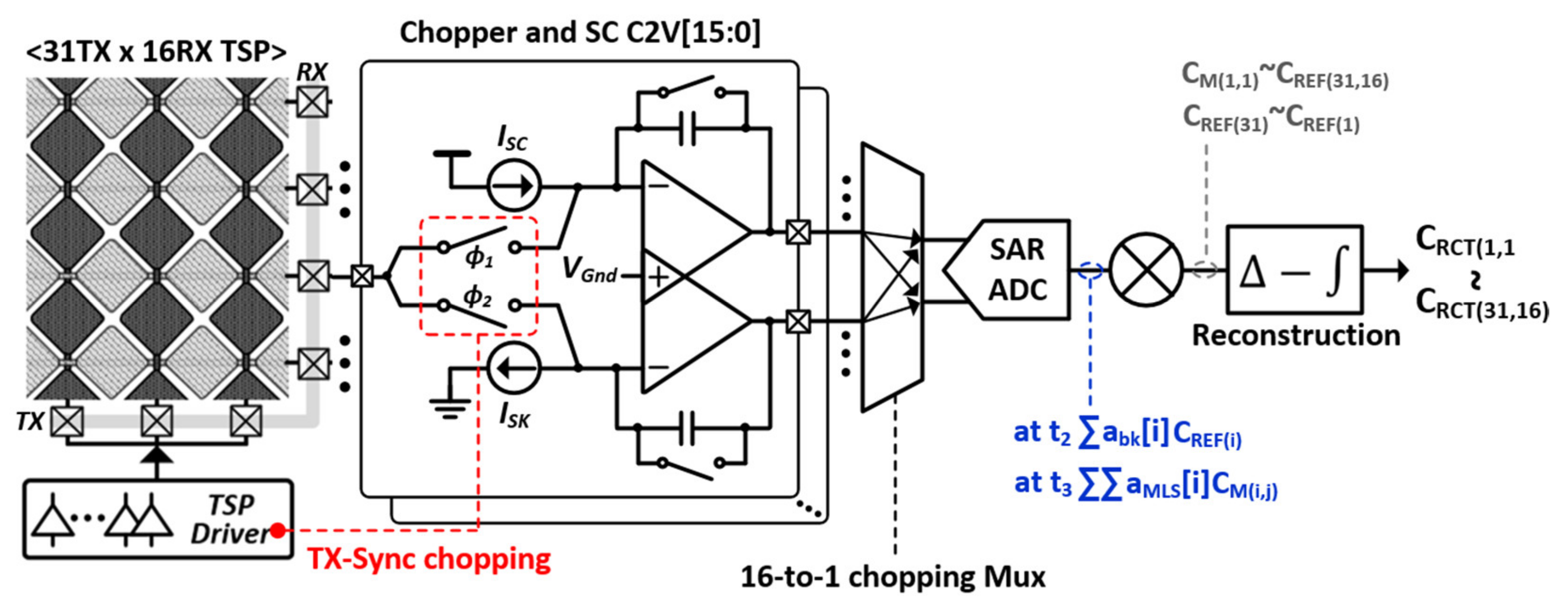
3.1. Whole Readout System Architecture

Figure 6 shows the proposed TSP sensing architecture, where it senses the mutual capacitance of 31 TX electrodes and 16 RX-TSP electrodes. It is comprised of a TSP driver, a switched capacitor integrator for capacitance-to-voltage (C2V) conversion, a successive approximation register (SAR) analog-to-digital converter (ADC), and decoding and reconstruction logic. During the reference capacitance sensing phase (TVP), the TSP driver stimulates the TX electrode by TXREF <30:0>. The TX carrier frequency is encoded by a 16-L Barker sequence, and the upper and lower TSP areas are driven separately. When the TVP finishes, all TX electrodes are driven simultaneously by TXDIFF <30:0>, which is encoded by 31-L MLS. To suppress external and display coupling noise, the sensing time should be sufficiently long, thus occupying most of the THP for differential sensing. At the same time, the front-end executes column-parallel TSP sensing with 16 C2V converters (C2V[15:0]). Besides conversion, a C2V converter acts as a discrete-time bandpass filter whose passband is centered on the TX frequency. The base capacitance, which is unchanged by the touch of a finger, is cancelled through a current compensation technique, where the sink (ISK) or source (ISC) current is provided to the AC-modulated capacitance signals at the C2V input. The voltage of the virtual ground of the C2V converter is fixed to half of the supply voltage, but exhibits an offset. In case of a panel having a large CP_TSP, it can saturate the output of a C2V. This risk can be removed by a chopping scheme where the phase of a TX signal is synchronous to the closing of ϕ1, ϕ2, and a 16-to-1 bidirectional ADC multiplexer (Mux).
The system adopts a differential sensing scheme processed in a digital domain. The reasons are twofold. First, in a practical design, we should sense both a single ended reference capacitance and the capacitance difference. Thus, we can choose the same input stage to sense both. Moreover, compared with previous work enabling higher-order band pass filtering with multiple AFE stages in an analog domain, it can ease the power and area budget of the IC with only two op-amps in the CDS. Second, compared with previous works, it can increase the sensing time by two times compared with differential AFE sensing. For simplicity of explanation, let us consider when the differences of CM(1,1), CM(1,2), and CM(1,3) are sensed directly at the AFE. In this case, after the difference between CM(1,1) and CM(1,2) is sensed, that of CM(1,2) and CM(1,3) should be sensed sequentially to reconstruct the single-ended capacitance. This lowers the sensitivity by 3 dB compared with differential processing in the digital domain. This way, the insufficient noise filtering of differential sensing in digital domain can be supplemented. With a reference capacitance of CREF(31)–CREF(1) and a single-ended measured capacitance of CM(1,1)–CM(31,16), the final output corresponding to CRCT(1,1)–CRCT(31,16) can be obtained.

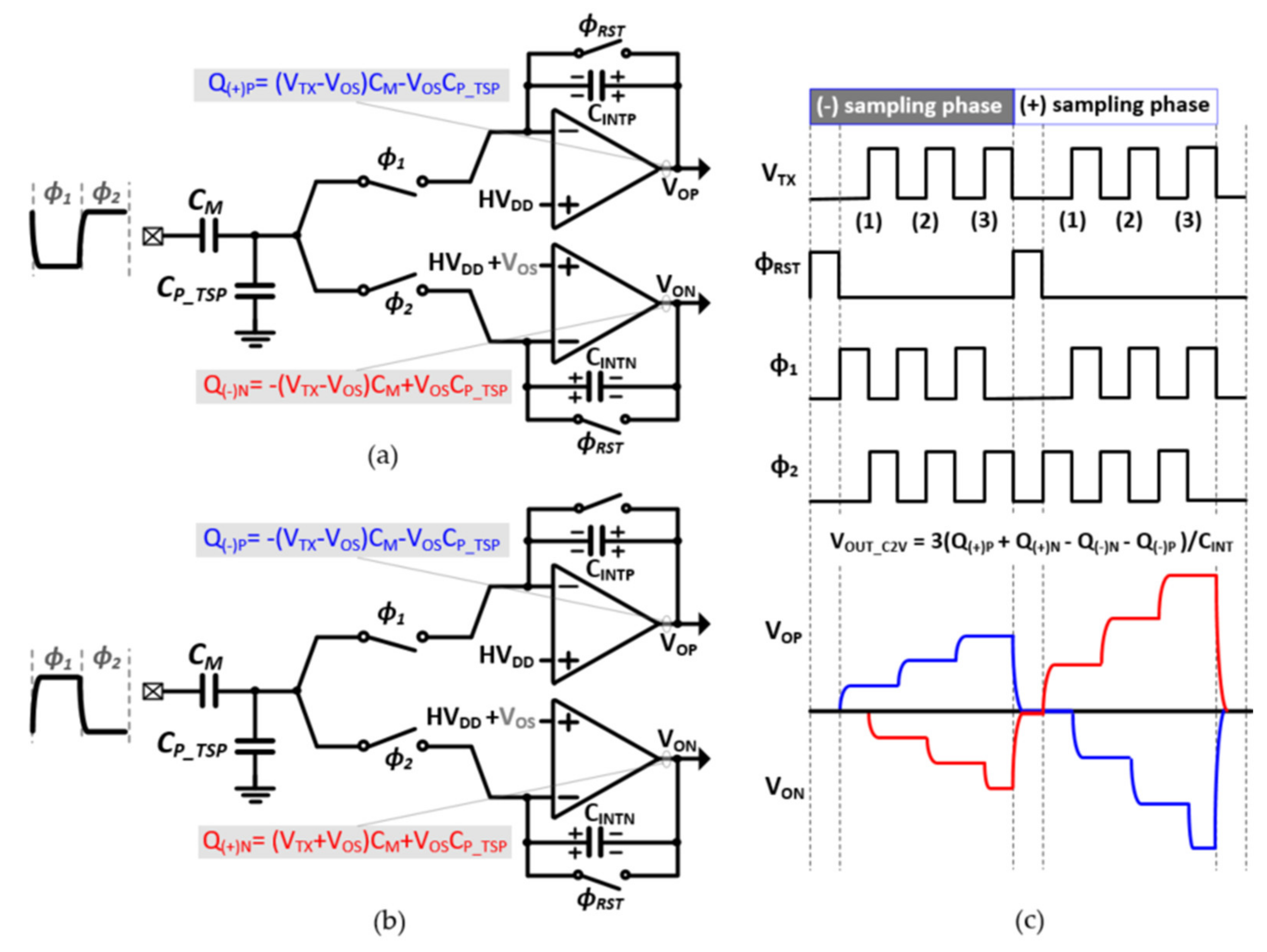
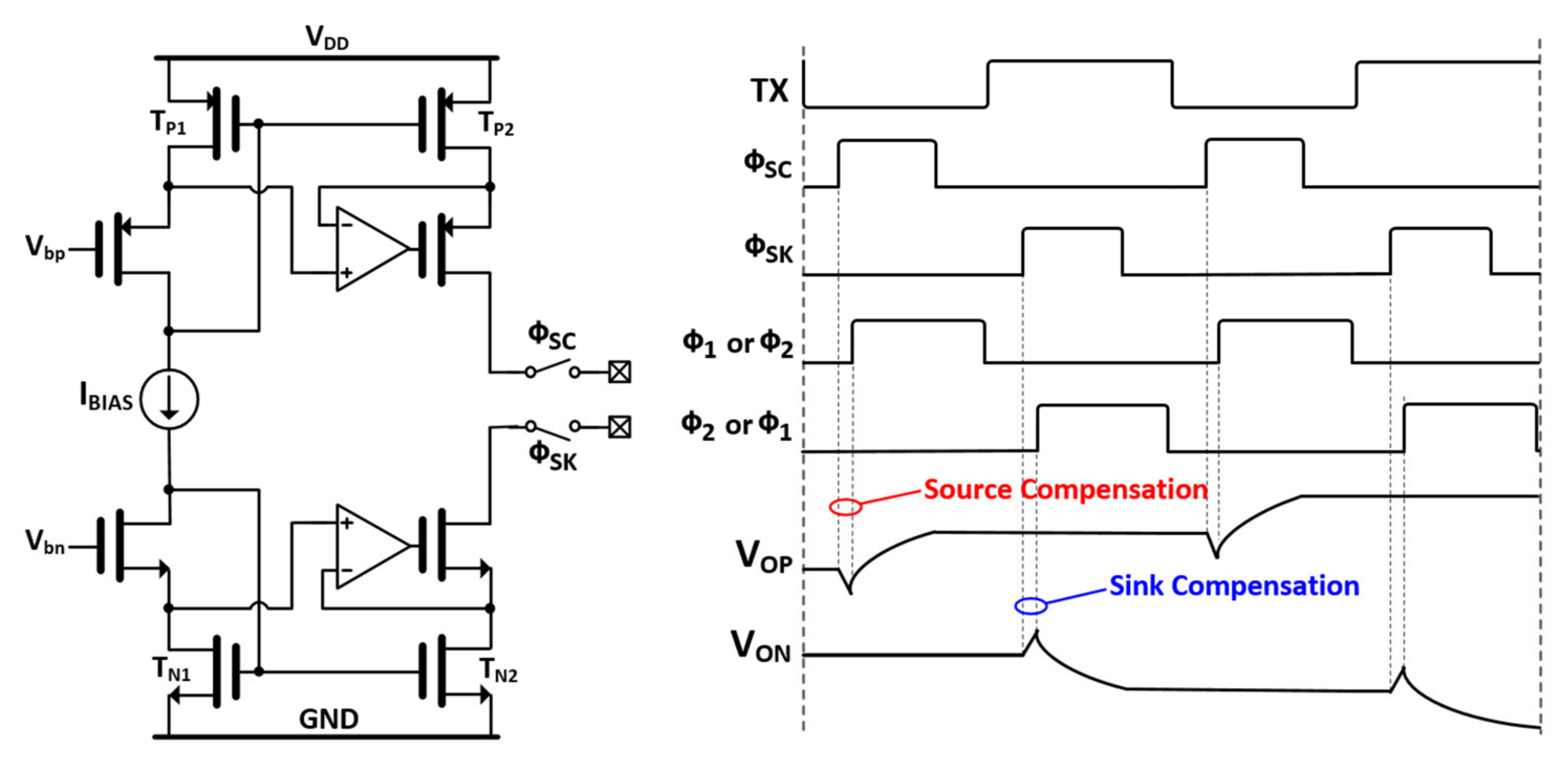
3.2. Input Offset Cancellation and Capacitance Compensation Techniques

Figure 7a–c shows the detailed operation of the proposed C2V converter with the input offset cancellation technique. The C2V converter consists of positive and negative switched capacitor (SC) integrators and sampling switches at the inputs. When ϕRST is high, the VOP and VON are reset to half of supply voltage. As ϕRST falls, the charge on the mutual capacitance CM is transferred to the integral capacitors of CINTP and CINTN. When ϕ1 is high and VTX is low, the charge proportional to CMVTX is trapped on the ride-side of CINTP, increasing the VOP. Then, when both ϕ2 and VTX are high, the negative charge of CMVTX is transferred to the ride-side of CINTN, decreasing the VON. By repeating itself every TX sample, moving-average bandpass filtering in the analog domain is obtained [21].
However, as the thickness of the AMOLED panel decreases, the TSP electrode becomes close to the display pixels, leading to the increased parasitic capacitance of CP_TSP. For encapsulation glass with a thickness of about 100 μm, the CP_TSP is increased to tens of picofarads. In this case, C2V can saturate as the number of moving average taps increases. Let us consider that the (+) input of a positive SC integrator in the C2V converter is higher than that of the negative SC integrator by VOS. When ϕ1 is high, the CP_TSP is charged to half of the supply voltage. Then, when ϕ1 is low and ϕ2 is high, the total charge on the CP_TSP increases by CP_TSPVOS, bringing an equal positive charge to the right-hand side of CINTN. Since these offsets can be varied from C2V[15:0], it degrades sensing accuracy and saturates the AFE. For example, with 100 μF of CP_TSP, 2 μF of CM, 3, of TSP excitation signal, and 10, V of input offset voltage, an offset charge of 10 μC is also introduced, which is one-sixth of the charge from mutual capacitance. To minimize a circuit’s offset without any additional circuits, offset cancellation chopping is employed, which uses RX-correlated TSP driving.
The sensing phase is divided into two phases: the positive (+) offset sampling phase and the negative (−) offset sampling phase. During the negative sampling phase, when ϕ2 is high, VTX goes high. Therefore, a negative offset charge is stored on the CINTP while positive (VTX–VOS)CM is frozen on it, and vice versa for CINTN. The offset charge of VOSCM is insignificant compared with that of VOSCP_TSP. During the positive sampling phase, when ϕ1 is high, VTX goes high. In this case, the negatives of both the CM-charge and the offset charge are stored on the CINTP, and vice versa for CINTN as well. To cancel the offset voltage at the C2V output, the VOP in the positive sampling phase adds to the VON in the negative sampling phase. This can be enabled by reversing the connection in the 16-to-1 ADC Mux. The operational amplifier in the switched capacitor integrator is a two-stage class AB amplifier. Based on post-layout simulations, the amplifier achieves a DC gain of 61 dB and unity gain bandwidth of 12MHz while consuming 140 μW power from a 3.3 supply.
During the sensing phase for both the TVP and THP, the base capacitance, which is not unchanged by a finger touch and occupies most of the dynamic range of AFE, should be removed. The detailed operation of the compensation circuit used here is shown in Figure 8 [20]. When ϕSC is high, the positive charge from the ISC is provided to the negative input of a switched capacitor integrator. When ϕSK is high, the ISK, which is equal to the ISC, flows from its negative input. Since the TSP electrode is driven by AC signals, ISK and ISC repeat every high and low state of the TX signal. The DC bias current (IBIAS) is copied into the TP1 and TN1 and amplified N times by TP2 and TN1, respectively. In a practical design, a minimization of the mismatch between ISK and ISC is required. Thus, to minimize the channel length modulation effect, the VDS of TP1 and TP2, and the VDS of TN1 and TN2 are fixed to be equal using a regulated cascode feedback amplifier. Specifically, the phase of ϕSK or ϕSC leads that of ϕ1 or ϕ2, preventing a disturbance of the negative input voltage due to the charge transfer of CM when compensation starts. In a practical design, the delay is fixed to a time duration of 5/fMAIN where fMAIN is 40 MHz or the operational clock of MCU in the designed IC.

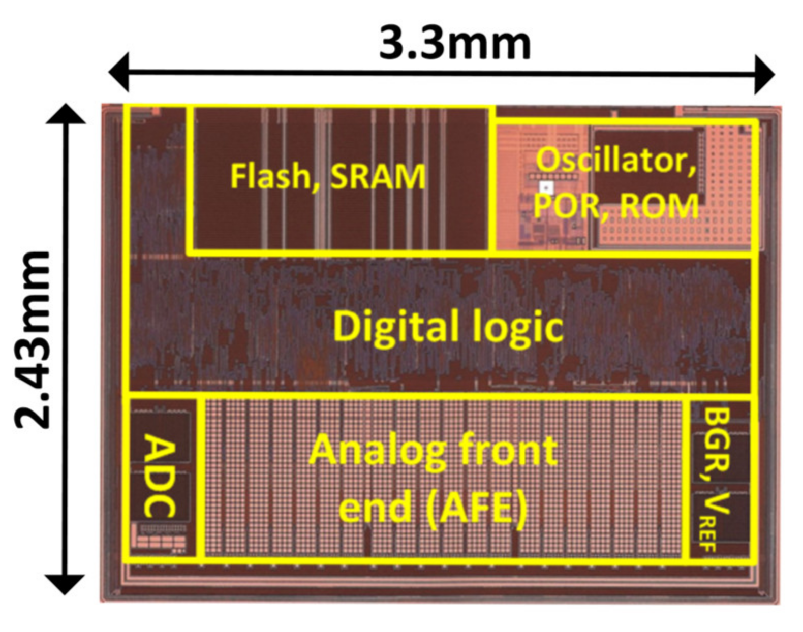
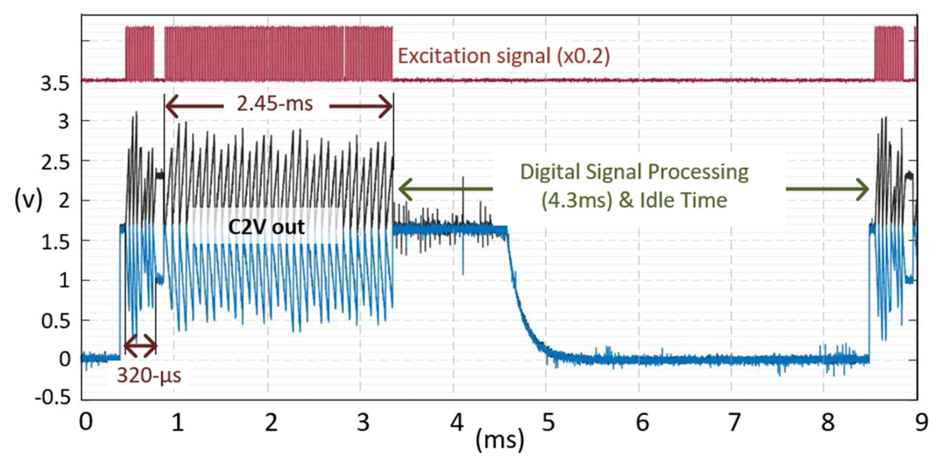
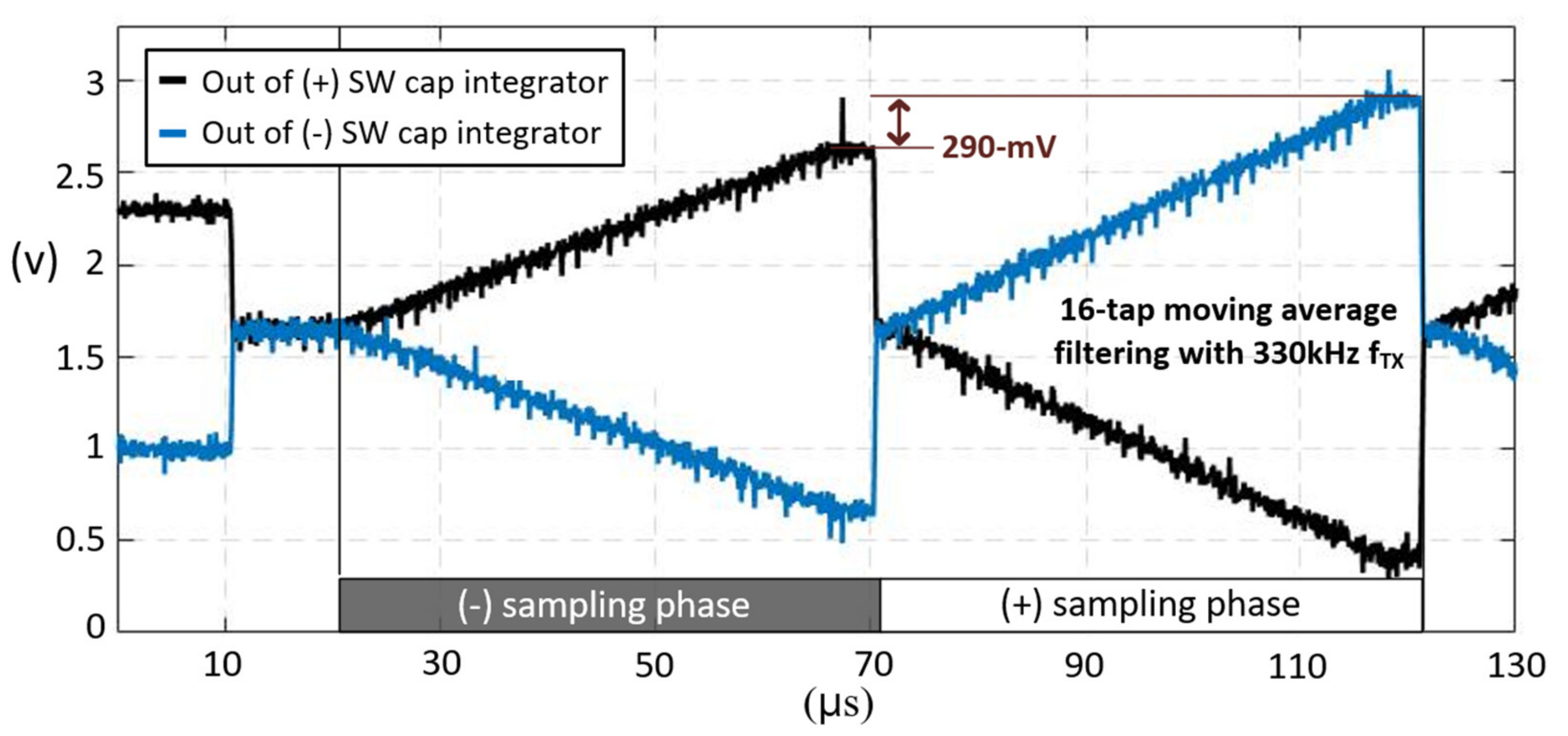
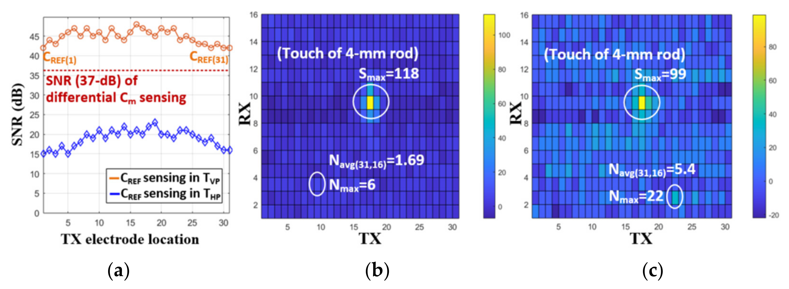
4. Result and Discussion

The proposed readout IC was fabricated in a 130-nm CMOS process. The die photograph is shown in Figure 9. The active area, which includes the AFE, SAR ADC, bandgap reference (BGR), and reference voltage generator (VREF), is 3.4 mm2 and the full chip area is 8.02 mm2. TSP driving was synchronized with the display update, where its frame rate is measured to be 123 Hz with a 2400 × 1080 FHD plus 6.1-inch AMOLED panel. For a TSP having 31 TX and 16 RX electrodes, the total power consumption was 17.1 W with a 3.3, power supply. The power breakdown for the AFE was 6.4 W. Operating the AFE only during part of a frame reduced its power consumption. Here, the AFE scan time was reduced to 3 ms, including the reference capacitance and differential capacitance sensing phases.
Figure 10 shows the measured TX signal and C2V output in a TSP frame. The sensing phase for reference capacitance sensing was 320 μs, while the differential sensing time was set to be 2.45 ms. Since touch coordinates should be extracted and provided to the application processor in a smartphone every TSP frame (123 Hz), digital signal processing time for interpolation, coordinate filtering, and baseline calibration is needed, and was set to be 4.3 ms. Figure 11 provides the measured C2V output before the 16-to-1 ADC multiplexer when the input offset cancellation technique was applied. The TX frequency of 330 kHz and a 16-repetition of the TX pulse were used for measurement. One orthogonal instant was divided into (+) and (−) sampling phases. The output voltage difference or offset voltage between these phases was 290 mV, which would be eliminated by adding outputs in each phase. To evaluate the effectiveness of sensing in TVP, the reference capacitance (Cref(1)~Cref(31)) was measured during both TVP and THP, as shown in Figure 12a where the 1-H zebra image was updated. The SNR measured in the TVP was 22 dB higher than that of the THP, since any display signals related to the 1-H zebra image did not exist during TVP. Figure 12b,c shows the differential and single-ended measured touch profile when a 4 mm diameter conductive rod was touched, with a display update from 1-H zebra image. Here, the touch data was RMS-averaged over 1000-frames. The noise values of the THP (Nmax, Navg(31,16)) were more than three times larger than that of the TVP. The SNR for differential sensing was measured to 37 dB, while that of single-ended sensing was 25.4 dB. The SNR loss between the reference capacitance and the differential capacitance sensing was 9 dB (Figure 12a). This is because the coupled display noises at each RX electrode have a mismatch in phase and amplitude. The performance summary and comparison with previous works are shown in Table 1. Unlike other state-of-the-art works, it describes noise-immunity to display noise and suppresses it by 37 dB in the worst possible case. Although other works achieved better SNR, a metal-mesh TSP sensor has higher capacitive change according to touch. The metal-mesh sensor also has smaller TSP-series resistance, allowing the use of a higher TSP frequency.

5. Conclusions

This article describes a display-noise-immune TSP readout system with synchronization of touch and display driving. It reduces the display noise by more than 4 times and has a compact structure without any additional circuits for differential sensing. The tradeoff between dynamic range and crosstalk is eased by introducing different orthogonal encoding for reference and differential sensing.
This technique is applicable to other display architectures. It can be easily adopted in an LCD or flexible AMOLED where the vertical porch and horizontal update instants exist.

Funding

The present research was conducted with funding by the Research Grant of Kwangwoon University in 2021.

Conflicts of Interest

The author declares no conflict of interest.

References

  1. Galaxy S21 Ultra 5G. Available online: https://www.samsung.com/global/galaxy/galaxy-s21-ultra-5g/specs/ (accessed on 19 June 2021).
  2. Galaxy Tab S7. Available online: https://www.samsung.com/global/galaxy/galaxy-tab-s7/ (accessed on 19 June 2021).
  3. How Do You Use Always on Display Mode on Galaxy S20, S20+, S20 Ultra, and Z Flip? Available online: https://www.samsung.com/global/galaxy/what-is/always-on-display/ (accessed on 19 June 2021).
  4. David, W. Capacitive Sensing: Ins and Outs of Active Shielding. Available online: https://www.ti.com/lit/an/snoa926a/snoa926a.pdf?ts=1627473795125&ref_url=https%253A%252F%252Fwww.google.com%252F (accessed on 25 July 2021).
  5. Kim, H.R.; Choi, Y.-K.; Byun, S.-H.; Kim, S.-W.; Choi, K.-H.; Ahn, H.-Y.; Park, J.-K.; Lee, D.-Y.; Cho, H.-H.; Yu, J.-S.; et al. A Mobile-Display-Driver IC Embedding a Capacitive-Touch-Screen Controller System. In Proceedings of the International Solid–State Conference Digest of Technical Papers (ISSCC), San Francisco, CA, USA, 7–11 February 2010; pp. 114–116. [Google Scholar]
  6. Hotelling, S.P.; Krah, C.H.; Huppi, B.Q. Multipoint Touch Surface Controller. U.S. Patent 8 279 180, 2 October 2012. [Google Scholar]
  7. Huang, S.-L.; Hung, S.-Y.; Chen, C.-P. Frequency hopping and parallel driving with random delay especially suitable for the charger noise problem in mutual–capacitive touch applications. IEEE Access 2018, 7, 3980–3993. [Google Scholar] [CrossRef]
  8. Park, J.-E.; Lim, D.-H.; Jeong, D.-K. A reconfigurable 40–to–67 dB SNR, 50–to–6400 Hz frame–rate, column–parallel readout IC for capacitive touch–screen panels. IEEE J. Solid-State Circuits 2014, 49, 2305–2318. [Google Scholar] [CrossRef]
  9. Hamaguchi, M.; Nago, A.; Miyamoto, M. A 240 Hz–Reporting Rate 143 × 81 Mutual-Capacitance Touch–Sensing Analog Front–End IC with 37 dB SNR for 1 mm–diameter Stylus. In Proceedings of the International Solid–State Circuits Conference Digest of Technical Papers (ISSCC), San Francisco, CA, USA, 9–13 February 2014; pp. 214–216. [Google Scholar]
  10. Kim, K.-D.; Kang, S.; Choi, Y.-K.; Lee, K.-H.; Lee, J.-C.; Choi, M.; Ko, K.; Jung, J.; Park, N.; Park, H.; et al. A Fully–Differential Capacitive Touch Controller with Input Common–Mode Feedback for Symmetric Display Noise Cancellation. In Proceedings of the IEEE Symposium on VLSI Circuits, Honolulu, HI, USA, 10–13 June 2014; pp. 1–2. [Google Scholar]
  11. Lee, C.-J.; Park, J.K.; Seo, H.-E.; Huh, J.; Chun, J.-H. Fully differential touch screen controller with wide input dynamic range for thin displays. Sensors 2020, 20, 837. [Google Scholar] [CrossRef] [PubMed] [Green Version]
  12. Klein, K. Noise Immunity of Touchscreen Devices. Available online: http://www.cypress.com/file/120641/download (accessed on 25 July 2021).
  13. Nam, H.; Seol, K.-H.; Lee, J.; Cho, H.; Jung, S.W. Review of capacitive touchscreen technologies: Overview, research trends, and machine learning approaches. Sensors 2021, 21, 4776. [Google Scholar] [CrossRef] [PubMed]
  14. Lee, C.-J.; Park, J.; Seo, H.-E.; Huh, J.; Chun, J.-H. A mutual capacitance touch readout IC with 64% reduced-power adiabatic driving over heavily coupled touch ccreen. IEEE J. Solid-State Circuits 2019, 54, 1694–1704. [Google Scholar]
  15. Park, J.-E.; Park, J.; Hwang, Y.-H.; Oh, J.; Jeong, D.-K. A noise–immunity–enhanced analog front–end for 36 × 64 touch–screen controllers with 20–VPP noise tolerance at 100 kHz. IEEE J. Solid State Circuits 2019, 54, 1497–1510. [Google Scholar] [CrossRef]
  16. Ko, S. A–24 dB in-band noise-immunity mutual capacitance readout system for variable refresh rate of active-matrix OLED display. IEEE Trans. Circuits Syst. I Regul. Pap. 2020, 67, 1126–1135. [Google Scholar] [CrossRef]
  17. Dinan, E.H.; Jabbari, B. Spreading codes for direct sequence CDMA and wideband CDMA cellular networks. IEEE Commun. Mag. 1998, 36, 48–54. [Google Scholar] [CrossRef]
  18. Shin, H.; Ko, S.; Jang, H.; Yun, I.; Lee, K. A 55 dB SNR with 240 Hz Frame Scan Rate Mutual Capacitor 30 × 24 Touch–Screen Panel Read–Out IC Using Code-Division Multiple Sensing Technique. In Proceedings of the International Solid-State Circuits Conference Digest of Technical Papers (ISSCC), San Francisco, CA, USA, 17–21 February 2013; pp. 388–390. [Google Scholar]
  19. Golomb, S.W.; Scholtz, R.A. Generalized barker sequences. IEEE Trans. Inf. Theory 1965, 11, 533–537. [Google Scholar] [CrossRef]
  20. Ko, S. An Automatic Ear Detection Technique in Capacitive Sensing Readout IC Using Cascaded Classifiers and Hovering Function. In Proceedings of the Symposium on VLSI Circuits, Kyoto, Japan, 9–14 June 2019. [Google Scholar]
  21. Ko, S.; Shin, H.; Lee, J.; Jang, H.; So, B.-C.; Yun, I.; Lee, K. Low Noise Capacitive Sensor for Multi–Touch Mobile Handset’s Applications. In Proceedings of the Asian Solid-State Circuits Conference, Beijing, China, 8–10 November 2010; pp. 1–4. [Google Scholar]
  22. Lee, C.-J.; Park, J.K.; Piao, C.; Seo, H.-E.; Choi, J.; Chun, J.-H. Mutual capacitive touch screen controller for ultrathin display with extended signal passband using negative capacitance. Sensors 2018, 18, 3637. [Google Scholar] [CrossRef] [PubMed] [Green Version]
Figure 1. (a) An equivalent circuit consisting of an AMOLED, a TSP and an MDDI, and (b) a timing diagram of the MDDI operation using a 3-to-1 demultiplexer.
Micromachines 12 00922 g001
Figure 2. (a) Measured display noise with an FHD+ AMOLED display, and (b) comparison of display noise levels with a zebra image without Demux and with a 3-to-1 Demux configuration.
Micromachines 12 00922 g002
Figure 3. Illustration of the operation principle of a differential TSP sensing scheme.
Micromachines 12 00922 g003
Figure 4. Timing diagram for illustrating the proposed differential TSP sensing scheme.
Micromachines 12 00922 g004
Figure 5. Application of different orthogonal sequences in reference and differential capacitance sensing.
Micromachines 12 00922 g005
Figure 6. Proposed TSP-DDI synchronous differential front-end architecture.
Micromachines 12 00922 g006
Figure 7. C2V configuration for (a) the negative offset sampling phase (ϕ1 = high, VTX = low), (b) the positive offset sampling phase (ϕ1 = high, VTX = high), and (c) its timing diagram.
Micromachines 12 00922 g007
Figure 8. Circuit implementation of a capacitance compensator and its timing diagram.
Micromachines 12 00922 g008
Figure 9. Die Photograph.
Micromachines 12 00922 g009
Figure 10. Measured waveforms of the TX signal (red) and the C2V output (black and blue) when synchronizing TSP and MDDI driving.
Micromachines 12 00922 g010
Figure 11. Measured waveforms of the C2V output when the chopping scheme is applied.
Micromachines 12 00922 g011
Figure 12. (a) Comparison of SNR for reference capacitance (CREF) during TVP and THP, and the measured RMS touch profile of (b) the proposed differential TSP sensing and (c) conventional single-ended sensing.
Micromachines 12 00922 g012
Table 1. Performance summary and comparison to previous works.
This WorkRef. [14]Ref. [15]Ref. [22]
Process130 nm180 nm180 nm350 nm
Electrodes31 TX and 16 RX16 TX and 33 RX36 TX and 64 RX15 TX and 10 RX
Scan rate330 Hz
(Synchronous to 120 Hz AMOLED)
120Hz85~385Hz250 Hz
Power Consumption6.4 mW (AFE)
17.1 mW (Full chip)
17.8 mW67.7 mW12.8 mW
Chip area3.4 mm2 (AFE)
8.02 mm2 (Full chip)
7.1 mm236 mm24.89 mm2
SNR46 dB without display noise
37 dB with zebra pattern in 120 Hz AMOLED
57 dB54 dB43 dB
TSP TypeITOMetal MeshITOMetal Mesh
Publisher’s Note: MDPI stays neutral with regard to jurisdictional claims in published maps and institutional affiliations.

