
Research on Trimming Frequency-Increasing Technology for Quartz Crystal Resonator Using Laser Etching

 ,
,
Abstract
:1. Introduction
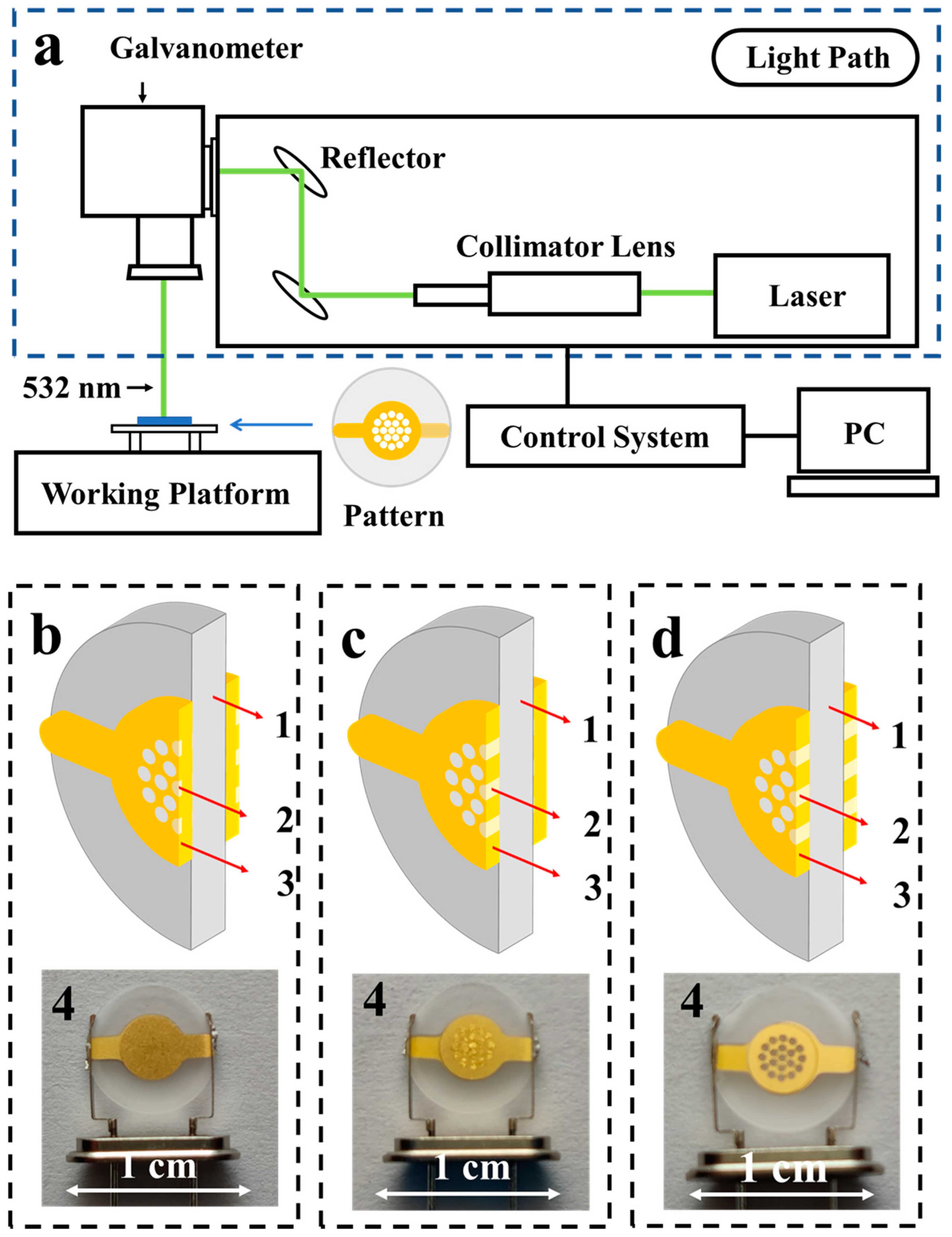
2. Experiment
3. Result and Discussion
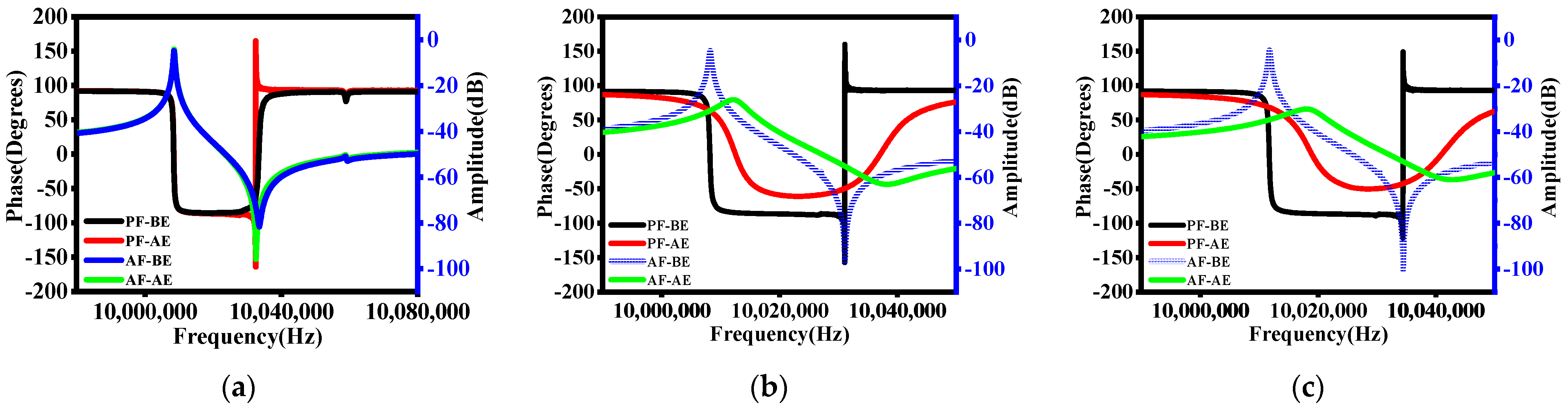
3.1. Amplitude–Frequency and Phase–Frequency Characteristics
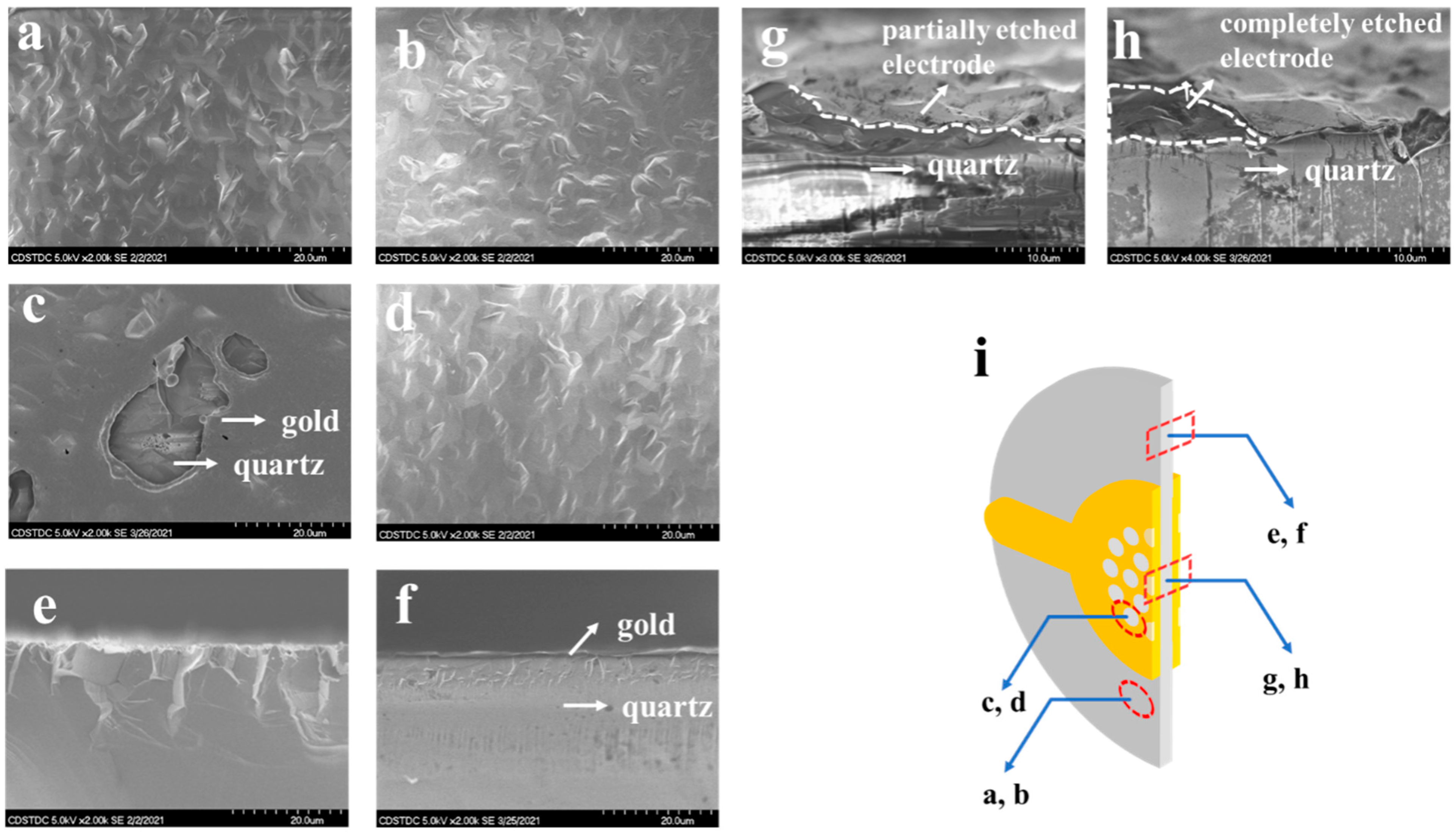
3.2. Morphology Analysis
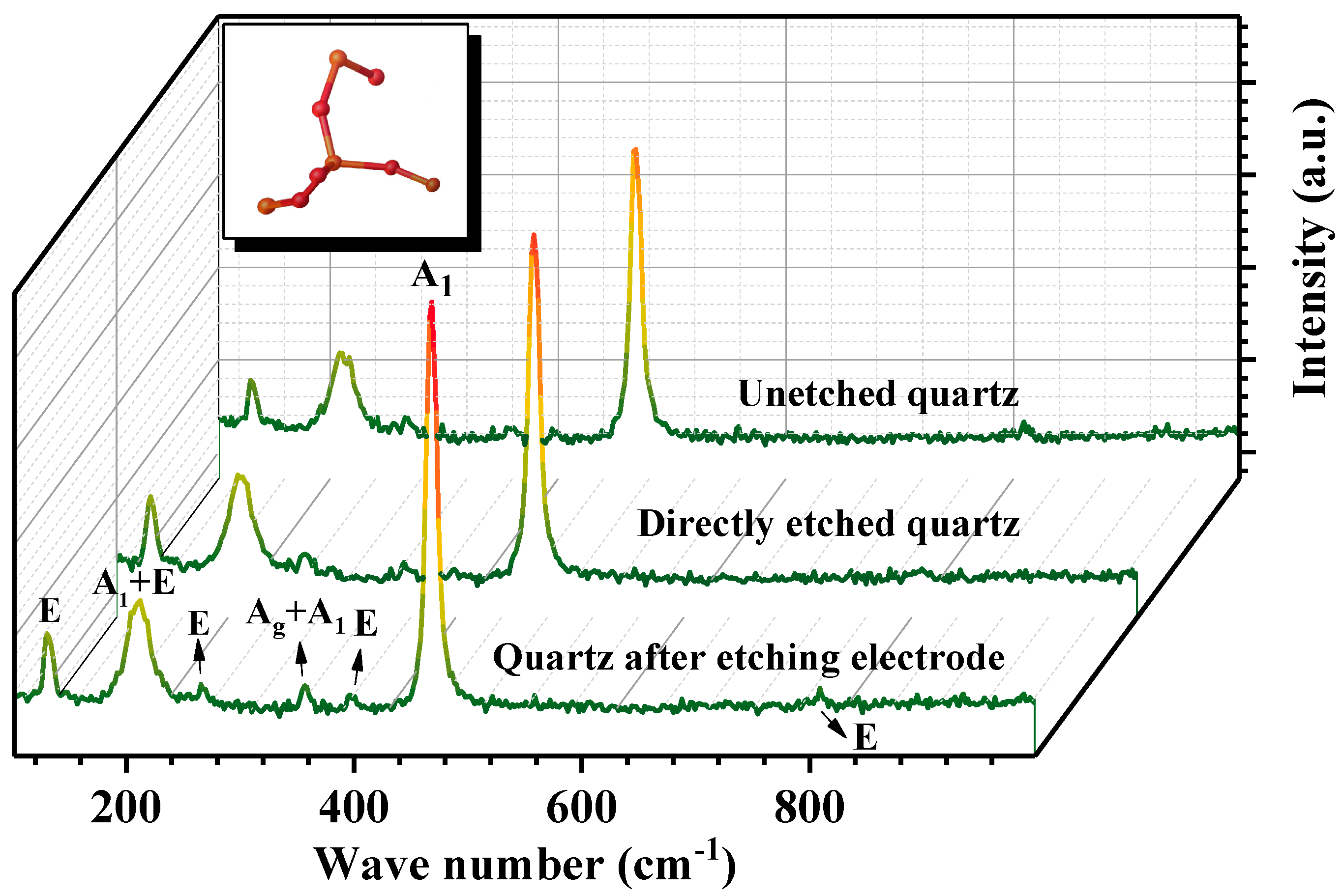
3.3. Raman Spectra
4. Conclusions
Author Contributions
Funding
Acknowledgments
Conflicts of Interest
References
- Bo, M.A.; Tian, W.; Zhao, Q.; Chen, F.; Lei, O.; Laboratory, S.K. Researchon Force Sensitivity and Stability of Multi-electrode Quartz Force Sensitive Resonator. Piezoelectrics Acoustooptics 2017, 39, 865–868. [Google Scholar]
- Wu, G.Q.; Xu, J.H.; Ng, E.J.; Chen, W. MEMS Resonators for Frequency Reference and Timing Applications. J. Microelectromech. Syst. 2020, 29, 1137–1166. [Google Scholar] [CrossRef]
- Li, H.; Chen, X.D.; Zhao, J. Dynamic Analysis of AT-Cut Quartz Crystal Resonators with FEM Method. J. Synth. Cryst. 2017, 46, 782–785. [Google Scholar]
- Jing, J.; Meng, Z.; Ueda, T.; Ikezawa, S. Optimal design work for high-frequency quartz resonators. In Proceedings of the 2016 10th International Conference on Sensing Technology (ICST), Nanjing, China, 11–13 November 2016. [Google Scholar]
- Pei, J.-Y.; Ma, T.-F.; Wu, R.-X.; Huang, B.; Wang, J.; Jian-Ke, D.U. Quartz resonators operating with slow shear modes driven by lateral electric fields produced by surface electrodes. In Proceedings of the 2016 Symposium on Piezoelectricity, Acoustic Waves, and Device Applications (SPAWDA), Xi’an, China, 21–24 October 2016; Institute of Electrical and Electronics Engineers (IEEE): New York, NY, USA; pp. 145–149. [Google Scholar]
- Shiono, T.; Osada, Y.; Nakagawa, Y. Frequency Change of Quartz Crystal Resonator Caused during Ion Beam Etching. Jpn. J. Appl. Phys. 2007, 46, 4647–4651. [Google Scholar] [CrossRef]
- Chang, D.T.; Yoon, Y.; Moyer, H.P.; Brewer, P.D.; Nguyen, H.D. Ultra-miniature fundamental-mode UHF quartz MEMS oscil-lator. In Proceedings of the 2017 19th International Conference on Solid-State Sensors, Actuators and Microsystems (TRANS-DUCERS), Kaohsiung, Taiwan, 18–22 June 2017; pp. 187–190. [Google Scholar] [CrossRef]
- Li, B.; Li, C.; Zhao, Y.L.; Han, C.; Zhang, Q.W. Deep Reactive Ion Etching of Z-Cut Alpha Quartz for MEMS Resonant Devices Fabrication. Micromachines 2020, 11, 724. [Google Scholar] [CrossRef]
- Joseph, A.; Emadi, A. A High Frequency Dual Inverted Mesa QCM Sensor Array with Concentric Electrodes. IEEE Access 2020, 8, 92669–92676. [Google Scholar] [CrossRef]
- Raicheva, Z.; Georgieva, V.; Grechnikov, A.; Gadjanova, V.; Angelov, T.; Vergov, L.; Lazarov, Y. Improving Resonance Char-acteristics of Gas Sensors by Chemical Etching of Quartz Plates. In Proceedings of the 17th International School on Condensed Matter Physics, Varna, Bulgaria, 2–7 September 2012; Iop Publishing Ltd: Bristol, UK, 2012; Volume 398. [Google Scholar]
- Wellershoff, S.-S.; Hohlfeld, J.; Gudde, J.; Matthias, E. The role of electron-phonon coupling in femtosecond laser damage of metals. Appl. Phys. A Mater Sci. Process 1999, 69, S99–S107. [Google Scholar] [CrossRef]
- Hohlfeld, J.; Wellershoff, S.-S.; Gudde, J.; Conrad, U.; Jahnke, V.; Matthias, E. Electron and lattice dynamics following optical excitation of metals. Chem. Phys. 2000, 251, 237–258. [Google Scholar] [CrossRef]
- Hohlfeld, J.; Muller, J.G.; Wellershoff, S.-S.; Matthias, E. Time-resolved thermoreflectivity of thin gold films and its dependence on film thickness. Appl. Phys. B Lasers Opt. A 1997, 64, 387–390. [Google Scholar] [CrossRef]
- Venkatakrishnan, K.; Tan, B.; Ngoi, B. Femtosecond pulsed laser ablation of thin gold film. Opt. Laser Technol. 2002, 34, 199–202. [Google Scholar] [CrossRef]
- Kamlage, G.; Bauer, T.; Ostendorf, A.; Chichkov, B.K.A. Deep drilling of metals by femtosecond laser pulses. Appl. Phys. A 2003, 77, 307–310. [Google Scholar] [CrossRef]
- Gamaly, E.G.; Luther-Davies, B.; Kolev, V.Z.; Madsen, N.R.; Duering, M.; Rode, A.V. Ablation of metals with picosecond laser pulses: Evidence of long-lived non-equilibrium surface states. Laser Part. Beams 2005, 23, 167–176. [Google Scholar] [CrossRef]
- Gamaly, E.G.; Rode, A.V.; Luther-Davies, B.; Tikhonchuk, V.T. Ablation of solids by femtosecond lasers: Ablation mechanism and ablation thresholds for metals and dielectrics. Phys. Plasmas 2002, 9, 949–957. [Google Scholar] [CrossRef]
- Jiang, L.; Tsai, H.-L. Improved Two-Temperature Model and Its Application in Ultrashort Laser Heating of Metal Films. J. Heat Transf. Trans. ASME 2005, 127, 1167–1173. [Google Scholar] [CrossRef] [Green Version]
- Shao, J.; Wang, D.; Ren, G. Laser Thinning and Trimming of Films in Vacuum. Chinese Journal of Vacuum Sci. Technol. 2008, S1, 93–97. [Google Scholar]
- Bottom, V.E. Introduction to Quartz Crystal Unit Design; Van Nostrand Reinhold: New York, NY, USA, 1982. [Google Scholar]
- Bennett, T.D.; Grigoropoulos, C.; Krajnovich, D.J. Near-threshold laser sputtering of gold. J. Appl. Phys. 1995, 77, 849–864. [Google Scholar] [CrossRef]
- Garrison, B.J.; Itina, T.E.; Zhigilei, L.V. Limit of overheating and the threshold behavior in laser ablation. Phys. Rev. E 2003, 68, 041501. [Google Scholar] [CrossRef] [Green Version]
- Boyer, H.; Smith, D.C.; Chopin, C.; Lasnier, B. Raman Microprobe (Rmp) Determinations of Natural and Synthetic Coesite. Phys. Chem. Miner. 1985, 12, 45–48. [Google Scholar]
- Scott, J.F.; Porto, S.P.S. Longitudinal and Transverse Optical lattice Vibrations in Quartz. Phys. Rev. 1967, 161, 903–910. [Google Scholar] [CrossRef]
- Sharma, S.K.; Mammone, J.F.; Nicol, M.F. Raman investigation of ring configurations in vitreous silica. Nat. Cell Biol. 1981, 292, 140–141. [Google Scholar] [CrossRef]
- Tekippe, V.J.; Ramdas, A.K.; Rodriguez, S. Piezospectroscopic Study of the Raman Spectrum ofα-Quartz. Phys. Rev. B 1973, 8, 706–717. [Google Scholar] [CrossRef]


| Status | F (Hz) | C0 (pF) | RR (ohms) | Q (k) | C1 (fF) | L (mH) | |
|---|---|---|---|---|---|---|---|
| Type a | Before Etching | 10,000,015 | 5.9237 | 17.7431 | 32 | 28.4628 | 8.8994 |
| After Etching | 10,000,027 | 5.8277 | 18.9616 | 30 | 28.1305 | 9.0045 | |
| Type b | Before Etching | 10,008,240 | 3.2577 | 18.005 | 60 | 14.6945 | 17.2095 |
| After Etching | 10,012,369 | 3.2095 | 507.9951 | 2 | 14.5876 | 17.3214 | |
| Type c | Before Etching | 10,011,762 | 3.2757 | 17.358 | 63 | 14.57 | 17.3444 |
| After Etching | 10,018,391 | 3.1095 | 855.5109 | 1 | 12.8702 | 19.6091 |
Publisher’s Note: MDPI stays neutral with regard to jurisdictional claims in published maps and institutional affiliations. |
© 2021 by the authors. Licensee MDPI, Basel, Switzerland. This article is an open access article distributed under the terms and conditions of the Creative Commons Attribution (CC BY) license (https://creativecommons.org/licenses/by/4.0/).
Share and Cite
Zhang, J.-L.; Liao, S.; Chen, C.; Yang, X.-T.; Lin, S.-A.; Tan, F.; Li, B.; Wang, W.-W.; Zhong, Z.-X.; Zeng, G.-G. Research on Trimming Frequency-Increasing Technology for Quartz Crystal Resonator Using Laser Etching. Micromachines 2021, 12, 894. https://doi.org/10.3390/mi12080894
Zhang J-L, Liao S, Chen C, Yang X-T, Lin S-A, Tan F, Li B, Wang W-W, Zhong Z-X, Zeng G-G. Research on Trimming Frequency-Increasing Technology for Quartz Crystal Resonator Using Laser Etching. Micromachines. 2021; 12(8):894. https://doi.org/10.3390/mi12080894
Chicago/Turabian StyleZhang, Jun-Lin, Shuang Liao, Cheng Chen, Xiu-Tao Yang, Sheng-Ao Lin, Feng Tan, Bing Li, Wen-Wu Wang, Zheng-Xiang Zhong, and Guang-Gen Zeng. 2021. "Research on Trimming Frequency-Increasing Technology for Quartz Crystal Resonator Using Laser Etching" Micromachines 12, no. 8: 894. https://doi.org/10.3390/mi12080894