
Double-Quantum-Well AlGaN/GaN Field Effect Transistors with Top and Back Gates: Electrical and Noise Characteristics

 ,
,  , , ,
, , ,  , , , and
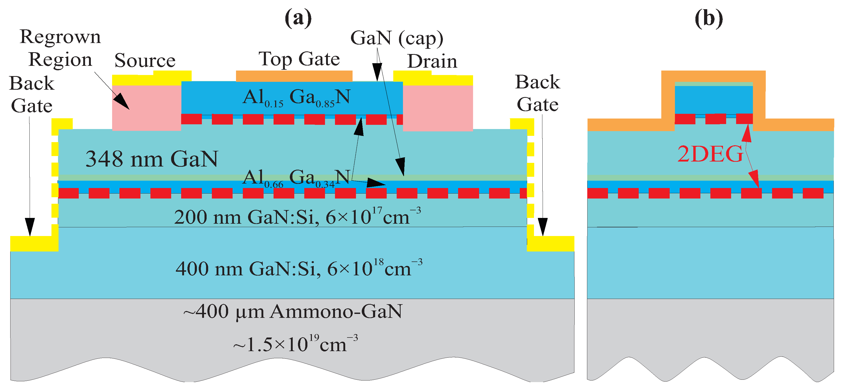
Abstract
:1. Introduction
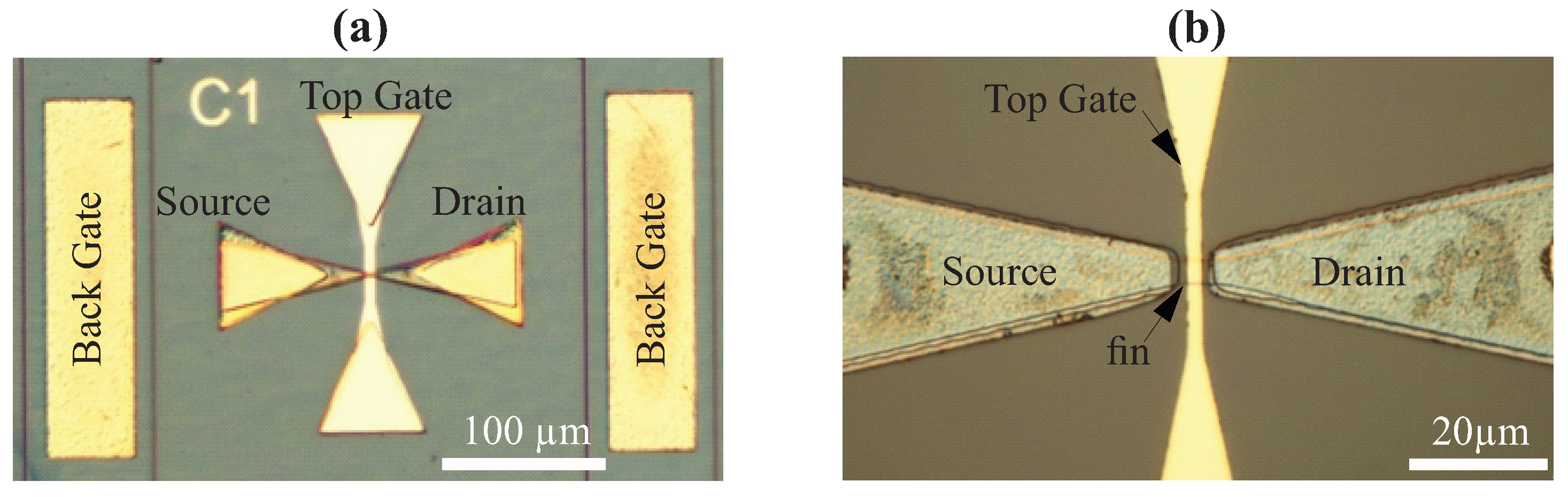
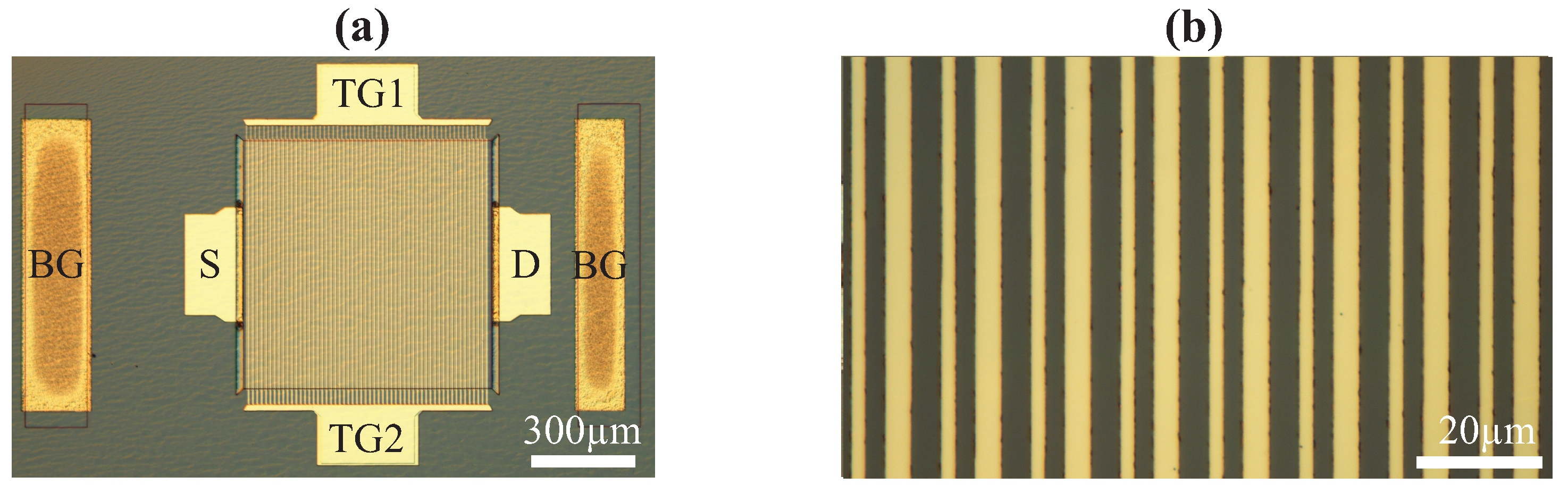
2. Device Fabrication and Experimental Details
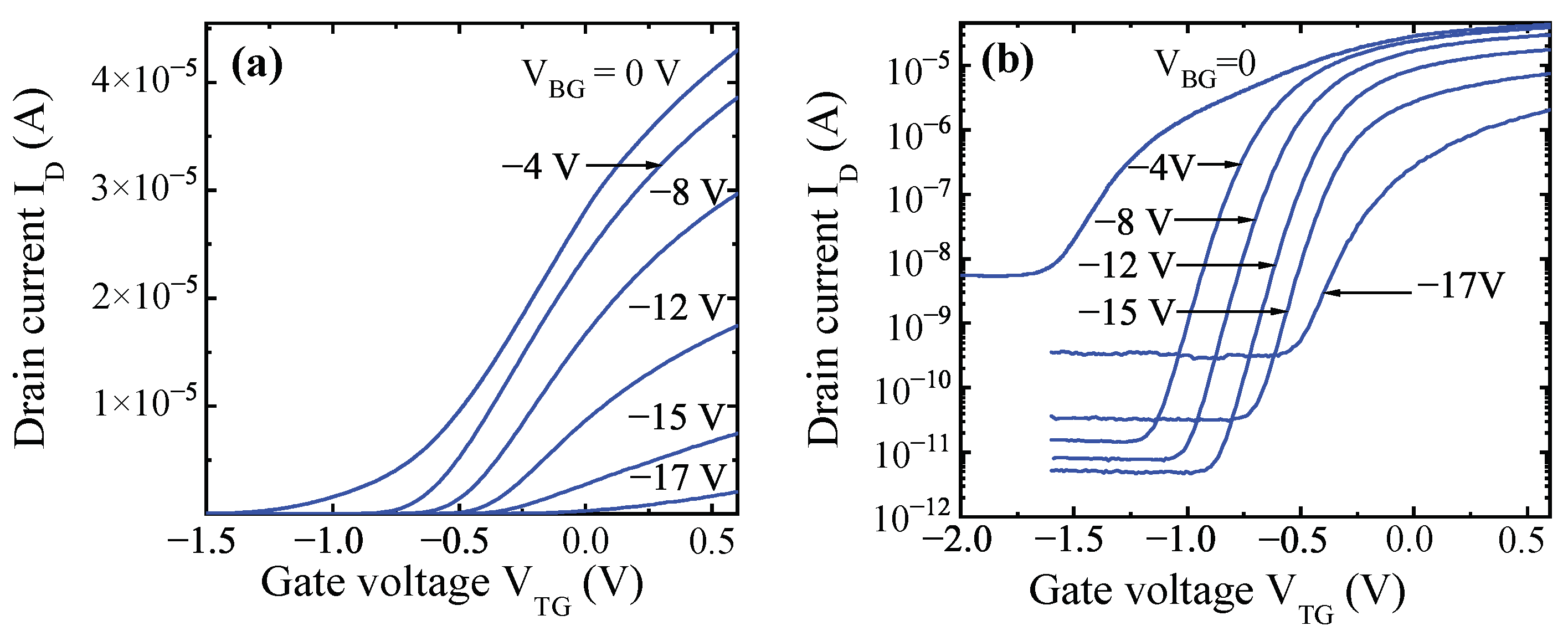
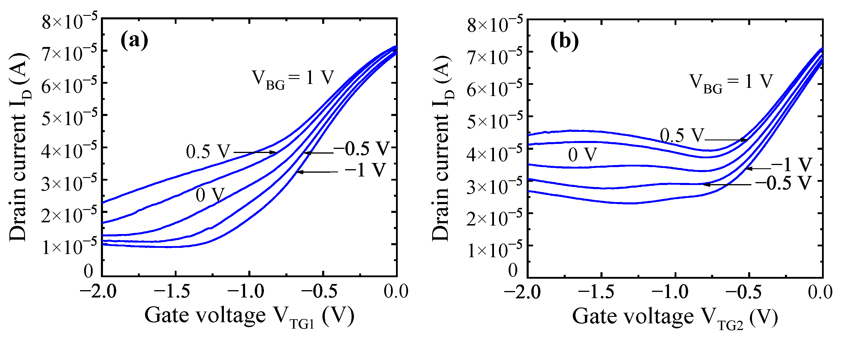
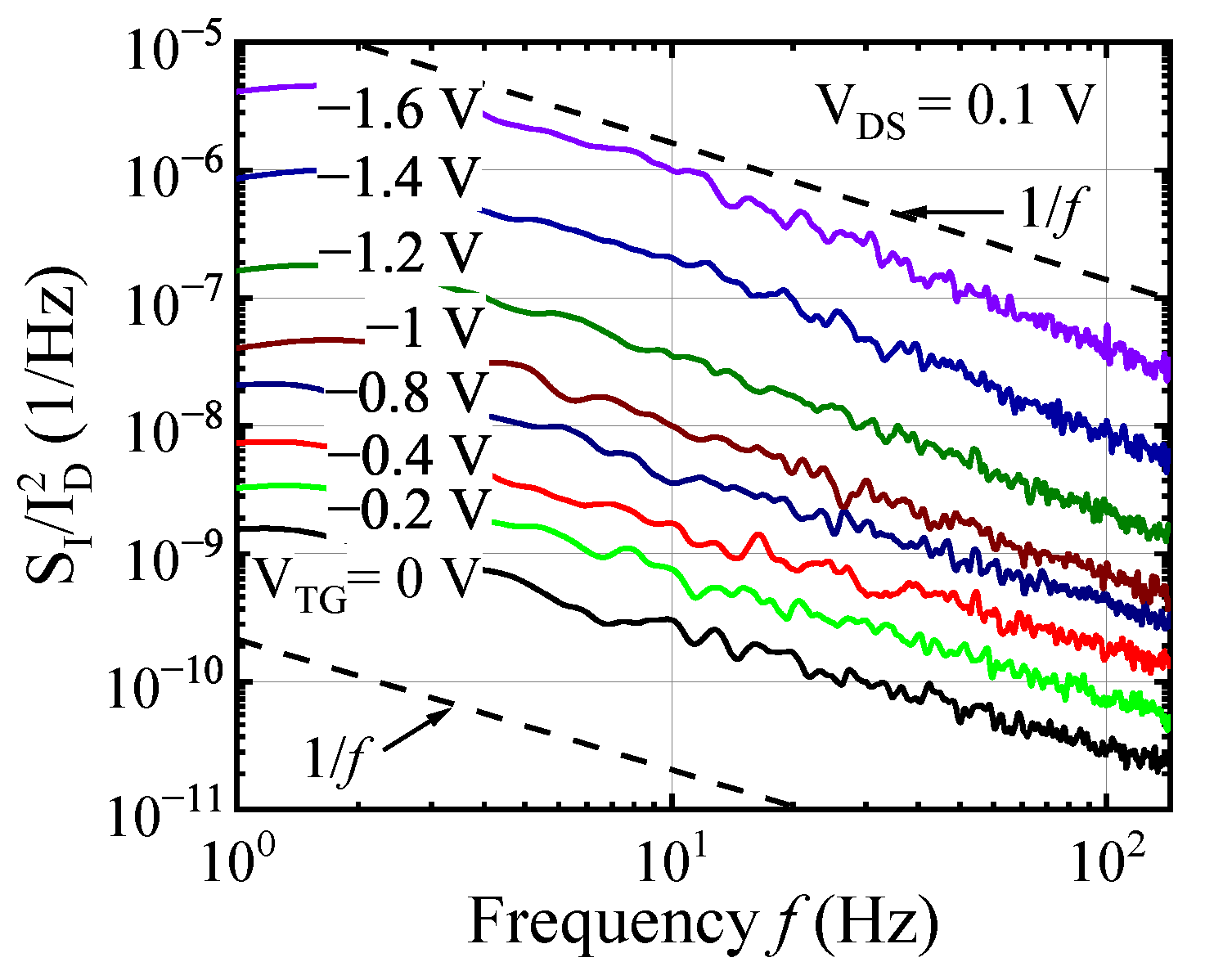
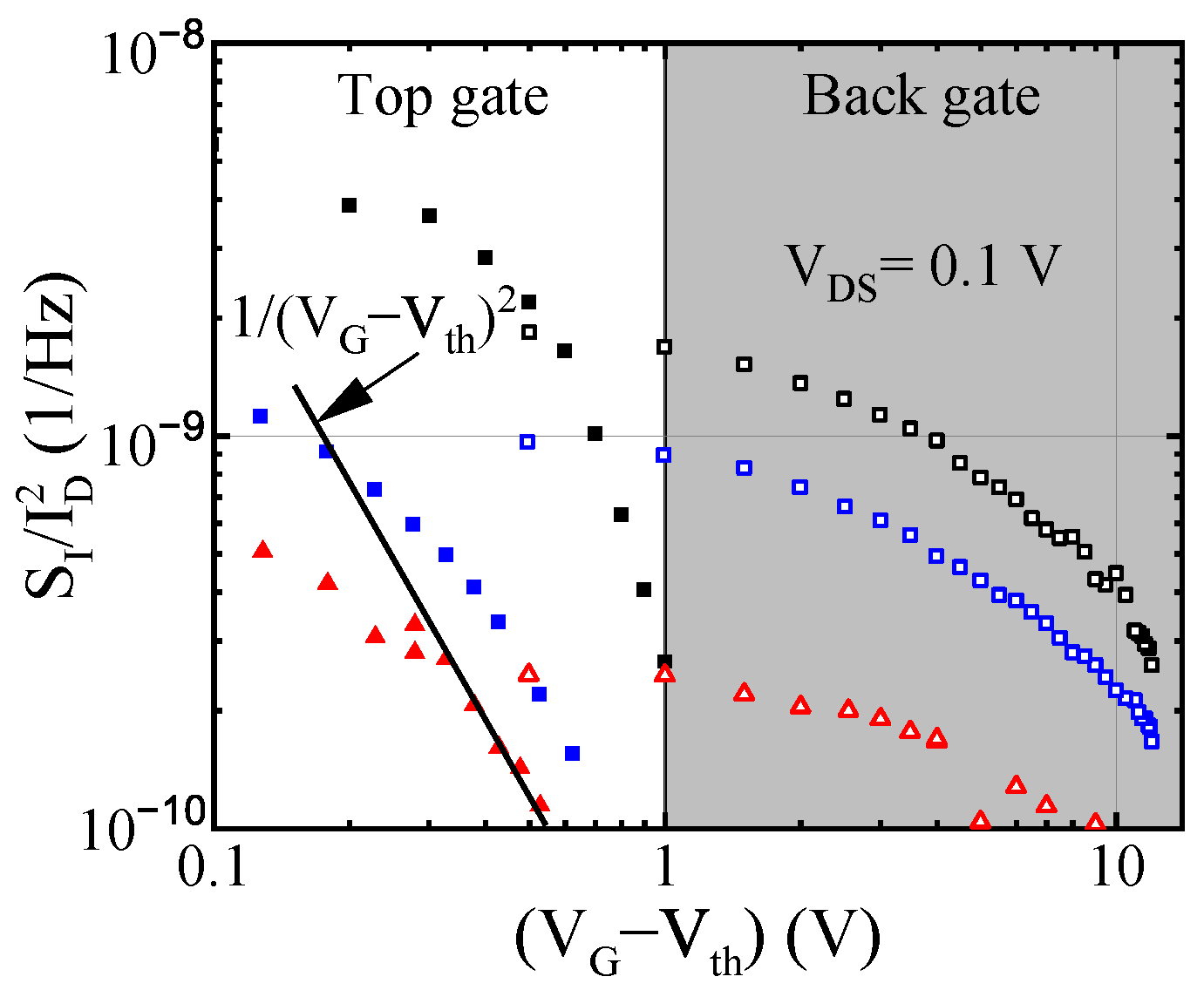
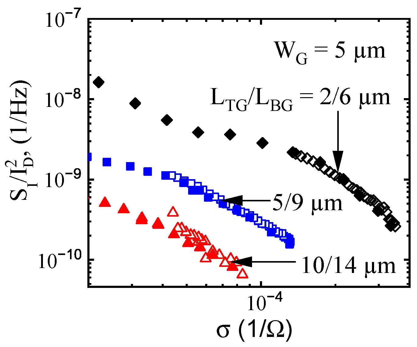
3. Results and Discussion
4. Conclusions
Author Contributions
Funding
Conflicts of Interest
Abbreviations
| HEMT | High Electron Mobility Transistor |
| FinHEMT | Fin-Shaped High Electron Mobility Transistor |
| MOSFET | Metal-Oxide-Semiconductor Field-Effect Transistor |
References
- Nahhas, A.M. Review of AlGaN/GaN HEMTs based devices. Am. J. Nanomater. 2019, 7, 10–21. [Google Scholar]
- Zeng, F.; An, X.J.; Zhou, G.; Li, W.; Wang, H.; Duan, T.; Jiang, L.; Yu, H. A comprehensive review of recent progress on GaN high electron mobility transistors: Devices, fabrication and reliability. Electronics 2018, 7, 377. [Google Scholar] [CrossRef] [Green Version]
- Khan, M.A.; Van Hove, J.M.; Kuznia, J.N.; Olson, D.T. High electron mobility GaN/AlxGa1−xN heterostructures grown by low-pressure metalorganic chemical vapor deposition. Appl. Phys. Lett. 1991, 58, 2408–2410. [Google Scholar] [CrossRef]
- Asif, K.M.; Bhattarai, A.; Kuznia, J.N.; Olson, D.T. High electron mobility transistor based on a GaN-AlxGa1−xN heterojunction. Appl. Phys. Lett. 1993, 63, 1214–1215. [Google Scholar] [CrossRef]
- Gaska, R.; Shur, M.S.; Fjeldly, T.A.; Bykhovski, A.D. Two-channel AlGaN/GaN heterostructure field effect transistor for high power applications. Appl. Phys. 1999, 85, 3009–3011. [Google Scholar] [CrossRef]
- Heikman, S.S.; Keller, S.; Green, D.S.; DenBaars, S.P.; Mishra, U.K. High conductivity modulation doped AlGaN/GaN multiple channel heterostructures. J. Appl. Phys. 2003, 94, 5321–5325. [Google Scholar] [CrossRef]
- Wille, A.; Yacoub, H.; Debald, A.; Kalisch, H.; Vescan, A. AlGaN/AlN-GaN-SL HEMTs with multiple 2DEG channels. J. Electron. Mater. 2015, 44, 1263–1267. [Google Scholar] [CrossRef]
- Xue, J.S.; Zhang, J.; Zhang, K.; Zhao, Y.; Zhang, L.; Ma, X.; Li, X.; Meng, F.; Hao, Y. Fabrication and characterization of InAlN/GaN-based double-channel high electron mobility transistors for electronic applications. J. Appl. Phys. 2012, 111, 114513. [Google Scholar] [CrossRef] [Green Version]
- Meng, F.; Zhang, J.; Zhou, H.; Ma, J.; Xue, J.; Dang, L.; Zhang, L.; Lu, M.; Ai, S.; Li, X.; et al. Transport characteristics of AlGaN/GaN/AlGaN double heterostructures with high electron mobility. J. Appl. Phys. 2012, 112, 023707. [Google Scholar] [CrossRef]
- Chu, R.; Zhou, Y.; Liu, J.; Wang, D.; Chen, K.J.; Lau, K.M. AlGaN-GaN double-channel HEMTs. IEEE Trans. Electron. Devices 2005, 52, 438–446. [Google Scholar] [CrossRef]
- Kamath, A.; Patil, T.; Adari, R.; Bhattacharya, I.; Ganguly, S.; Aldhaheri, R.W.; Hussain, M.A.; Saha, D. Double-channel AlGaN/GaN high electron mobility transistor with back barriers. IEEE Electron Device Lett. 2012, 33, 1690–1692. [Google Scholar] [CrossRef]
- Kuzmík, J.; Blaho, M.; Pogány, D.; Gornik, E.; Alam, A.; Dikme, Y.; Heuken, M.; Javorka, P.; Kordos, P. Backgating, high-current and breakdown characterisation of AlGaN/GaN HEMTs on silicon substrates. IEEE Electron Device Lett. 2012, 33. [Google Scholar]
- Wang, L.; Zhang, X.; You, G.; Xiong, F.; Liang, L.; Hu, Y.; Chen, A.; Liu, J.; Xu, J. Modeling the back gate effects of AlGaN/GaN HEMTs. J. Comput. Electron. 2012, 13, 872–876. [Google Scholar] [CrossRef]
- Hwang, Y.H.; Dong, C.; Hsieh, Y.L.; Zhu, W.; Ahn, S.; Ren, F.; Pearton, S.J.; Kravchenko, I.I. Improvement of drain breakdown voltage with a back-side gate on AlGaN/GaN high electron mobility transistors. J. Vac. Sci. Technol. B 2015, 33, 042201. [Google Scholar] [CrossRef]
- Gupta, C.; Gupta, A.; Bansal, A.; Dixit, A. Suppression of short-channel effects by double-gate double-channel device design in normally-off AlGaN/GaN MIS-HEMTs. IETE J. Res. 2018, 1–8. [Google Scholar] [CrossRef]
- Chen, D.; Liu, Z.; Liang, J.; Wan, L.; Xie, Z.; Li, G. A sandwich-structured AlGaN/GaN HEMT with broad transconductance and high breakdown voltage. J. Mater. Chem. C 2019, 39, 12075–12079. [Google Scholar] [CrossRef]
- Lin, W.T.; Liao, W.C.; Zhong, Y.N.; Hsin, Y.M. AlGaN/GaN HEMTs with 2DHG back gate control. MRS Adv. 2018, 3, 137–141. [Google Scholar] [CrossRef]
- Lin, W.T.; Lin, W.C.; Zhong, Y.N.; Hsin, Y.M. AlGaN/GaN high electron mobility transistors with a p-GaN backgate structure. ECS Trans. 2018, 85, 49. [Google Scholar] [CrossRef]
- Peralta, X.G.; Allen, S.J.; Wanke, M.C.; Harff, N.E.; Simmons, J.A.; Lilly, M.P.; Reno, J.L.; Burke, P.J.; Eisenstein, J.P. Terahertz photoconductivity and plasmon modes in double-quantum-well field-effect transistors. Appl. Phys. Lett. 2002, 81, 1627–1629. [Google Scholar] [CrossRef] [Green Version]
- Wang, L.; Chen, X.S.; Hu, W.D.; Wang, J.; Wang, J.; Wang, X.D.; Lu, W. The plasmonic resonant absorption in GaN double-channel high electron mobility transistors. Appl. Phys. Lett. 2011, 99, 063502. [Google Scholar] [CrossRef] [Green Version]
- Caddemi, A.; Boglione, L.; Cardillo, E.; Crupi, G.; Roussos, J.A. Cross-Laboratory Experimental Validation of a Tunerless Technique for the Microwave Noise Parameters Extraction. IEEE Trans. Microw. Theory Tech. 2021, 69, 1733–1739. [Google Scholar] [CrossRef]
- Caddemi, A.; Cardillo, E.; Salvo, G.; Petane, S. Microwave effects of UV light exposure of a GaN HEMT: Measurements and model extraction. Microelectron. Reliab. 2016, 65, 310–317. [Google Scholar] [CrossRef]
- Wang, Y.; Dai, W.; Wu, Y.; Guo, Y.; Xu, R.; Yan, B.; Xu, Y. A bendable microwave GaN HEMT on CVD Parylene-C substrate. In Proceedings of the 2020 IEEE MTT-S International Conference on Numerical Electromagnetic and Multiphysics Modeling and Optimization (NEMO), Hangzhou, China, 7–9 December 2020; Volume 65, pp. 1–4. [Google Scholar]
- Wang, Y.; Wu, Q.; Mao, S.; Xu, R.; Yan, B.; Xu, Y. Bendable Microwave AlGaN/GaN High-Electron-Mobility Transistor With Output Power Density of 2.65 W/mm. IEEE Electron. Device Lett. 2021, 42, 677–680. [Google Scholar] [CrossRef]
- Nagarajan, V.; Chen, K.M.; Lim, H.Y.; Hu, H.H.; Huang, G.W.; Lin, C.J.; Chen, B.Y.; Anandan, D.; Singh, S.K.; Wu, C.H.; et al. Low-Frequency Noise Characterization of AlGaN/GaN HEMTs and MIS-HEMTs Under UV Illumination. IEEE Trans. Nanotechnol. 2020, 19, 405–409. [Google Scholar] [CrossRef]
- Chiu, H.C.; Peng, L.Y.; Yang, C.W.; Wang, H.C.; Hsin, Y.M.; Chyi, J.I. Analysis of the back-gate effect in normally OFF p-GaN gate high-electron mobility transistor. IEEE Trans. Electron. Devices 2015, 62, 507–511. [Google Scholar] [CrossRef]
- Wojtasiak, W.; Góralczyk, M.; Gryglewski, D.; Zając, M.; Kucharski, R.; Prystawko, P.; Piotrowska, A.; Ekieiski, M.; Kamińska, E.; Taube, A.; et al. AlGan/GaN high electron mobility transistors on semi-insulating ammono-GaN substrates with regrown ohmic contacts. Micromachines 2018, 9, 546. [Google Scholar] [CrossRef] [Green Version]
- Popov, V.V.; Fateev, D.V.; Otsuji, T.; Meziani, Y.M.; Coquillat, D.; Knap, W. Plasmonic terahertz detection by a double-grating-gate field-effect transistor structure with an asymmetric unit cell. Appl. Phys. Lett. 2011, 99, 243504. [Google Scholar] [CrossRef] [Green Version]
- Watanabe, T.; Tombet, S.B.; Tanimoto, Y.; Wang, Y.; Minamide, H.; Ito, H.; Feteev, D.; Popov, V.; Coquillat, D.; Knap, W.; et al. Ultrahigh sensitive plasmonic terahertz detector based on an asymmetric dual-grating gate HEMT structure. Solid-State Electron. 2012, 78, 109–114. [Google Scholar] [CrossRef]
- Wang, L.; Chen, X.; Hu, W.; Yu, A.; Lu, W. The resonant tunability, enhancement, and damping of plasma waves in the two-dimensional electron gas plasmonic crystals at terahertz frequencies. Appl. Phys. Lett. 2013, 102, 243507. [Google Scholar] [CrossRef]
- Shalygin, V.A.; Moldavskaya, M.D.; Vinnichenko, M.Y.; Maremyanin, K.V.; Artemyev, A.A.; Panevin, V.Y.; Vorobjev, L.E.; Firsov, D.A.; Korotyeyev, V.V.; Sakharov, A.V.; et al. Selective terahertz emission due to electrically excited 2D plasmons in AlGaN/GaN heterostructure. J. Appl. Phys. 2019, 126, 183104. [Google Scholar] [CrossRef]
- Hubmann, S.; Bel’kov, V.V.; Golub, L.E.; Kachorovskii, V.Y.; Drienovsky, M.; Eroms, J.; Weiss, D.; Ganichev, S.D. Giant ratchet magneto-photocurrent in graphene lateral superlattices. Phys. Rev. Res. 2020, 2, 033186. [Google Scholar] [CrossRef]
- Sai, P.; Potashin, S.O.; Szola, M.; Yavorskiy, D.; Cywinski, G.; Prystawko, P.; Lusakowski, J.; Ganichev, S.D.; Rumyantsev, S.; Knap, W.; et al. Beatings of ratchet current magneto-oscillations in GaN-based grating gate structures: Manifestation of spin-orbit band splitting. Phys. Rev. B 2021. accepted for publication. [Google Scholar]
- Birner, S.; Zibold, T.; Andlauer, T.; Kubis, T.; Sabathil, M.; Trellakis, A.; Vogl, P. Nextnano: General purpose 3-D simulations. IEEE Trans. Electron. Devices 2007, 54, 2137–2142. [Google Scholar] [CrossRef]
- Sai, P.; Jorudas, J.; Dub, M.; Sakowicz, M.; Jakštas, V.; But, D.B.; Prystawko, P.; Cywinski, G.; Kašalynas, I.; Knap, W.; et al. Low frequency noise and trap density in GaN/AlGaN field effect transistors. Appl. Phys. Lett. 2019, 115, 183501. [Google Scholar] [CrossRef]
- Im, K.S.; Reddy, M.S.P.; Caulmilone, R.; Theodorou, C.G.; Ghibaudo, G.; Cristoloveanu, S.; Lee, J.H. Low-frequency noise characteristics of GaN nanowire gate-all-around transistors with/without 2-DEG channel. IEEE Trans. Electron. Devices 2019, 66, 1243–1248. [Google Scholar] [CrossRef]
- Handler, P.; Farnsworth, H.E.; Kleiner, W.H.; Law, J.T.; Garrett, C.G.B.; Autler, H.; McWhorter, A.L. Electrical Properties of a Clean Germanium Surface. In Semiconductor Surface Physics; Kingston, R.H., Ed.; University of Pennsylvania Press: Philadelphia, PA, USA, 1957; pp. 23–52. [Google Scholar]
- Christensson, S.; Lundström, I.; Svensson, C. Low frequency noise in MOS transistors—I theory. Solid-State Electron. 1968, 66, 797–812. [Google Scholar] [CrossRef]
- Dmitriev, A.P.; Levinshtein, M.E.; Rumyantsev, S.L. On the Hooge relation in semiconductors and metals. J. Appl. Phys. 2009, 103, 024514. [Google Scholar] [CrossRef]
- Takakura, K.; Putcha, V.; Simoen, E.; Alian, A.R.; Peralagu, U.; Waldron, N.; Parvais, B.; Collaert, N. Low-Frequency Noise Investigation of GaN/AlGaN Metal–Oxide–Semiconductor High-Electron-Mobility Field-Effect Transistor with Different Gate Length and Orientation. IEEE Trans. Electron. Devices 2020, 67, 3062–3068. [Google Scholar] [CrossRef]
- Choi, Y.J.; Lee, J.H.; An, S.J.; Im, K.S. Low-Frequency Noise Behavior of AlGaN/GaN HEMTs with Different Al Compositions. Crystals 2020, 10, 830. [Google Scholar] [CrossRef]
- Dub, M.; Sai, P.; Przewłoka, A.; Krajewska, A.; Sakowicz, M.; Prystawko, P.; Kasperski, J.; Pasternak, I.; Cywiński, G.; But, D.; et al. Graphene as a Schottky Barrier Contact to AlGaN/GaN Heterostructures. Materials 2020, 13, 4140. [Google Scholar] [CrossRef]
- Chiu, H.C.; Yang, C.W.; Chen, C.H.; Wu, C.H. Quality of the oxidation interface of AlGaN in enhancement-mode AlGaN/GaN high-electron mobility transistors. IEEE Trans. Electron. Devices 2012, 59, 3334–3338. [Google Scholar] [CrossRef]
- Jorudas, J.; Šimukovič, A.; Dub, M.; Sakowicz, M.; Prystawko, P.; Indrišiūnas, S.; Kovalevskij, V.; Rumyantsev, S.; Knap, W.; Kašalynas, I. AlGaN/GaN on SiC Devices without a GaN Buffer Layer: Electrical and Noise Characteristics. Micromachines 2020, 1, 1131. [Google Scholar] [CrossRef]


Publisher’s Note: MDPI stays neutral with regard to jurisdictional claims in published maps and institutional affiliations. |
© 2021 by the authors. Licensee MDPI, Basel, Switzerland. This article is an open access article distributed under the terms and conditions of the Creative Commons Attribution (CC BY) license (https://creativecommons.org/licenses/by/4.0/).
Share and Cite
Dub, M.; Sai, P.; Sakowicz, M.; Janicki, L.; But, D.B.; Prystawko, P.; Cywiński, G.; Knap, W.; Rumyantsev, S. Double-Quantum-Well AlGaN/GaN Field Effect Transistors with Top and Back Gates: Electrical and Noise Characteristics. Micromachines 2021, 12, 721. https://doi.org/10.3390/mi12060721
Dub M, Sai P, Sakowicz M, Janicki L, But DB, Prystawko P, Cywiński G, Knap W, Rumyantsev S. Double-Quantum-Well AlGaN/GaN Field Effect Transistors with Top and Back Gates: Electrical and Noise Characteristics. Micromachines. 2021; 12(6):721. https://doi.org/10.3390/mi12060721
Chicago/Turabian StyleDub, Maksym, Pavlo Sai, Maciej Sakowicz, Lukasz Janicki, Dmytro B. But, Paweł Prystawko, Grzegorz Cywiński, Wojciech Knap, and Sergey Rumyantsev. 2021. "Double-Quantum-Well AlGaN/GaN Field Effect Transistors with Top and Back Gates: Electrical and Noise Characteristics" Micromachines 12, no. 6: 721. https://doi.org/10.3390/mi12060721