
High-Accuracy Surface Topography Manufacturing for Continuous Phase Plates Using an Atmospheric Pressure Plasma Jet

Abstract
:1. Introduction
2. Experiment
2.1. Experiment Setup
2.2. APPJ Processing of Surface Topography
3. Methods
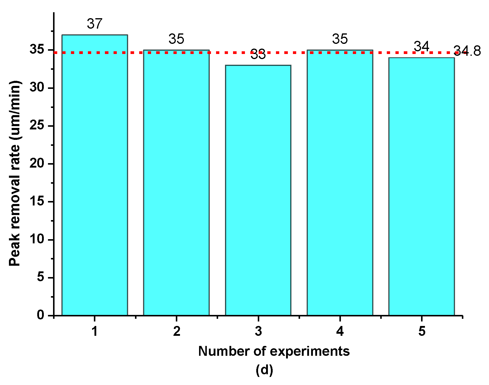
3.1. Removal Function
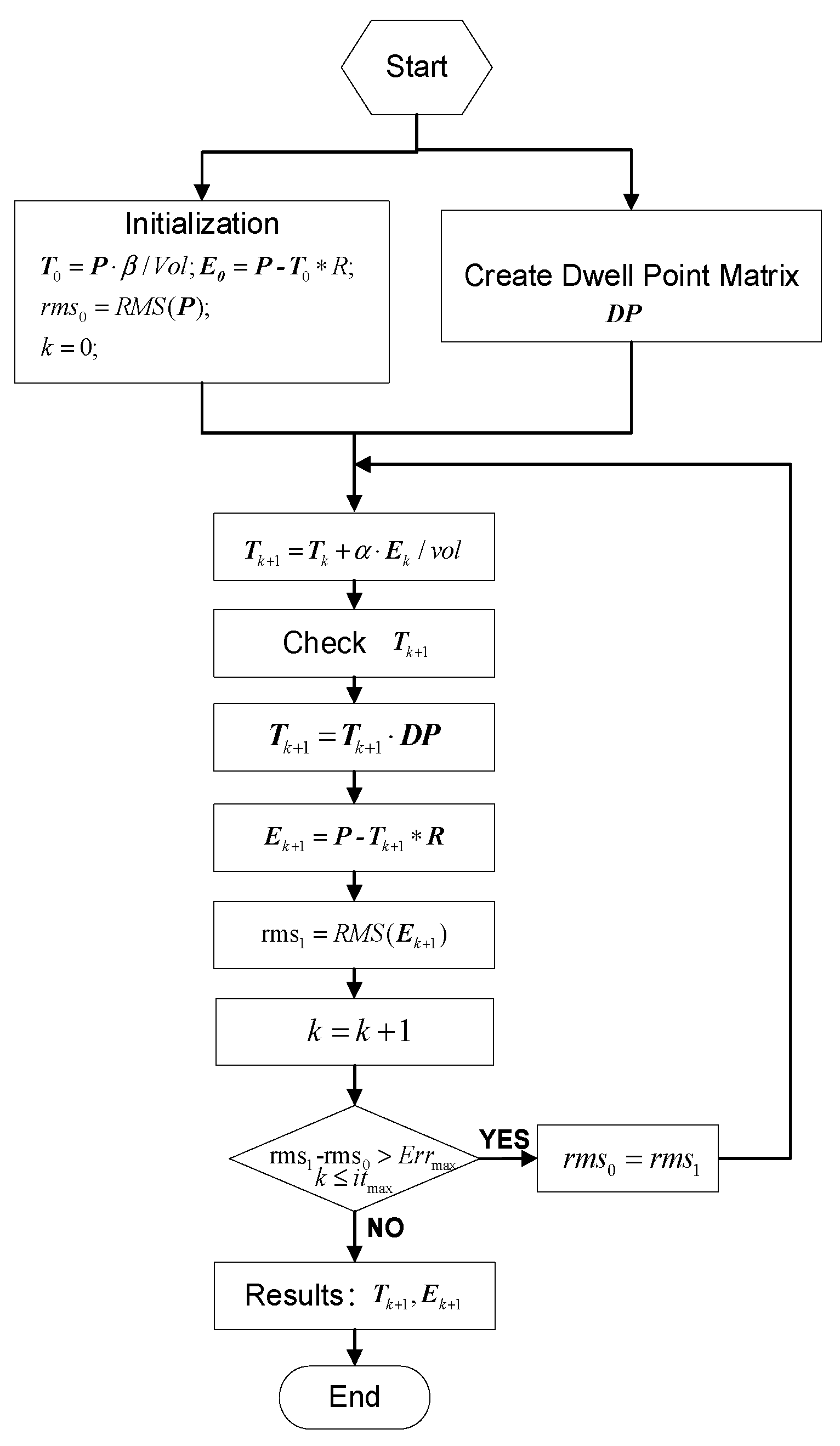
3.2. Dwell Time Algorithm
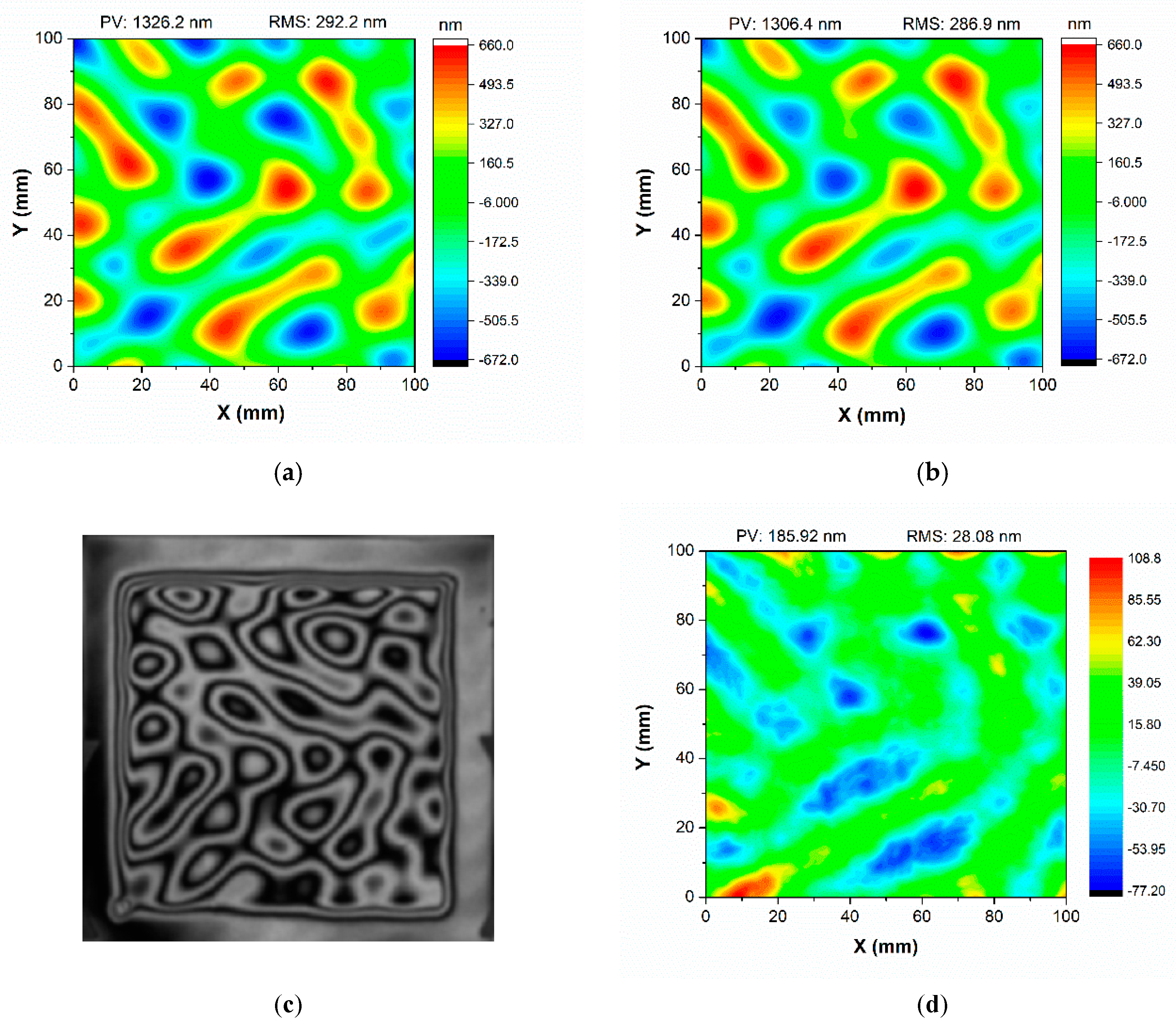
4. Results
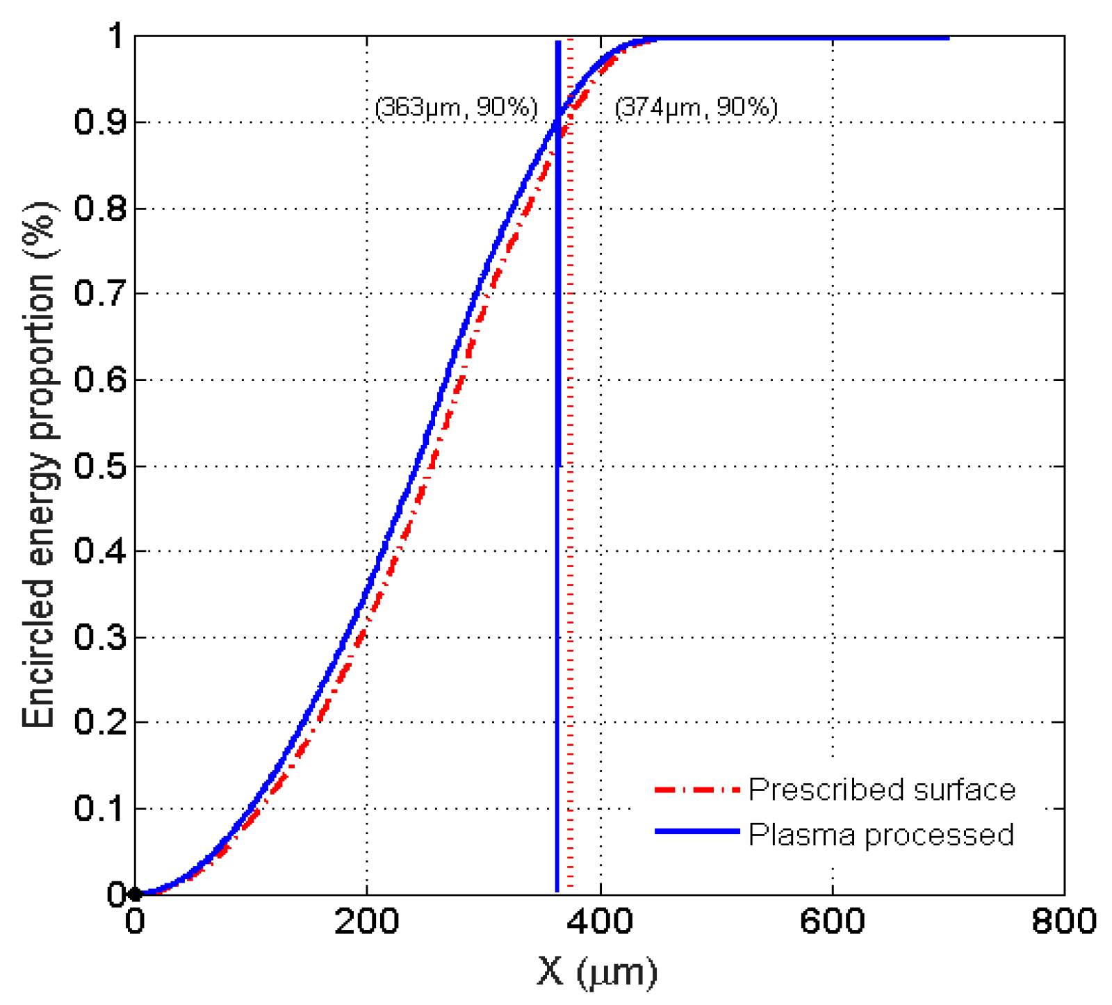
5. Discussion
6. Conclusions
Author Contributions
Funding
Acknowledgments
Conflicts of Interest
References
- Baisden, P.A.; Atherton, L.J.; Hawley, R.A.; Land, T.; Menapace, J.A.; Miller, P.E.; Runkel, M.J.; Spaeth, M.L.; Stolz, C.J.; Suratwala, T.I.; et al. Large Optics for the National Ignition Facility. Fusion Sci. Technol. 2016, 69, 295–351. [Google Scholar] [CrossRef]
- Moses, E.I.; Lindl, J.D.; Spaeth, M.L.; Patterson, R.W.; Sawicki, R.H.; Atherton, L.J.; Baisden, P.A.; Lagin, L.J.; Lar-son, D.W.; MacGowan, B.J.; et al. Overview: Development of the National Ignition Facility and the Transition to a User Facility for the Ignition Cam-paign and High Energy Density Scientific Research. Fusion Sci. Technol. 2016, 69, 1–24. [Google Scholar] [CrossRef]
- Yang, C.; Yan, H.; Wang, J.; Zhang, R. A novel design method for continuous-phase plate. Opt. Express 2013, 21, 11171–11180. [Google Scholar] [CrossRef]
- Hou, J.; Chen, X.H.; Li, J.; Zhong, B.; Deng, W.H. Processing technology of magnetorheological finishing for large-aperture optical components. In Proceedings of the Optical Design and Fabrication, OSA Technical Digest, Washington, DC, USA, 10–12 June 2019; p. JT5A.22. [Google Scholar]
- Menapace, J.A.; Davis, P.J.; Steele, W.A.; Hachkowski, M.R.; Nelson, A.; Xin, K. MRF applications: On the road to making large-aperture ultraviolet laser resistant continuous phase plates for high-power lasers. In Proceedings of the Boulder Damage Symposium XXXVIII: Annual Symposium on Optical Materials for High Power Lasers, Boulder, CO, USA, 25–27 September 2006; p. 64030N. [Google Scholar]
- Lindl, J.; Landen, O.; Edwards, J.D.M.; Moses, I.E.; NIC Team. Review of the National Ignition Campaign 2009–2012. Phys. Plasmas 2014, 21, 020501. [Google Scholar] [CrossRef]
- Menapace, J.A.; Ehrmann, P.E.; Bayramian, A.J.; Bullington, A.; Di Nicola, J.G.; Haefner, C.; Jarboe, J.; Marshall, C.; Schaffers, K.I.; Smith, C. Imprinting high-gradient topographical structures onto optical surfaces using magnetorheo-logical finishing: Manufacturing corrective optical elements for high-power laser applications. Appl. Opt. 2016, 55, 5240–5248. [Google Scholar] [CrossRef] [PubMed]
- Xu, M.; Dai, Y.; Xie, X.; Zhou, L.; Peng, W. Fabrication of continuous phase plates with small structures based on recursive frequency filtered ion beam figuring. Opt. Express 2017, 25, 10765. [Google Scholar] [CrossRef]
- Xu, M.; Dai, Y.F.; Xie, X.; Zhou, L.; Li, S.; Peng, W. Ion beam figuring of continuous phase plates based on the fre-quency filtering process. Front. Mech. Eng. 2017, 12, 110–115. [Google Scholar] [CrossRef]
- Jourdain, R.; Castelli, M.; Shore, P.; Sommer, P.; Proscia, D. Reactive atom plasma (RAP) figuring machine for meter class optical surfaces. Prod. Eng. 2013, 7, 665–673. [Google Scholar] [CrossRef] [Green Version]
- Yu, N.; Yang, Y.; Jourdain, R.; Gourma, M.; Bennett, A.; Fang, F. Design and optimization of plasma jet nozzles based on computational fluid dynamics. Int. J. Adv. Manuf. Tech. 2020, 108, 2559–2568. [Google Scholar] [CrossRef]
- Yang, X.; Kawai, K.; Arima, K.; Yamamura, K. Highly efficient planarization of sliced 4H–SiC (0001) wafer by slurry-less electrochemical mechanical polishing. Int. J. Mach. Tool Manuf. 2019, 144, 103431. [Google Scholar] [CrossRef]
- Sun, R.; Yang, X.; Watanabe, K.; Miyazaki, S.; Fukano, T.; Kitada, M.; Arima, K.; Kawai, K.; Yamamura, K. Etching Characteristics of Quartz Crystal Wafers Using Argon-Based Atmospheric Pressure CF4 Plasma Stabilized by Ethanol Addition. Nanomanuf. Metrol. 2019, 2, 168–176. [Google Scholar] [CrossRef]
- Arnold, T.; Böhm, G.; Fechner, R.; Meister, J.; Nickel, A.; Frost, F.; Hänsel, T.; Schindler, A. Ultra-precision surface finishing by ion beam and plasma jet techniques—Status and outlook. Nucl. Instrum. Methods Phys. Res. Sect. A Accel. Spectrometers Detect. Assoc. Equip. 2010, 616, 147–156. [Google Scholar] [CrossRef]
- Kazemi, F.; Boehm, G.; Arnold, T. Development of a model for ultra-precise surface machining of N-BK7 using mi-crowave-driven reactive plasma jet machining. Plasma Process Polym. 2019, e1900119, 1–14. [Google Scholar]
- Arnold, T.; Bohm, G.; Kazemi, F. Advances in precision freeform manufacturing by plasma jet machining-INVITED. EPJ Web Conf. 2020, 238, 03001. [Google Scholar] [CrossRef]
- Su, X.; Zhang, P.; Liu, K.; Xia, L.G.; Li, P.; Zhao, R.C.; Wang, B. Fabrication of continuous phase plate using atmos-pheric pressure plasma processing. Int. J. Adv. Manuf. Technol. 2019, 105, 4559–4570. [Google Scholar] [CrossRef]
- Li, D.; Li, N.; Su, X.; Liu, K.; Ji, P.; Wang, B. Continuous Phase Plate Structuring by Multi-Aperture Atmospheric Pressure Plasma Processing. Micromachines 2019, 10, 260. [Google Scholar] [CrossRef] [Green Version]
- Li, D.; Li, N.; Su, X.; Liu, K.; Ji, P.; Wang, B. Modelling of removal characteristics and surface morphology formation in capacitively coupled atmospheric pressure plasma processing of fused silica optics. Opt. Mater. Express 2019, 9, 1893–1906. [Google Scholar] [CrossRef]
- Wang, C.J.; Yang, W.; Wang, Z.Z.; Yang, X.; Hu, C.L.; Zhong, B.; Guo, Y.B.; Xu, Q. Dwell-time algorithm for pol-ishing large optics. Appl. Optics. 2014, 53, 4752–4760. [Google Scholar] [CrossRef] [PubMed]
- Li, L.X.; Xue, D.L.; Deng, W.J. Positive dwell time algorithm with minimum equal extra material removal in determin-istic optical surfacing technology. Appl. Opt. 2017, 56, 9098–9104. [Google Scholar] [CrossRef]
- Huang, T.; Zhao, D.; Cao, Z.-C. Trajectory planning of optical polishing based on optimized implementation of dwell time. Precis. Eng. 2020, 62, 223–231. [Google Scholar] [CrossRef]
- Wang, Y.; Zhang, Y.; Kang, R.; Ji, F. An Elementary Approximation of Dwell Time Algorithm for Ultra-Precision Computer-Controlled Optical Surfacing. Micromachines 2021, 12, 471. [Google Scholar] [CrossRef] [PubMed]


| Parameter | Value |
|---|---|
| Ar flow rate | 16 slm |
| RF power | 800~1300 W |
| CF4 flow rate | 5~70 sccm |
| Ratio of O2 and CF4 | 0~100% |
| Processing distance | 12 mm |
| Dwell time | 3 s |
Publisher’s Note: MDPI stays neutral with regard to jurisdictional claims in published maps and institutional affiliations. |
© 2021 by the authors. Licensee MDPI, Basel, Switzerland. This article is an open access article distributed under the terms and conditions of the Creative Commons Attribution (CC BY) license (https://creativecommons.org/licenses/by/4.0/).
Share and Cite
Jin, H.; Tang, C.; Li, H.; Zhang, Y.; Li, Y. High-Accuracy Surface Topography Manufacturing for Continuous Phase Plates Using an Atmospheric Pressure Plasma Jet. Micromachines 2021, 12, 683. https://doi.org/10.3390/mi12060683
Jin H, Tang C, Li H, Zhang Y, Li Y. High-Accuracy Surface Topography Manufacturing for Continuous Phase Plates Using an Atmospheric Pressure Plasma Jet. Micromachines. 2021; 12(6):683. https://doi.org/10.3390/mi12060683
Chicago/Turabian StyleJin, Huiliang, Caixue Tang, Haibo Li, Yuanhang Zhang, and Yaguo Li. 2021. "High-Accuracy Surface Topography Manufacturing for Continuous Phase Plates Using an Atmospheric Pressure Plasma Jet" Micromachines 12, no. 6: 683. https://doi.org/10.3390/mi12060683