
Silicon Wafer Etching Rate Characteristics with Burst Width Using 150 kHz Band High-Power Burst Inductively Coupled Plasma

 , and
, and 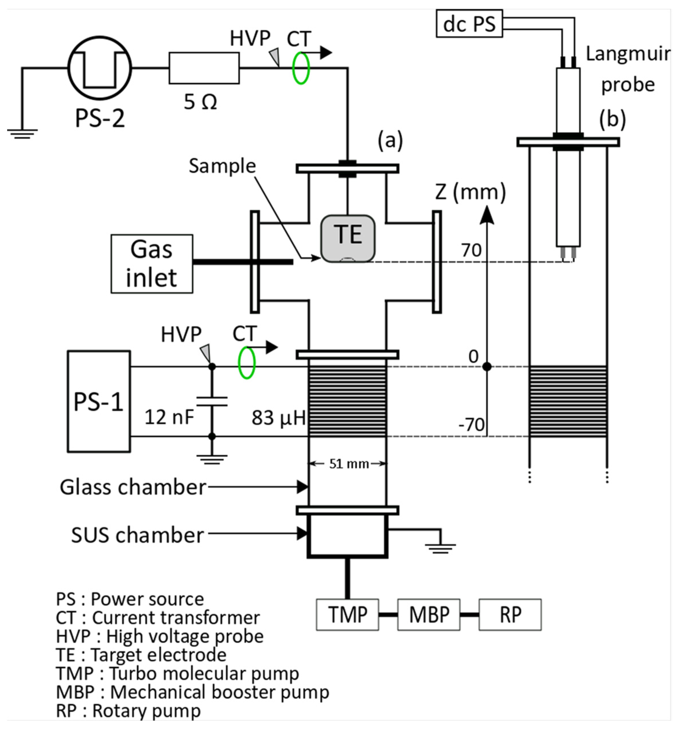
Abstract
:1. Introduction
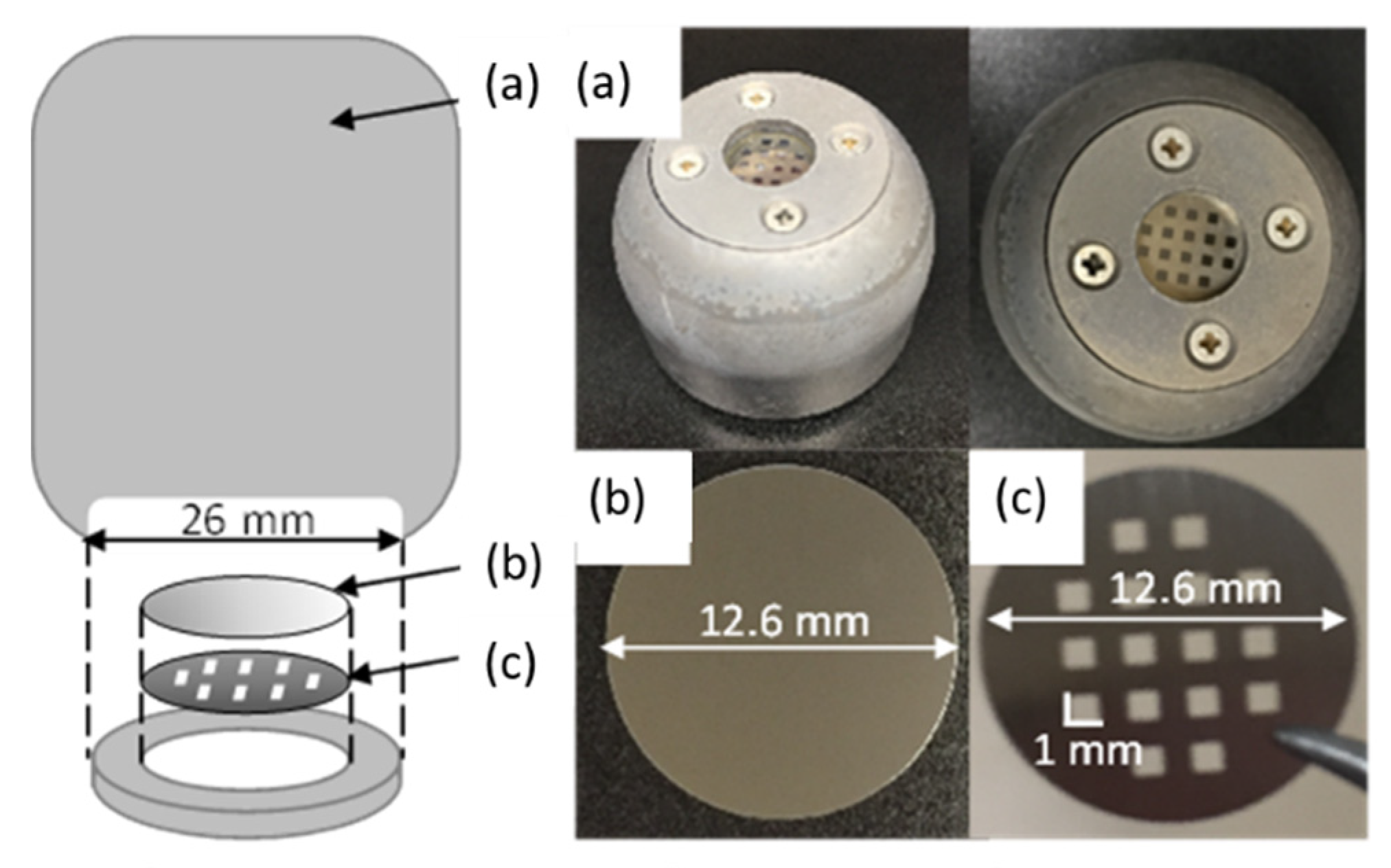
2. Experimental Procedure
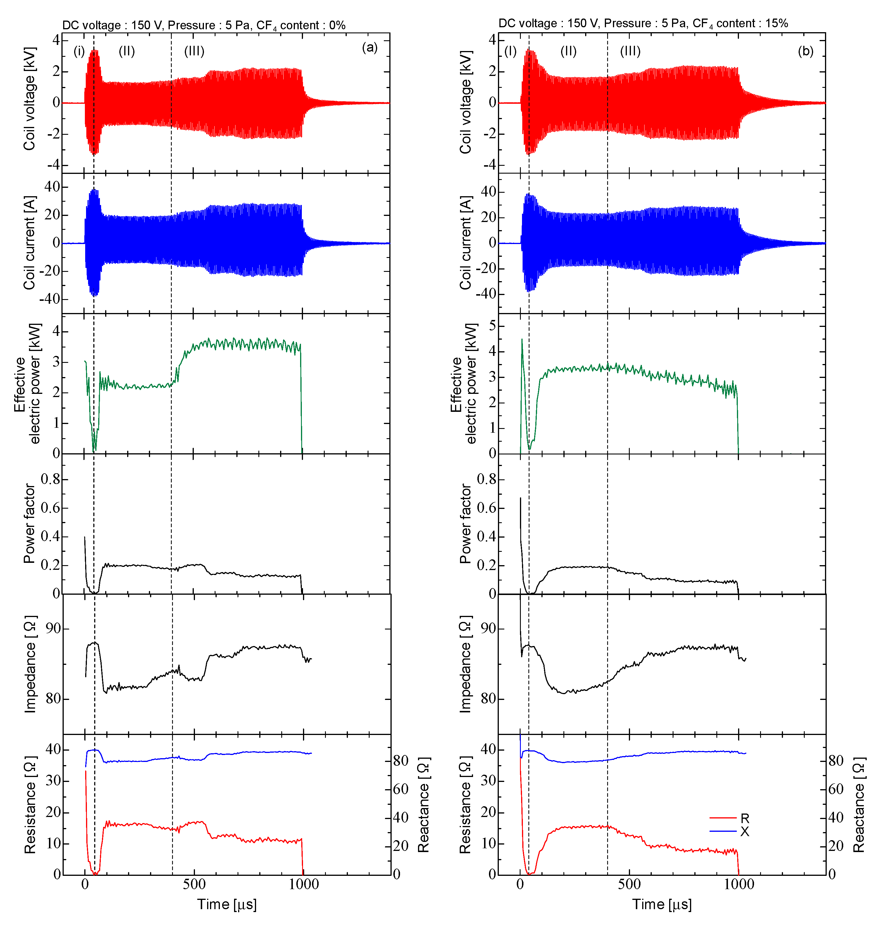
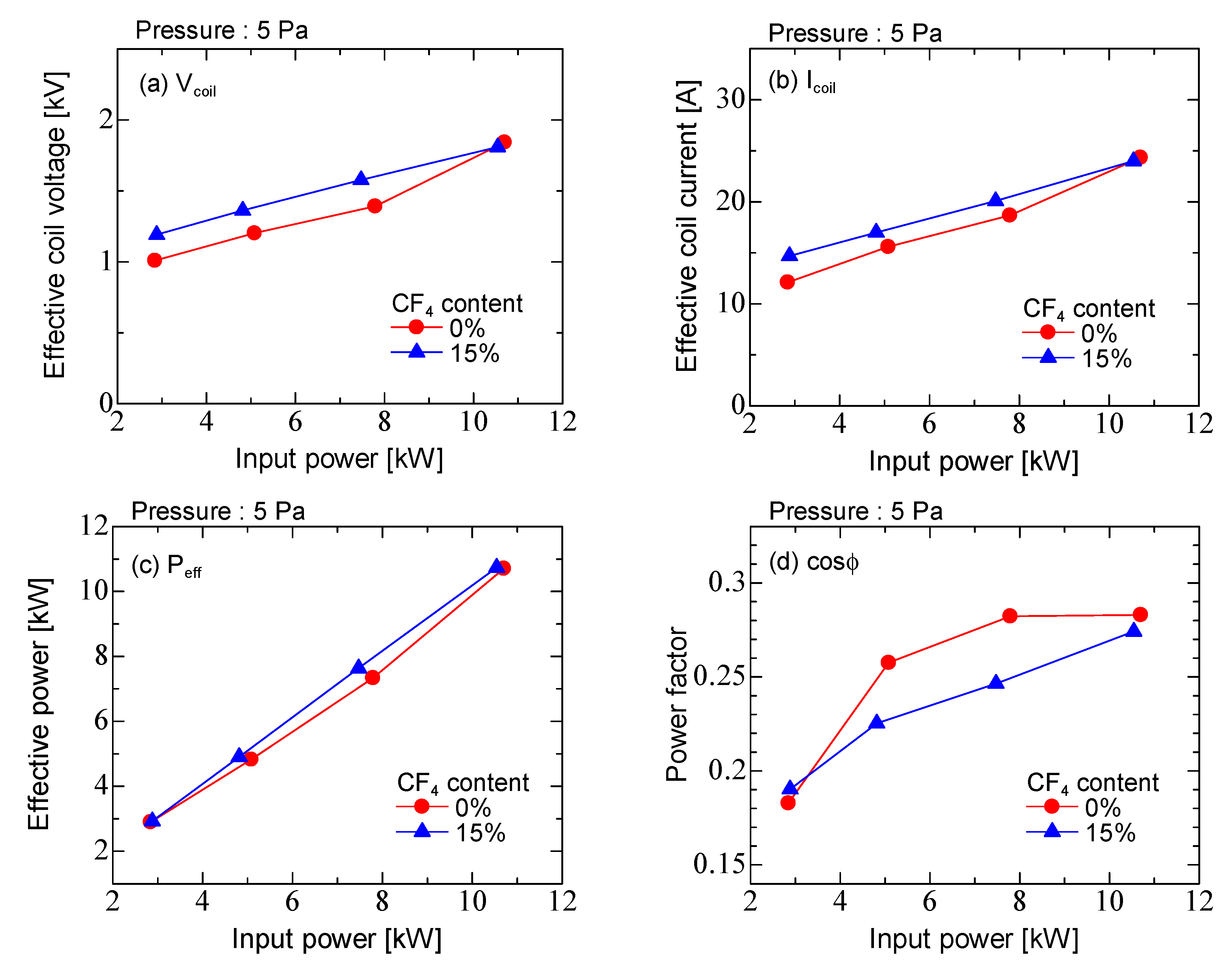
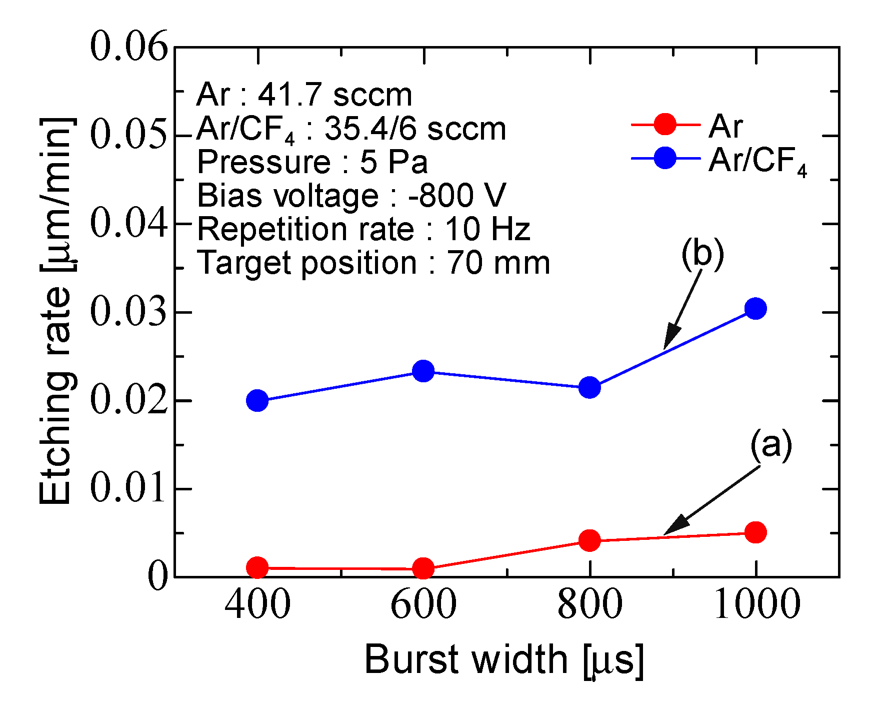
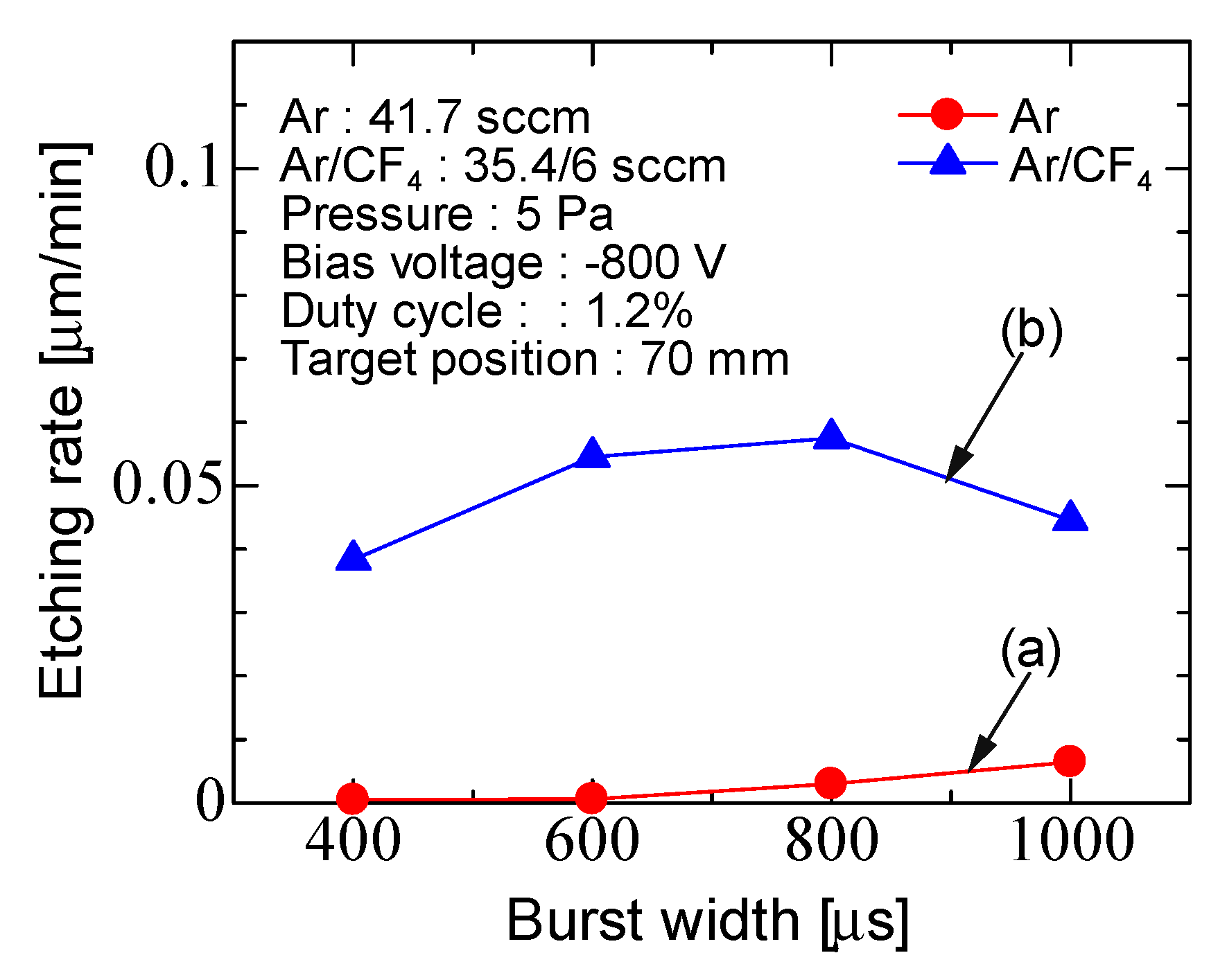
3. Results and Discussion
4. Conclusions
Author Contributions
Funding
Acknowledgments
Conflicts of Interest
References
- Helmersson, U.; Lattemann, M.; Bohlmark, J.; Ehiasarian, A.P.; Gudmundsson, J.T. Ionized physical vapor deposition (IPVD): A review of technology and applications. Thin Solid Films 2006, 513, 1–24. [Google Scholar] [CrossRef] [Green Version]
- Donnelly, V.M.; Kornblit, A. Plasma etching: Yesterday, today, and tomorrow. J. Vac. Sci. Technol. 2013, 31, 050825. [Google Scholar] [CrossRef] [Green Version]
- Hopwood, J. Ionized physical vapor deposition of integrated circuit interconnects. Phys. Plasma 1998, 5, 1624–1631. [Google Scholar] [CrossRef] [Green Version]
- Koyanagi, M.; Kurino, H.; Lee, K.W.; Sakuma, K.; Miyakawa, N.; Itani, H. Future System-on-Silicon LSI Chips. IEEE Micro. 1998, 18, 17–22. [Google Scholar] [CrossRef]
- Hopwood, J.; Search, H.; Journals, C.; Contact, A.; Iopscience, M.; Sci, P.S.; Address, I.P. Review of inductively coupled. Plasma Sources Sci. Technol. 1992, 1, 109–116. [Google Scholar] [CrossRef]
- Xu, S.; Ostrikov, K.N.; Li, Y.; Tsakadze, E.L.; Jones, I.R. Low-frequency, high-density, inductively coupled plasma sources: Operation and applications. Phys. Plasmas 2001, 8, 2549–2557. [Google Scholar] [CrossRef] [Green Version]
- Teske, C.J.; Jacoby, J. Pulsed low frequency inductively coupled plasma generator and applications. IEEE Trans. Plasma Sci. 2008, 36, 1930–1936. [Google Scholar] [CrossRef]
- Guo, W.; DeJoseph, C.A. Time-resolved current and voltage measurements on a pulsed rf inductively coupled plasma. Plasma Sources Sci. Technol. 2001, 10, 43–51. [Google Scholar] [CrossRef]
- Lieberman, M.A.; Lichtenberg, A.J. Principles of Plasma Discharges and Materials Processing, 2nd ed.; Wiley: New York, NY, USA, 2005. [Google Scholar]
- Makabe, T.; Petrovic, Z.L. Plasma electronics: Applications in Microelectronic Device Fabrication, 2nd ed.; CRC Press: New York, NY, USA, 2014. [Google Scholar]
- Tuszewski, M.; Scheuer, J.T.; Adler, R.A. A pulsed inductively coupled plasma source for plasma-based ion implantation. Surf. Coat. Technol. 1997, 93, 203–208. [Google Scholar] [CrossRef]
- Yukimura, K.; Ehiasarian, A.P. Generation of RF plasma assisted high power pulsed sputtering glow discharge without using a magnetic field. Nucl. Instrum. Methods Phys. Res. B 2009, 267, 1701–1704. [Google Scholar] [CrossRef]
- Yukirnnra, K.; Ogiso, H.; Nakano, S.; Ehiasarian, A.P. High-power inductively coupled impulse sputtering glow plasma. IEEE Trans. Plasma Sci. 2011, 39, 3085–3093. [Google Scholar]
- Yukimura, K.; Ogiso, H.; Nakano, S. Ionization of sputtered carbon species by high-power inductively-coupled impulse sputtering (ICIS). Vacuum 2018, 153, 195–203. [Google Scholar] [CrossRef]
- Shibata, K.; Konno, S.; Takahashi, K.; Mukaigawa, S.; Takaki, K.; Yukimura, K. Electrical and plasma characteristics of 150 kHz band high-power burst inductively coupled plasma. In Proceedings of the 2017 IEEE 21st International Conference on Pulsed Power, Brighton, UK, 18–22 June 2017. [Google Scholar]
- Saito, Y.; Shibata, K.; Takahashi, K.; Mukaigawa, S.; Takaki, K.; Yukimura, K. Global model analysis of Ar inductively coupled plasma driven by a 150 kHz-band high-power pulse burst. Jpn. J. Appl. Phys. 2019, 58, SAAB06. [Google Scholar] [CrossRef]
- Saito, Y.; Shibata, K.; Takahashi, K.; Mukaigawa, S.; Takaki, K.; Yukimura, K.; Ogiso, H.; Nakano, S. Silicon wafer etching by pulsed high-power inductively coupled Ar/CF4 plasma with 150 kHz band frequency. Jpn. J. Appl. Phys. 2020, 59, SHHE04. [Google Scholar] [CrossRef]
- Hara, S.; Maekawa, S.; Ikeda, S.; Nakano, S. Concept of minimal fab and development of minimal equipments. J. Jpn. Soc. Precis. Eng. 2011, 77, 249–253. [Google Scholar] [CrossRef]
- Yukimura, K.; Ogiso, H.; Nakano, S. Film deposition using 1-inch-sized HIPIMS system-Toward minimal fabrication semiconductor poduction system. Surf. Coat. Technol. 2014, 250, 26–31. [Google Scholar] [CrossRef]
- Johnson, E.O.; Malter, L. A floating double probe method for measurments in gas discharges. Phys. Rev. 1950, 80, 58–70. [Google Scholar] [CrossRef]
- Demidov, V.I.; Ratynskaia, S.V.; Rypdal, K. Electric probes for plasmas: The link between theory and instrument. Rev. Sci. Instrum. 2002, 73, 3409–3439. [Google Scholar] [CrossRef]
- Cherrington, B.E. The use of electrostatic probes for plasma diagnostics-A review. Plasma Chem. Plasma Process. 1982, 2, 113–140. [Google Scholar] [CrossRef]
- Yin, Y.; Messier, J.; Hopwood, J.A. Miniaturization of inductively coupled plasma sources. IEEE Trans. Plasma Sci. 1999, 27, 1516–1524. [Google Scholar] [CrossRef]
- Kimura, T.; Ohe, K. Electron energy distribution detection in symmetrically driven rf argon discharge. Jpn. J. Appl. Phys. 1993, 32, 3601–3605. [Google Scholar] [CrossRef]
- Piejak, R.B.; Godyak, V.A.; Alexandrovich, B.M. A simple analysis of an inductive RF discharge. Plasma Sources Sci. Technol. 1992, 1, 179–186. [Google Scholar] [CrossRef]
- Gudmundsson, J.T.; Lieberman, M.A. Magnetic induction and plasma impedance in a cylindrical inductive discharge. Plasma Sources Sci. Technol. 1997, 6, 540–550. [Google Scholar] [CrossRef]
- Chang, C.H.; Leou, K.C.; Chen, C.H.; Lin, C. Measurements of time resolved rf impedance of a pulsed inductively coupled Ar plasma. Plasma Sources Sci. Technol. 2006, 15, 338–344. [Google Scholar] [CrossRef]
- Cunge, G.; Crowley, B.; Vender, D.; Turner, M.M. Characterization of the E to H transition in a pulsed inductively coupled plasma discharge with internal coil geometry: Bi-stability and hysteresis. Plasma Sources Sci. Technol. 1999, 8, 576–586. [Google Scholar] [CrossRef]
- Yang, J.G.; Yoon, N.S.; Kirn, B.C.; Choi, J.H.; Lee, G.S.; Hwang, S.M. Power absorption characteristics of an inductively coupled plasma discharge. IEEE Trans. Plasma Sci. 1999, 27, 676–681. [Google Scholar] [CrossRef]
- Kortshagen, U.; Gibson, N.D.; Lawler, J.E. On the E-H mode transition in RF inductive discharges. J. Phys. D Appl. Phys. 1996, 29, 1224–1236. [Google Scholar] [CrossRef]
- Abe, S.; Takahashi, K.; Mukaigawa, S.; Takaki, K.; Yukimura, K. Comparison of plasma characteristics of high-power pulsed sputtering glow discharge and hollow-cathode discharge. Jpn. J. Appl. Phys. 2020, 60, 015501. [Google Scholar] [CrossRef]
- Hopwood, J.; Guarnieri, C.R.; Whitehair, S.J.; Cuomo, J.J. Electromagnetic fields in a radio-frequency induction plasma. J. Vac. Sci. Technol. 1993, 11, 147–151. [Google Scholar] [CrossRef]
- Haas, F.A.; Braithwaite, N.S.J. Tailoring of electron energy distributions in low-pressure inductive discharges. Appl. Phys. Letteers 1999, 74, 338–340. [Google Scholar] [CrossRef]
- Palmero, A.; Van Hattum, E.D.; Rudolph, H.; Habraken, F.H.P.M. Characterization of a low-pressure argon plasma using optical emission spectroscopy and a global model. J. Appl. Phys. 2007, 101, 053306. [Google Scholar] [CrossRef]
- Efremov, A.M.; Kim, D.P.; Kim, K.T.; Kim, C.I. Etching characteristics and mechanism of Pb(Zr,Ti)O3 thin films in CF4/Ar inductively coupled plasma. Vacuum 2004, 75, 321–329. [Google Scholar] [CrossRef]
- Kimura, T.; Ohe, K. Probe measurements and global model of inductively coupled Ar/CF4 discharge. Plasma Sources Sci. Technol. 1999, 8, 553–560. [Google Scholar] [CrossRef]
- Efremov, A.M.; Kim, D.P.; Kim, C.I. Effect of gas mixing ratio on gas-phase composition and etch rate in an inductively coupled CF4/Ar plasma. Vacuum 2004, 75, 133–142. [Google Scholar] [CrossRef]
- Zhao, S.X.; Gao, F.; Wang, Y.N.; Bogaerts, A. The effect of F 2 attachment by low-energy electrons on the electron behaviour in an Ar/CF 4 inductively coupled plasma. Plasma Sources Sci. Technol. 2012, 21, 025008. [Google Scholar] [CrossRef]
- Christophorou, L.G.; Olthoff, J.K.; Rao, M.V.V.S. Electron interactions with CF4. J. Phys. Chem. Ref. Data 1996, 25, 1341–1388. [Google Scholar] [CrossRef]
- Kumar, A.; Lee, W.H.; Wang, Y.L. Optimizing the isotropic etching nature and etch profile of Si, Ge and Si0.8Ge0.2 by controlling CF4 atmosphere with Ar and O2 additives in ICP. IEEE Trans. Semicond. Manuf. 2021, 34, 177–184. [Google Scholar] [CrossRef]


Publisher’s Note: MDPI stays neutral with regard to jurisdictional claims in published maps and institutional affiliations. |
© 2021 by the authors. Licensee MDPI, Basel, Switzerland. This article is an open access article distributed under the terms and conditions of the Creative Commons Attribution (CC BY) license (https://creativecommons.org/licenses/by/4.0/).
Share and Cite
Kikuchi, H.; Takahashi, K.; Mukaigawa, S.; Takaki, K.; Yukimura, K. Silicon Wafer Etching Rate Characteristics with Burst Width Using 150 kHz Band High-Power Burst Inductively Coupled Plasma. Micromachines 2021, 12, 599. https://doi.org/10.3390/mi12060599
Kikuchi H, Takahashi K, Mukaigawa S, Takaki K, Yukimura K. Silicon Wafer Etching Rate Characteristics with Burst Width Using 150 kHz Band High-Power Burst Inductively Coupled Plasma. Micromachines. 2021; 12(6):599. https://doi.org/10.3390/mi12060599
Chicago/Turabian StyleKikuchi, Hisaki, Katsuyuki Takahashi, Seiji Mukaigawa, Koichi Takaki, and Ken Yukimura. 2021. "Silicon Wafer Etching Rate Characteristics with Burst Width Using 150 kHz Band High-Power Burst Inductively Coupled Plasma" Micromachines 12, no. 6: 599. https://doi.org/10.3390/mi12060599