Article

High-Performance CVD Bilayer MoS2 Radio Frequency Transistors and Gigahertz Mixers for Flexible Nanoelectronics

1
School of Electronic Information, University of Electronic Science and Technology of China, Zhongshan Institute, Zhongshan 528402, China
2
School of Information and Communication Engineering, University of Electronic Science and Technology of China, Chengdu 611731, China
*
Author to whom correspondence should be addressed.
Micromachines 2021, 12(4), 451; https://doi.org/10.3390/mi12040451
Submission received: 27 March 2021 / Revised: 12 April 2021 / Accepted: 14 April 2021 / Published: 16 April 2021
(This article belongs to the Special Issue Electronic Devices and Circuits Based on 2D Materials)

Abstract

:
Two-dimensional (2D) MoS2 have attracted tremendous attention due to their potential applications in future flexible high-frequency electronics. Bilayer MoS2 exhibits the advantages of carrier mobility when compared with monolayer mobility, thus making the former more suitable for use in future flexible high-frequency electronics. However, there are fewer systematical studies of chemical vapor deposition (CVD) bilayer MoS2 radiofrequency (RF) transistors on flexible polyimide substrates. In this work, CVD bilayer MoS2 RF transistors on flexible substrates with different gate lengths and gigahertz flexible frequency mixers were constructed and systematically studied. The extrinsic cutoff frequency (fT) and maximum oscillation frequency (fmax) increased with reducing gate lengths. From transistors with a gate length of 0.3 μm, we demonstrated an extrinsic fT of 4 GHz and fmax of 10 GHz. Furthermore, statistical analysis of 14 flexible MoS2 RF transistors is presented in this work. The study of a flexible mixer demonstrates the dependence of conversion gain versus gate voltage, LO power and input signal frequency. These results present the potential of CVD bilayer MoS2 for future flexible high-frequency electronics.

1. Introduction

Owing to their ultimate thin thickness, superior mechanical flexibility and highly tunable electronic performance, two-dimensional materials for flexible applications have attracted tremendous attention [1,2,3,4,5]. Flexible transistors and devices based on 2D materials with high-speed are easy integrated with mature silicon CMOS manufacturing systems and can extend future flexible electronic systems even further with remote wireless capabilities. Recently, numerous devices and circuits using graphene, black phosphorous (BP) and molybdenum disulfide (MoS2) were demonstrated for radio-frequency flexible electronics [6,7,8,9,10,11,12,13]. Graphene, which has an extraordinary carrier mobility of over 10,000 cm2/Vs and a high saturation velocity, has caused many researchers to realize high-performance flexible RF electronics with this extraordinary material. However, the current saturation of graphene transistors is poor due to the lack of bandgap of graphene [1,14]. Therefore, as a result, most graphene RF transistors may have a relatively lower fmax, which limits power gain at high frequency. On the other hand, BP has a sizeable bandgap and moderate carrier mobility (1000 cm2/Vs), which makes it suitable for both low-power and high-speed flexible devices [13,15,16]. However, its poor reliability and lack of large-area high-quality growth capabilities are still the key technological barriers in BP high-frequency electronics [17].
Unlike graphene and BP, two-dimensional MoS2 with long-term air stability has a sizable bandgap, relative moderate carrier mobility and saturation velocity, and large-area growth capability. As an atomically thin semiconductor, 2D MoS2 have demonstrated great potential for use in high-frequency electronics, next-generation logic circuits and flexible electronics [9,18,19,20,21,22]. In 2014, radio-frequency transistors fabricated using exfoliated MoS2 demonstrated an extrinsic fT of 2.1 GHz and fmax of 8 GHz on rigid Si/SiO2 substrates [22]. In the same year, exfoliated few-layer MoS2 RF transistors with self-aligned gates on rigid quartz and flexible polyimide substrates were reported [9]. The frequency responses of the self-aligned transistors on rigid quartz substrate showed an extrinsic fT of 10.2 GHz and fmax of 14.5 GHz; a gigahertz inverter and amplifier were also demonstrated. Additionally, the frequency response of the self-aligned transistors on flexible PI substrate shown an extrinsic fT and fmax of 4.7 and 5.4 GHz, respectively. Recently, Zhang et al. presented an flexible rectenna based on MoS2 high-frequency diodes with a cutoff frequency of 10 GHz [18]. Although these works have demonstrated the potential of high-frequency MoS2 devices, exfoliated MoS2 lack precise control of flake size and thickness, which hamper large-scale commercial manufacturing and applications [23,24].
Chemical vapor deposition (CVD) is a low-cost and important method to produce large-area, high-quality MoS2 film. High-quality uniform CVD monolayer MoS2 film larger than two inches has been growth by different groups [4,23,24,25]. In 2015, RF transistors based on CVD monolayer MoS2 with an extrinsic fT of 2.8 GHz and fmax of 3.6 GHz were reported, and simple circuit demos, such as the megahertz MoS2 frequency mixer and common-source amplifier, were also demonstrated [26]. As has been done with exfoliated MoS2, optimized gate configuration was applied to CVD MoS2 transistors to achieve higher cut-off frequencies [27]. With optimized embedded gate structure, CVD monolayer MoS2 transistors with improved extrinsic fT of 3.3 GHz and fmax of 9.8 GHz were fabricated. Although the RF performance of CVD MoS2 transistors was advanced with optimized device configuration, neither fT nor fmax can reach the level of exfoliated MoS2 transistors, which severely limits their high-frequency applications. Bilayer MoS2 usually has higher carrier mobility and higher density of states, which in turn will result in superior performance over electronic devices based on monolayers [28,29,30]. In 2018, CVD bilayer MoS2 RF transistors with extrinsic fT of 7.2 GHz and fmax of 23 GHz were demonstrated. For flexible high frequency transistors, extrinsic fT and fmax of 2.7 and 2.1 GHz were obtained based on CVD monolayer MoS2 [11], and the extrinsic fT and fmax of 4 and 9 GHz were obtained based on CVD bilayer MoS2 [31]. Although flexible MoS2 RF transistors based on CVD bilayer MoS2 have been demonstrated, there still many problems that need to be investigated. The reported flexible CVD bilayer MoS2 RF transistors only have one gate length. Its scaling behavior is still unexplored. Additionally, statistical analysis of MoS2 flexible RF transistors with different gate lengths needs more research, which is important to understand the uniformity of MoS2 RF transistors and helpful to acquire deep insight into the limited factor of large-scale high performance MoS2 RF transistors [32].
In this work, a systematic study of CVD bilayer MoS2 RF transistors on flexible substrates is presented. First, high-quality chemical vapor deposited bilayer MoS2 were grown on molten glass and transferred onto a Si3N4/PI substrate. The fabrication process of flexible high-frequency MoS2 transistors was presented. An extrinsic field-effect mobility of 5 cm2/Vs and a high Ion/Ioff ratio of 108 were demonstrated with flexible bilayer MoS2 transistors. High-frequency measurements up to 10 GHz and statistical analysis were carried out for 14 MoS2 RF transistors with gate lengths of 0.3 μm, 0.6 μm, and 1 μm. Cut-off frequency and maximum oscillation frequency increased as the gate length was scaled down. Extrinsic fT of 4 GHz and fmax of 10 GHz were achieved for the 0.3 μm transistors. Additionally, the transistors with larger gate length had better high-frequency performance uniformity. Finally, conversion gain of gigahertz MoS2 frequency mixer versus gate voltage, frequency and input power were systematically investigated.

2. Materials and Methods

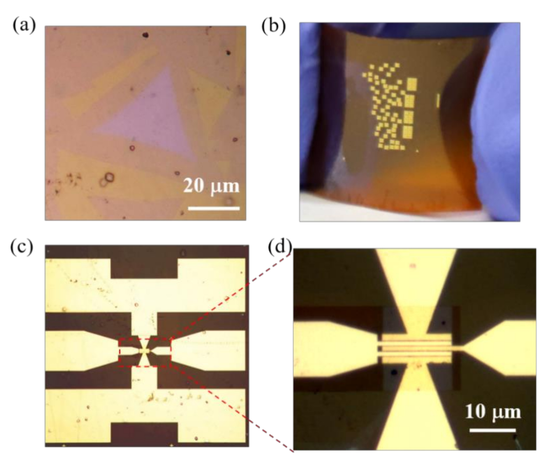
2.1. Material Growth and Characterization

The bilayer MoS2 films were grown on molten glass substrates using sulfur powders and MoO3 powders as reaction precursors in a two-zone furnace. Then, an alumina crucible with 1.4 g sulfur powder and a quartz crucible with 2 mg MoO3 precursor and glass substrates were placed at the center of first and second heating zones, respectively. The distance between the MoO3 precursor and glass substrates was about 2 mm. The temperatures of the first and second zones were ramped to 230 °C and 830 °C, respectively. During the ramping and growth process, a 40 sccm Ar flow was introduced as the carrier gas, and the pressure within the quartz tube was controlled to 1 atm pressure. After a growth duration of 10 min, the furnace was turned off, and the system began to cool down. Figure 1a shows a typical optical microscopy of the bilayer; MoS2 with a triangular shape shows a highly uniform color contrast in the bilayer region, indicating homogenous thickness. The thickness and quality of the CVD bilayer MoS2 were then characterized by an atomic force microscope (AFM), Raman spectroscopy and photoluminescence analyses. Figure 1b shows the AFM image of the edge of the bilayer MoS2, and the corresponding height profile presents a thickness of 1.34 nm [33]. As shown in Figure 1c, after being transferred onto SiO2/Si substrates, the bilayer MoS2 shows typical Raman spectra with an E12g peak of 385.7 cm−1 and A1g peak of 408.3 cm−1. The delta value between the E12g and A1g peaks is 22.6 cm−1, which is consistent with previous reports of bilayer MoS2 [34,35,36]. The typical photoluminescence (PL) spectrum of the bilayer MoS2 is shown in Figure 1d, where the peaks at around 665 and 618 nm correspond to the A1 and B1 direct excitonic transitions at 1.86 and 2.01 eV, respectively [31,37]. What’s more, as shown in Figure S1, further elemental analysis of the CVD-grown MoS2 was studied by X-ray photoelectron spectroscopy (XPS). More details about material characterizations of CVD-grown MoS2 can be found in our previous works [31].

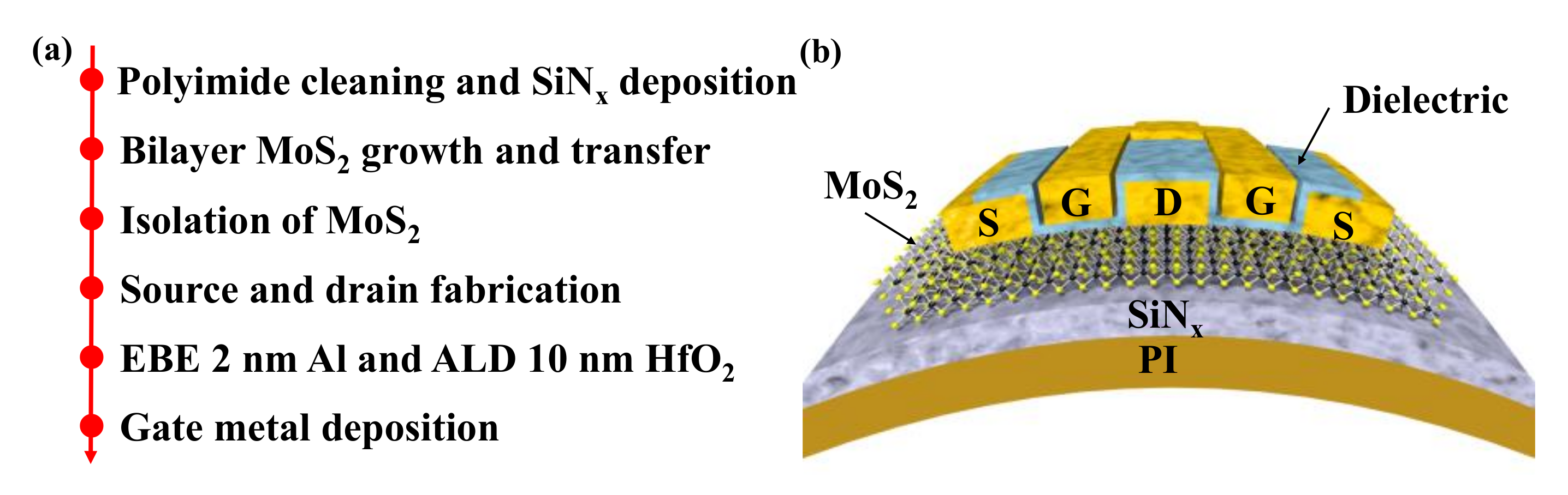
2.2. Device Fabrication

Figure 2 shows the fabrication process flows and device schematic of the bilayer MoS2 RF devices on flexible polyimide substrates. Prior to fabrication, the commercially available PI substrates (Dupont Kapton 500HN) were cleaned in acetone, isopropyl alcohol (IPA) and deionized water. To reduce the surface roughness, 100 nm of Si3N4 were deposited by plasma-enhanced CVD (PECVD). Then, bilayer MoS2 films were transferred onto polyimide substrates via the polymethyl methacrylate (PMMA)-assisted transfer method [23,25]. Different from conventional acidic or alkaline solutions as etchant, deionized water was utilized here for the hydrophobicity/hydrophilicity property of the as-grown MoS2/glass stack. As shown in Figure 3a, the high-quality triangle shape of bilayer MoS2 was well preserved, which is important for the fabrication of high-performance MoS2 transistors. After the transfer process, bilayer MoS2 films were patterned with an electron beam lithography (EBL) step and etched using O2/Ar plasma. Source and drain contact electrodes were formed by electron beam evaporation (EBE) with 20/60-nm Ni/Au metal stacks. To form a uniform top-gate dielectric, 2-nm Al was grown by EBE as a seed layer before the atomic layer deposition of HfO2. Finally, the two-fingers top-gate electrode of 20/60-nm Ni/Au was defined by EBL and deposited by EBE. The high-frequency bilayer MoS2 transistors on flexible PI substrates after fabrication are shown in Figure 3b,c. In this work, the MoS2 RF transistors are designed with different gate lengths of 0.3 μm, 0.6 μm, and 1 μm and the same gate width of 2 × 15 μm. Figure 3d shows an optical microscope of a device with a gate length of 1 μm, exhibiting the precise alignment of the gate structure to the source/drain area. From the theory of high-frequency electronics, both gate to drain/source capacitance Cgd/Cgs and series resistance are critical factors in high-performance RF transistors. In this device design, there is no overlap between gate and source/drain electrodes to avoid excess Cgd and Cgs. Additionally, the gate to source/drain access lengths Lgs and Lgd are minimized to decrease the series resistance.

3. Results and Discussion

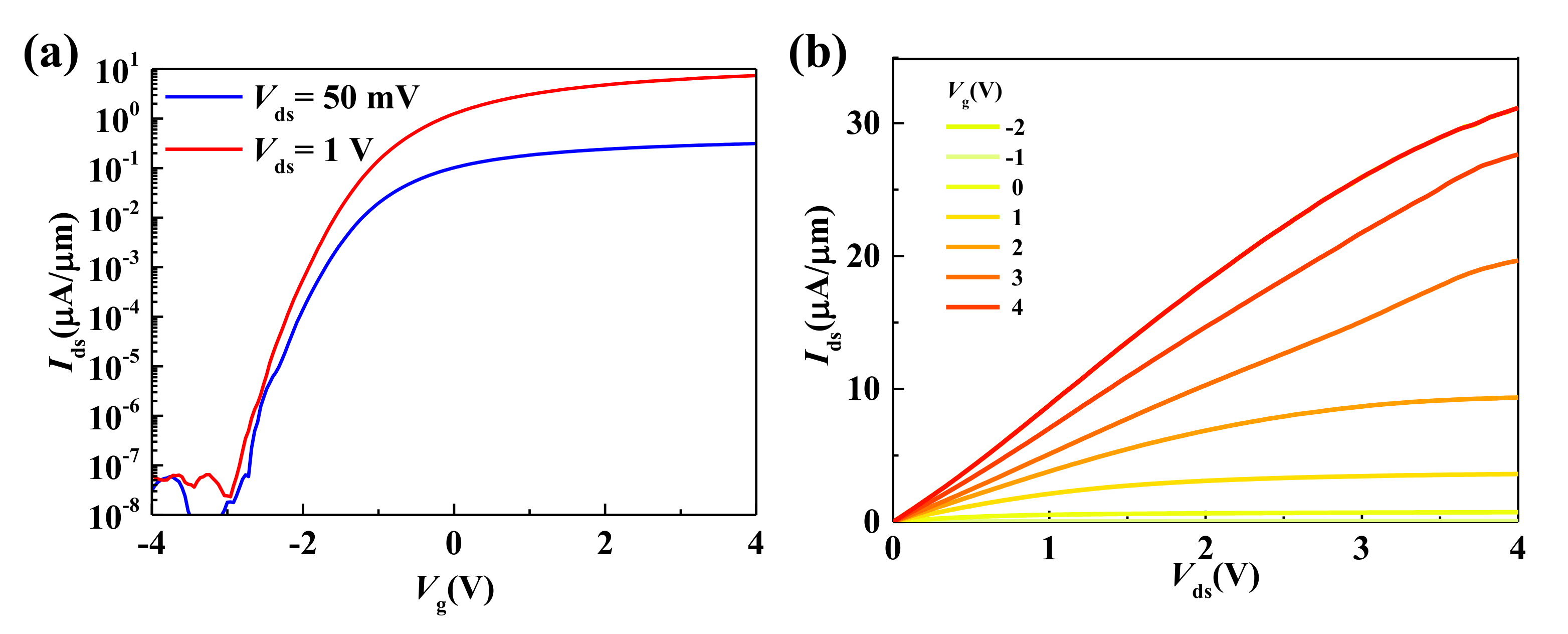
3.1. DC Characterization

Figure 4a,b shows the measured transfer and output characteristics of CVD bilayer MoS2 transistors on polyimide substrates. A high Ion/Ioff ratio of 108 is achieved, making these devices ideal for ultra-low power applications. The extrinsic low-field effect mobility of 5 cm2/Vs is extracted. Here, we note that the extracted mobility value is underestimated as there is a non-negligible contact resistance contribution to the total device resistance. The intrinsic mobility of our bilayer MoS2 on rigid substrates is calculated to be 36 cm2/Vs [31]. The degradation of mobility can be attributed to the increased surface roughness and poor thermal conductivity of organic flexible substrates. The output characteristics of bilayer MoS2 transistors on polyimide shows applicable current saturation. An on-current density of 30 μA/μm was demonstrated with the Lg = 1 μm device. For comparison, we also fabricated flexible monolayer MoS2 transistors on polyimide substrates. An extrinsic carrier mobility of 0.2 cm2/Vs and an on-current density of 1.2 μA/μm were obtained with the same gate length, showing the superiority of CVD bilayer MoS2 for flexible electronic applications.

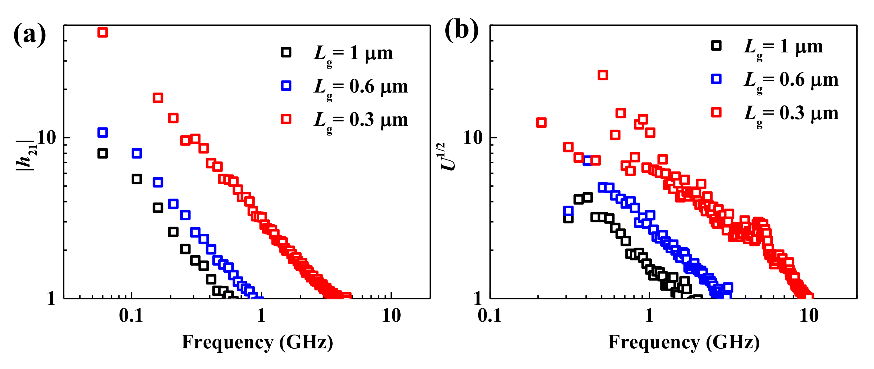
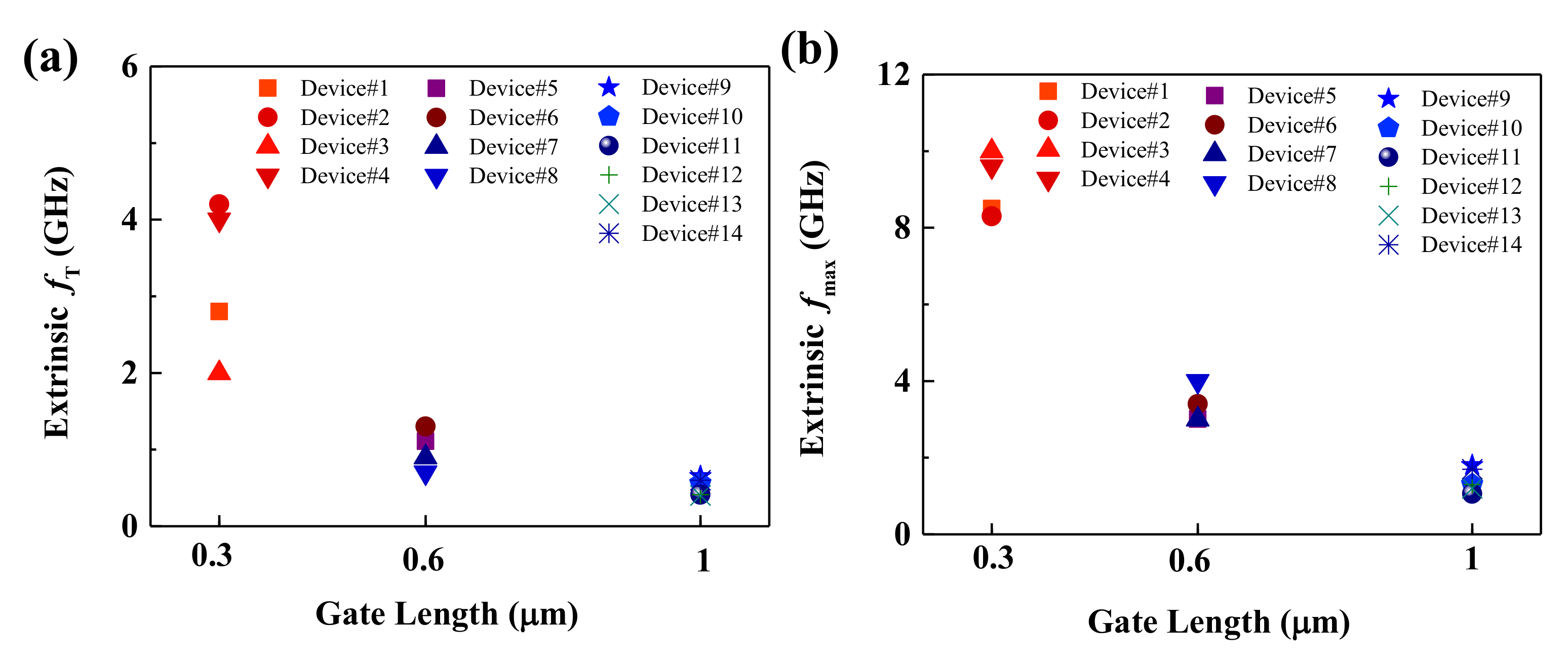
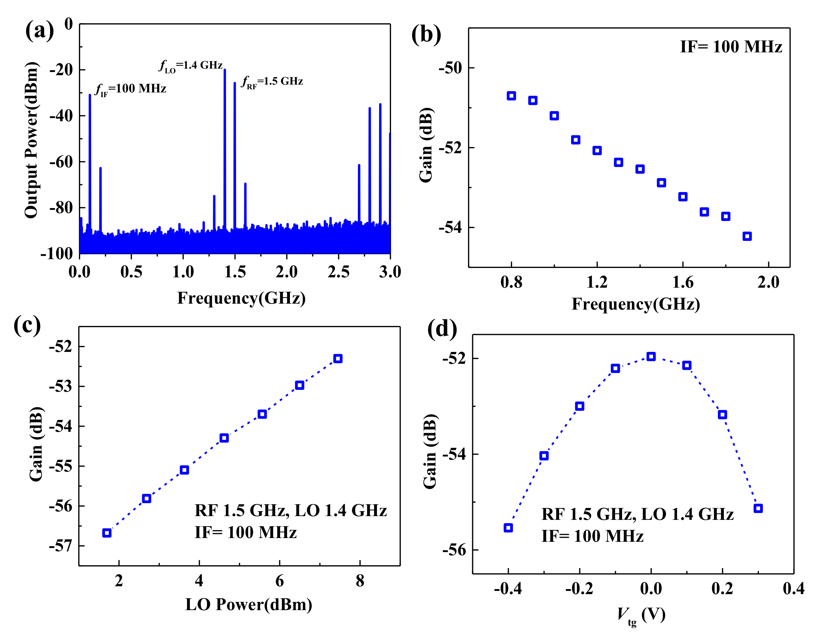
3.2. RF Characterization

Cutoff frequency fT and maximum oscillation frequency fmax are commonly used to characterize the high-frequency performance of RF transistors. fT corresponds to the frequency where the short-circuit current gain becomes unity. From the small signal equivalent circuit of the transistor, fT can be described using
f T = g m 2 π 1 ( C gs + C gd ) [ 1 + g ds ( R s + R d ) ] + C gd g m ( R s + R d )
where Cgs is the gate to source capacitance, Cgd is the gate to drain capacitance, gm is the transconductance, gds is the output conductance, and Rs and Rd are the source and drain series resistances, respectively. fmax correspond to the frequency where the unilateral power gain becomes unity. fmax can be described using
f max = f T 2 g ds ( R s + R d ) + 2 π f T C g R g
where Rg is the gate resistance, which can be reduced through the increase of gate metal area and thickness. To evaluate the high-frequency performance of the CVD bilayer MoS2 transistors, standard on-chip S-parameter measurements up to 10 GHz were performed. Figure 5a,b show the as-measured extrinsic small-signal current gain (|h21|) and Mason’s unilateral power gain (U) as a function of frequency for the CVD bilayer MoS2 transistors. An extrinsic fT of 4 GHz and fmax of 10 GHz were achieved where, as shown in Table 1, the fmax is the highest extrinsic maximum oscillation frequency among flexible MoS2 RF transistors [9,11], demonstrating the potential of bilayer MoS2 for large-scale, high-performance RF applications. What’s more, fmax is also comparable to MoS2 transistors on rigid substrates with the same gate length [31]. This can be attributed to the decreased high-frequency parasitic effect in insulating polyimide substrates, although the roughness and poor thermal conductivity of polyimide substrates degrade the DC transport performance of the MoS2 transistors [12].
Figure 6, displaying the devices’ data, gives some insight into the statistical analysis and scalability of CVD bilayer MoS2 RF transistors on flexible PI substrates. The extrinsic fT and fmax of 14 MoS2 devices with different gate lengths are plotted in Figure 6a,b, respectively. Both fT and fmax increase as the gate length decreases. Additionally, through gate length scaling down, it is possible to further improve the fT and fmax. Variations of fT and fmax within devices of the same gate length can be observed, especially for transistors with a gate length of 0.3 μm. Here, we attribute these variations to the varied alignment of gate and source/drain electrodes in the EBL process of short gate length transistors. Since flexible organic substrates are not conductive and easily result in deformation, not all devices in this work could realize the perfect alignment of gate and source/drain electrodes, as shown in Figure 3d. Short gate length RF transistors are more prone to uniformity problems. Therefore, the contact resistance, substrate roughness and fabrication process are still critical limitations of flexible bilayer MoS2 RF transistors. It should be pointed out that MoS2 transistors with 1T phase electrodes exhibiting contact resistance of 200–300 Ω∙μm have been demonstrated [38]. MoS2 polymorphs with diverse electrical properties and their applications in high-frequency nanoelectronics are fascinating [18,38,39,40,41,42,43] and require further investigation.
Although flexible MoS2 mixers have been demonstrated in previous work [11,31], the frequency response and gate bias voltage dependence of flexible MoS2 mixers have not been reported. In this work, active mixers based on flexible bilayer MoS2 transistors were demonstrated and systematically researched. Mixer measurements were carried out at room temperature with an RF input frequency of 1.5 GHz and local oscillation (LO) frequency of 1.4 GHz. Figure 7a shows the measured IF output signal (0.1 MHz) using a signal analyzer. The conversion gain versus the input frequency is plotted in Figure 7b. When the input signal powers and fIF of 100 MHz are the same, conversion gain decreases as frequency increase from 0.8 to 1.9 GHz. Figure 7c shows the conversion gain versus LO power. A conversion gain of −52.3 dB could be achieved with fRF of 1.5 GHz. For the flexible active MoS2 mixer, as shown in Figure 7d, gate bias voltage is important to achieve the maximum conversion gain. This is because DC transconductance, the same as cutoff frequency and maximum oscillation frequency, has a strong dependence on gate bias voltage.

4. Conclusions

In this work, we constructed high-frequency transistors and gigahertz mixers on flexible polyimide substrates based on CVD bilayer MoS2, and their high-frequency performance was systematically assessed. Record extrinsic fmax as high as 10 GHz have been demonstrated with 0.3 μm devices. The scaling behavior of MoS2 RF transistors on flexible polyimide substrates was studied, and the extrinsic fT and fmax were increased as gate length decreased, showing the potential for further improvement through decreasing the gate lengths. Statistical analysis of 14 flexible MoS2 RF transistors with different gate length showed RF performance variation in short gate length MoS2 transistors. We systematically studied the dependence of flexible MoS2 mixer conversion gain on gate bias voltage, fRF and LO power, addressing the importance of Vtg, LO power and fRF on high-performance flexible MoS2 mixers. Our results advance the achieved maximum oscillation frequency of flexible CVD MoS2 transistors and represent a step towards high-performance flexible MoS2 wireless communications systems.

Supplementary Materials

The following are available online at https://www.mdpi.com/article/10.3390/mi12040451/s1, Figure S1: (a) The XPS spectra of the Mo 3d state, (b) S 2s state.

Author Contributions

Conceptualization, Q.G. and C.Z.; methodology, Q.G., K.Y. and X.P.; validation, Q.G. and Z.Z.; formal analysis, Q.G., Z.Z. and X.P.; investigation, Q.G.; resources, C.Z., Z.Y., J.Y., F.C. and L.L.; data curation, Q.G.; writing—original draft preparation, Q.G. and C.Z.; writing—review and editing, Q.G. and C.Z.; visualization, Q.G.; supervision, Q.G. and C.Z.; project administration, Q.G. and C.Z.; funding acquisition, Q.G., Z.Y. and C.Z. All authors have read and agreed to the published version of the manuscript.

Funding

This work was funded in part by the Guangdong Basic and Applied Basic Research Foundation (Grant No. 2019A1515110752), in part by the Youth Innovative Talent Project of Guangdong Education Department (Grant No. 2019KQNCX187), in part by the Outstanding Chinese and Foreign Youth Exchange Program of China Association for Science and Technology (CAST), 2019, in part by the Natural Science Foundation of China (Grant No. 62071088), and in part by the Project for Innovation Team of Guangdong University (Grant No. 2018KCXTD033), in part by National Key R&D Program of China (Grant No. 2018YFB1801302), in part by Zhongshan Social Public Welfare Science and Technology (Grant No. 2019B2007), in part by Research Project for Talent of UESTC Zhongshan Institute (419YKQN09).

Data Availability Statement

The data that support the findings of this study are available from the corresponding author upon reasonable request.

Conflicts of Interest

The authors declare no conflict of interest.

References

  1. Akinwande, D.; Huyghebaert, C.; Wang, C.-H.; Serna, M.I.; Goossens, S.; Li, L.-J.; Wong, H.-S.P.; Koppens, F.H.L. Graphene and two-dimensional materials for silicon technology. Nat. Cell Biol. 2019, 573, 507–518. [Google Scholar] [CrossRef]
  2. Li, C.; Xiong, K.; Li, L.; Guo, Q.; Chen, X.; Madjar, A.; Watanabe, K.; Taniguchi, T.; Hwang, J.C.M.; Xia, F. Black Phosphorus High-Frequency Transistors with Local Contact Bias. ACS Nano 2020, 14, 2118–2125. [Google Scholar] [CrossRef]
  3. Xiong, X.; Huang, M.; Hu, B.; Li, X.; Liu, F.; Li, S.; Tian, M.; Li, T.; Song, J.; Wu, Y. A transverse tunnelling field-effect tran-sistor made from a van der Waals heterostructure. Nat. Electron. 2020, 3, 106–112. [Google Scholar] [CrossRef]
  4. Yang, P.; Zhang, S.; Pan, S.; Tang, B.; Liang, Y.; Zhao, X.; Zhang, Z.; Shi, J.; Huan, Y.; Shi, Y.; et al. Epitaxial Growth of Centimeter-Scale Single-Crystal MoS2 Monolayer on Au(111). ACS Nano 2020, 14, 5036–5045. [Google Scholar] [CrossRef] [PubMed]
  5. Gao, Q.; Li, X.; Tian, M.; Xiong, X.; Zhang, Z.; Wu, Y. Short-Channel Graphene Mixer with High Linearity. IEEE Electron. Device Lett. 2017, 38, 1168–1171. [Google Scholar] [CrossRef]
  6. Pu, J.; Yomogida, Y.; Liu, K.-K.; Li, L.-J.; Iwasa, Y.; Takenobu, T. Highly flexible MoS2 thin-film transistors with ion gel die-lectrics. Nano Lett. 2012, 12, 4013–4017. [Google Scholar] [CrossRef] [PubMed]
  7. Chang, H.-Y.; Yang, S.; Lee, J.; Tao, L.; Hwang, W.-S.; Jena, D.; Lu, N.; Akinwande, D. High-Performance, Highly Bendable MoS2 Transistors with High-K Dielectrics for Flexible Low-Power Systems. ACS Nano 2013, 7, 5446–5452. [Google Scholar] [CrossRef] [PubMed] [Green Version]
  8. Akinwande, D.; Petrone, N.; Hone, J. Two-dimensional flexible nanoelectronics. Nat. Commun. 2014, 5, 5678. [Google Scholar] [CrossRef] [PubMed]
  9. Cheng, R.; Jiang, S.; Chen, Y.; Liu, Y.; Weiss, N.; Cheng, H.-C.; Wu, H.; Huang, Y.; Duan, X. Few-layer molybdenum disul-fide transistors and circuits for high-speed flexible electronics. Nat. Commun. 2014, 5, 5143. [Google Scholar] [CrossRef]
  10. Park, J.; Choudhary, N.; Smith, J.; Lee, G.; Kim, M.; Choi, W. Thickness modulated MoS2 grown by chemical vapor deposi-tion for transparent and flexible electronic devices. Appl. Phys. Lett. 2015, 106, 012104. [Google Scholar] [CrossRef] [Green Version]
  11. Chang, H.-Y.; Yogeesh, M.N.; Ghosh, R.; Rai, A.; Sanne, A.; Yang, S.; Lu, N.; Banerjee, S.K.; Akinwande, D. Large-Area Monolayer MoS2 for Flexible Low-Power RF Nanoelectronics in the GHz Regime. Adv. Mater. 2016, 28, 1818–1823. [Google Scholar] [CrossRef]
  12. Park, S.; Shin, S.H.; Yogeesh, M.N.; Lee, A.L.; Rahimi, S.; Akinwande, D. Extremely High-Frequency Flexible Graphene Thin-Film Transistors. IEEE Electron. Device Lett. 2016, 37, 512–515. [Google Scholar] [CrossRef]
  13. Zhu, W.; Park, S.; Yogeesh, M.N.; McNicholas, K.M.; Bank, S.R.; Akinwande, D. Black phosphorus flexible thin film transis-tors at gighertz frequencies. Nano Lett. 2016, 16, 2301–2306. [Google Scholar] [CrossRef] [PubMed]
  14. Wu, Y.; Lin, Y.-M.; Bol, A.A.; Jenkins, K.A.; Xia, F.; Farmer, D.B.; Zhu, Y.; Avouris, P. High-frequency, scaled graphene tran-sistors on diamond-like carbon. Nature 2011, 472, 74–78. [Google Scholar] [CrossRef]
  15. Liu, H.; Neal, A.T.; Zhu, Z.; Luo, Z.; Xu, X.; Tománek, D.; Ye, P.D. Phosphorene: An Unexplored 2D Semiconductor with a High Hole Mobility. ACS Nano 2014, 8, 4033–4041. [Google Scholar] [CrossRef] [PubMed] [Green Version]
  16. Wang, H.; Wang, X.; Xia, F.; Wang, L.; Jiang, H.; Xia, Q.; Chin, M.L.; Dubey, M.; Han, S.-J. Black phosphorus radio-frequency transistors. Nano Lett. 2014, 14, 6424–6429. [Google Scholar] [CrossRef] [PubMed] [Green Version]
  17. Wan, D.; Huang, H.; Wang, Z.; Liu, X.; Liao, L. Recent advances in long-term stable black phosphorus transistors. Nanoscale 2020, 12, 20089–20099. [Google Scholar] [CrossRef] [PubMed]
  18. Zhang, X.; Grajal, J.; Vazquez-Roy, J.L.; Radhakrishna, U.; Wang, X.; Chern, W.; Zhou, L.; Lin, Y.; Shen, P.-C.; Ji, X.; et al. Two-dimensional MoS2-enabled flexible rectenna for Wi-Fi-band wireless energy harvesting. Nat. Cell Biol. 2019, 566, 368–372. [Google Scholar] [CrossRef]
  19. Lin, Z.; Liu, Y.; Halim, U.; Ding, M.; Liu, Y.; Wang, Y.; Jia, C.; Chen, P.; Duan, X.; Wang, C.; et al. Solution-processable 2D semiconductors for high-performance large-area electronics. Nat. Cell Biol. 2018, 562, 254–258. [Google Scholar] [CrossRef]
  20. Desai, S.B.; Madhvapathy, S.R.; Sachid, A.B.; Llinas, J.P.; Wang, Q.; Ahn, G.H.; Pitner, G.; Kim, M.J.; Bokor, J.; Hu, C.; et al. MoS2 transistors with 1-nanometer gate lengths. Science 2016, 354, 99–102. [Google Scholar] [CrossRef] [Green Version]
  21. Tasker, P.J.; Hughes, B. Importance of source and drain resistance to the maximum fT of millimeter-wave MODFETs. IEEE Electron. Device Lett. 1989, 10, 291–293. [Google Scholar] [CrossRef]
  22. Krasnozhon, D.; Lembke, D.; Nyffeler, C.; Leblebici, Y.; Kis, A. MoS2 Transistors Operating at Gigahertz Frequencies. Nano Lett. 2014, 14, 5905–5911. [Google Scholar] [CrossRef] [PubMed] [Green Version]
  23. Wang, Q.; Li, N.; Tang, J.; Zhu, J.; Zhang, Q.; Jia, Q.; Lu, Y.; Wei, Z.; Yu, H.; Zhao, Y.; et al. Wafer-Scale Highly Oriented Monolayer MoS2 with Large Domain Sizes. Nano Lett. 2020, 20, 7193–7199. [Google Scholar] [CrossRef] [PubMed]
  24. Guangyu, Z.; Liao, M.; Zhao, W.; Liu, G.; Zhou, X.J.; Wei, Z.; Xu, X.; Liu, K.; Hu, Z.; Deng, K.; et al. Wafer-Scale Growth and Transfer of Highly-Oriented Monolayer MoS2 Continuous Films. ACS Nano 2017, 11, 12001–12007. [Google Scholar] [CrossRef]
  25. Yang, P.; Zou, X.; Zhang, Z.; Zhongfan, L.; Shi, J.; Chen, S.; Shulin, C.; Zhao, L.; Jiang, S.; Zhou, X.; et al. Batch production of 6-inch uniform monolayer molybdenum disulfide catalyzed by sodium in glass. Nat. Commun. 2018, 9, 1–10. [Google Scholar] [CrossRef]
  26. Sanne, A.; Ghosh, R.; Rai, A.; Yogeesh, M.N.; Shin, S.H.; Sharma, A.; Jarvis, K.; Mathew, L.; Rao, R.; Akinwande, D.; et al. Radio Frequency Transistors and Circuits Based on CVD MoS. Nano Lett. 2015, 15, 5039–5045. [Google Scholar] [CrossRef] [PubMed]
  27. Sanne, A.; Park, S.; Ghosh, R.; Yogeesh, M.N.; Liu, C.; Mathew, L.; Rao, R.; Akinwande, D.; Banerjee, S.K. Embedded gate CVD MoS2 microwave FETs. NPJ 2D Mater. Appl. 2017, 1, 26. [Google Scholar] [CrossRef] [Green Version]
  28. Wang, X.; Feng, H.; Wu, Y.; Jiao, L. Controlled Synthesis of Highly Crystalline MoS2 Flakes by Chemical Vapor Deposition. J. Am. Chem. Soc. 2013, 135, 5304–5307. [Google Scholar] [CrossRef]
  29. Zobel, A.; Boson, A.; Wilson, P.M.; Muratov, D.S.; Kuznetsov, D.V.; Sinitskii, A. Chemical vapour deposition and character-ization of uniform bilayer and trilayer MoS2 crystals. J. Mater. Chem. C 2016, 4, 11081–11087. [Google Scholar] [CrossRef]
  30. Jeon, J.; Jang, S.K.; Jeon, S.M.; Yoo, G.; Jang, Y.H.; Park, J.-H.; Lee, S. Layer-controlled CVD growth of large-area two-dimensional MoS2films. Nanoscale 2015, 7, 1688–1695. [Google Scholar] [CrossRef]
  31. Gao, Q.; Zhang, Z.; Xu, X.; Song, J.; Li, X.; Wu, Y. Scalable high performance radio frequency electronics based on large do-main bilayer MoS2. Nat. Commun. 2018, 9, 4778. [Google Scholar] [CrossRef] [PubMed]
  32. Tian, M.; Hu, B.; Yang, H.; Tang, C.; Wang, M.; Gao, Q.; Xiong, X.; Zhang, Z.; Li, T.; Li, X.; et al. Wafer Scale Map-ping and Statistical Analysis of Radio Frequency Characteristics in Highly Uniform CVD Graphene Transistors. Adv. Electron. Mater. 2019, 5, 1800711. [Google Scholar] [CrossRef]
  33. Wang, H.; Yu, L.; Lee, Y.-H.; Shi, Y.; Hsu, A.; Chin, M.L.; Li, L.-J.; Dubey, M.; Kong, J.; Palacios, T. Integrated Circuits Based on Bilayer MoS2 Transistors. Nano Lett. 2012, 12, 4674–4680. [Google Scholar] [CrossRef] [Green Version]
  34. Chang, M.-C.; Ho, P.-H.; Tseng, M.-F.; Lin, F.-Y.; Hou, C.-H.; Lin, I.-K.; Wang, H.; Huang, P.-P.; Chiang, C.-H.; Yang, Y.-C.; et al. Fast growth of large-grain and continuous MoS2 films through a self-capping vapor-liquid-solid method. Nat. Commun. 2020, 11, 1–9. [Google Scholar] [CrossRef] [PubMed]
  35. Zhang, X.; Nan, H.; Xiao, S.; Wan, X.; Gu, X.; Du, A.; Ni, Z.; Ostrikov, K.K. Transition metal dichalcogenides bilayer single crystals by reverse-flow chemical vapor epitaxy. Nat. Commun. 2019, 10, 1–10. [Google Scholar] [CrossRef]
  36. Li, H.; Zhang, Q.; Yap, C.C.R.; Tay, B.K.; Edwin, T.H.T.; Olivier, A.; Baillargeat, D. From Bulk to Monolayer MoS2: Evolution of Raman Scattering. Adv. Funct. Mater. 2012, 22, 1385–1390. [Google Scholar] [CrossRef]
  37. Splendiani, A.; Sun, L.; Zhang, Y.; Li, T.; Kim, J.; Chim, C.-Y.; Galli, G.; Wang, F. Emerging Photoluminescence in Monolayer MoS. Nano Lett. 2010, 10, 1271–1275. [Google Scholar] [CrossRef]
  38. Kappera, R.; Voiry, D.; Yalcin, S.E.; Branch, B.; Gupta, G.; Mohite, A.D.; Chhowalla, M. Phase-engineered low-resistance contacts for ultrathin MoS2 transistors. Nat. Mater. 2014, 13, 1128–1134. [Google Scholar] [CrossRef]
  39. Kim, J.S.; Kim, J.; Zhao, J.; Kim, S.; Lee, J.H.; Jin, Y.; Choi, H.; Moon, B.H.; Bae, J.J.; Lee, Y.H.; et al. Electrical Transport Properties of Polymorphic MoS. ACS Nano 2016, 10, 7500–7506. [Google Scholar] [CrossRef]
  40. Zhao, X.; Ning, S.; Fu, W.; Pennycook, S.J.; Loh, K.P. Differentiating polymorphs in molybdenum disulfide via electron mi-croscopy. Adv. Mater. 2018, 30, 1802397. [Google Scholar] [CrossRef]
  41. Mishra, R.K.; Krishnaih, M.; Kim, S.Y.; Kushwaha, A.K.; Jin, S.H. Binder-free, scalable hierarchical MoS2 as electrode mate-rials in symmetric supercapacitors for energy harvesting applications. Mat. Lett. 2019, 236, 167–170. [Google Scholar] [CrossRef]
  42. Mishra, R.K.; Kushwaha, A.K.; Kim, S.; Seo, S.G.; Jin, S.H. Vertical-slate-like MoS2 nanostructures on 3D-Ni-foam for binder-free, low-cost, and scalable solid-state symmetric supercapacitors. Curr. Appl. Phys. 2019, 19, 1–7. [Google Scholar] [CrossRef]
  43. Mishra, R.K.; Manivannan, S.; Kim, K.; Kwon, H.-I.; Jin, S.H. Petal-like MoS 2 nanostructures with metallic 1 T phase for high performance supercapacitors. Curr. Appl. Phys. 2018, 18, 345–352. [Google Scholar] [CrossRef]
Figure 1. (a) Optical micrograph of chemical vapor deposition (CVD) bilayer MoS2 on molten glass. (b) Atomic force microscopy image of bilayer MoS2 on SiO2/Si substrates after transfer. Raman (c) and photoluminescence (PL) spectra (d) of high-quality CVD bilayer MoS2.
Micromachines 12 00451 g001
Figure 2. (a) Process flows and (b) schematic cross-section of the fabricated flexible bilayer MoS2 RF transistors.
Micromachines 12 00451 g002
Figure 3. (a) The transferred bilayer MoS2 on polyimide substrates. (b) Optical images of the fabricated flexible MoS2 RF transistors. (c,d) Optical images of the flexible MoS2 RF transistor with ground-signal-ground (GSG) structure showing excellent alignment.
Micromachines 12 00451 g003
Figure 4. (a) Transfer characteristics at Vds = 50 mV and 1 V. Ion/Ioff ratio are about 108, making these devices ideal for ultra-low power applications. (b) Output characteristics of flexible CVD bilayer MoS2 transistors at various Vg.
Micromachines 12 00451 g004
Figure 5. (a) Small-signal current gain |h21| versus frequency of flexible MoS2 transistors with gate lengths of 0.3 μm, 0.6 μm, and 1 μm. (b) The corresponding unilateral power gain versus frequency.
Micromachines 12 00451 g005
Figure 6. Extrinsic fT and fmax of 14 flexible MoS2 RF transistors. (a) Extrinsic fT as a function of gate length. (b) Extrinsic fmax as a function of gate length.
Micromachines 12 00451 g006
Figure 7. Gigahertz flexible MoS2 mixer. (a) Output frequency spectrum of the flexible MoS2 mixer. (b) Conversion gain of MoS2 mixer versus input frequency. (c) Conversion gain of MoS2 mixer versus local oscillation (LO) power. (d) Conversion gain of MoS2 mixer versus gate voltage.
Micromachines 12 00451 g007
Table 1. Comparison of flexible high-frequency transistors based on 2D MoS2.
MoS2SubstrateLg (nm)fT,extrinsic
(GHz)
fmax,extrinsic
(GHz)
References
ExfoliatedPI684.75.4[9]
CVDPI5002.72.1[11]
CVDPI30049[31]
CVDPI300410This Work
Publisher’s Note: MDPI stays neutral with regard to jurisdictional claims in published maps and institutional affiliations.

