Article

Retention Enhancement in Low Power NOR Flash Array with High-κ–Based Charge-Trapping Memory by Utilizing High Permittivity and High Bandgap of Aluminum Oxide

1
Department of Electrical and Computer Engineering, Seoul National University, Seoul 08826, Korea
2
Department of Computer Science, Korea Military Academy, Seoul 01805, Korea
*
Author to whom correspondence should be addressed.
Micromachines 2021, 12(3), 328; https://doi.org/10.3390/mi12030328
Submission received: 15 February 2021 / Revised: 12 March 2021 / Accepted: 15 March 2021 / Published: 19 March 2021
(This article belongs to the Special Issue Flash Memory Devices)

Abstract

:
For improving retention characteristics in the NOR flash array, aluminum oxide (Al2O3, alumina) is utilized and incorporated as a tunneling layer. The proposed tunneling layers consist of SiO2/Al2O3/SiO2, which take advantage of higher permittivity and higher bandgap of Al2O3 compared to SiO2 and silicon nitride (Si3N4). By adopting the proposed tunneling layers in the NOR flash array, the threshold voltage window after 10 years from programming and erasing (P/E) was improved from 0.57 V to 4.57 V. In order to validate our proposed device structure, it is compared to another stacked-engineered structure with SiO2/Si3N4/SiO2 tunneling layers through technology computer-aided design (TCAD) simulation. In addition, to verify that our proposed structure is suitable for NOR flash array, disturbance issues are also carefully investigated. As a result, it has been demonstrated that the proposed structure can be successfully applied in NOR flash memory with significant retention improvement. Consequently, the possibility of utilizing HfO2 as a charge-trapping layer in NOR flash application is opened.

1. Introduction

With the advent of the Fifth Generation Mobile Networks (5G) era, the demand for big data has increased rapidly in recent years [1,2,3], and the need for memory devices enabling more data storage has consistently increased [4,5]. In order to satisfy these demands, novel memory devices utilizing new materials such as aluminum oxide (Al2O3, alumina), hafnium oxide (HfO2), zirconium dioxide (ZrO2), stacked HfO2/Al2O3, and nano-laminated forms (HfAlOx) have been widely proposed and studied [6,7,8].
Among them, hafnium oxide (HfO2) has a tremendous advantage as a charge-trapping layer (CTL) material, since its charge trap density is four times higher than that of the conventional charge-trapping layer (CTL), silicon nitride (Si3N4) [9,10]. This enriched CTL density of HfO2 can enable a wider threshold voltage (VTH) window and improved memory margin [11,12]. Furthermore, permittivity of HfO2 is much higher than that of Si3N4, which enables significant reduction in equivalent oxide thickness (EOT) of the gate stack [13,14,15,16,17]. This enables low program voltage (VPGM), low erase voltage (VERS), fast program/erase (P/E) speed, fast switching speed, and low power consumption.
From these various advantages of higher charge trap density and the possibility of reducing EOT, HfO2-based charge-trapping memories (CTM) have been widely studied for fast, high-capacity nonvolatile memory devices [18,19,20,21]. However, despite these advantages, HfO2 has encountered many limitations in commercialization due to retention problems that come from its numerous shallow traps [22,23,24,25]. Therefore, this issue needs to be solved for realizing practical high-κ–based charge-trapping memory (HCTM).
In order to solve these retention issues, the use of Al2O3 as a CTL in a metal/Al2O3/SiO2/Si (MAOS) structure has been proposed, but it also suffers from retention problems due to vertical leakage current [26,27]. Another previous solution of simply increasing the thickness of tunneling oxide layers has been proposed to mitigate this retention problem; however, this approach concomitantly results in the degradation in P/E speed and subthreshold swing (SS) due to an increase in EOT of the gate stack [28,29,30,31]. Furthermore, this approach inevitably increases VPGM, VERS, and power consumption. Therefore, a new approach is needed to solve these issues.
In this framework, the aim of this paper is to 1) improve retention characteristics of HfO2-based CTM by using tunneling oxide layers of SiO2/Al2O3/SiO2 and 2) validate that our proposed structure can be well applied in the NOR flash array, which has been broadly studied for unsupervised learning [32,33]. For validating retention improvement in the proposed memory device structure, it is also compared with the other bandgap engineering (BE) tunneling oxide layers with SiO2/Si3N4/SiO2 [34,35,36].
Consequently, it has been demonstrated that the retention characteristics can be significantly improved in a high-κ–based NOR flash memory device by utilizing the advanced tunneling layers with SiO2/Al2O3/SiO2 on the tunnel field effect transistor (TFET) structure, which has been broadly studied for low power application [37,38,39,40,41,42,43,44]. From an array perspective, it has been demonstrated that the proposed memory device structure is also able to inhibit the programming in unselected cells by bottom gate effect. Namely, we have designed the memory device structure which is free from disturbance issues in the NOR flash array with enhanced retention characteristics.
This paper is organized as follows. First, the basic transfer characteristics are analyzed after calibration. Second, performance of inhibition in the NOR flash array is demonstrated. Then, improvement of the retention characteristics is carefully analyzed with various perspectives. Finally, the expected advantage of applying our proposed memory device structure in the NOR flash array is discussed.

2. Device Structure and Model Physics

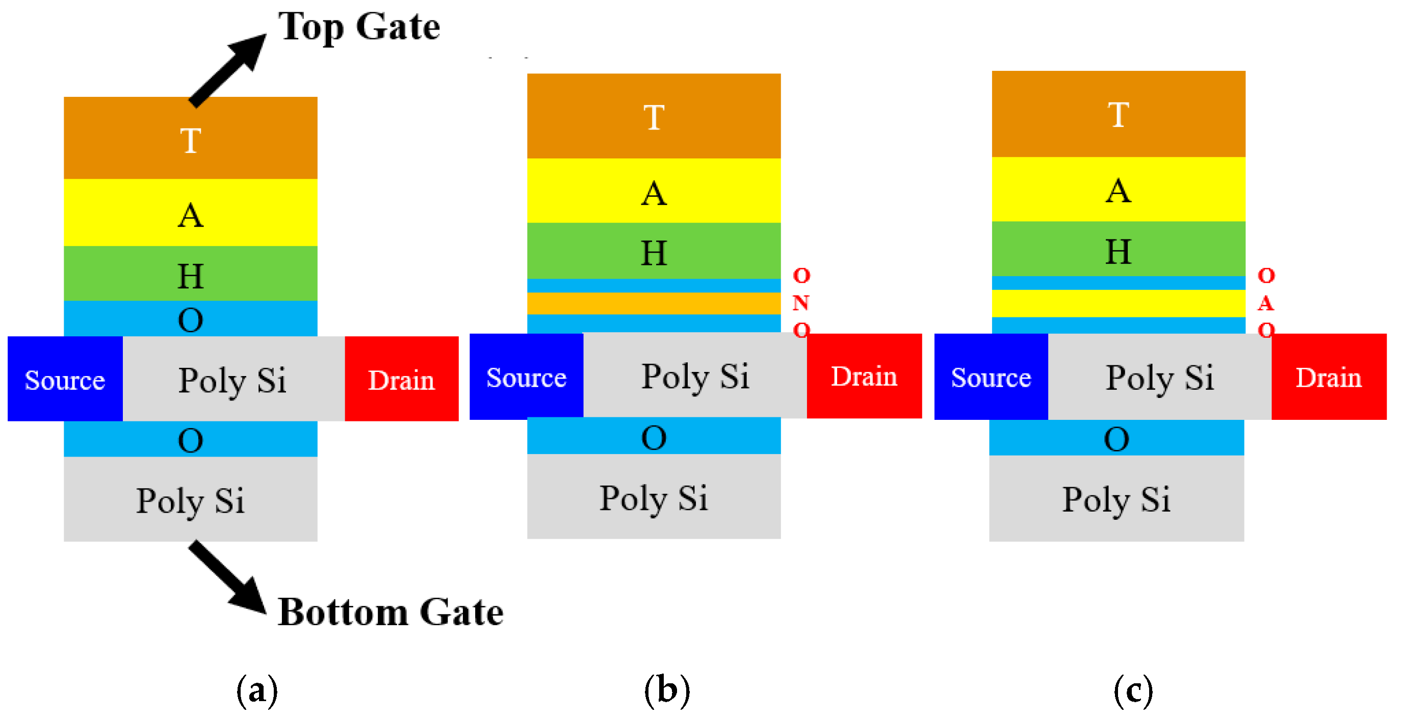
2.1. Structure of the Proposed Memory Device

In previous research, the advanced bandgap-engineered TaN/Al2O3/HfO2/SiO2/Si (BE-TAHOS) structure has been investigated for a faster erasing speed and larger memory window by incorporating Si3N4 at the tunneling oxide layer [37,38,39,40,41,42,43,44]. By utilizing this BE-TAHOS structure [34,35,36] and applying Al2O3 at the tunneling layer, the advanced structure of TaN/Al2O3/HfO2/SiO2/Al2O3/SiO2/Si (TAHOAOS) is designed for NOR flash memory.
Cross-sectional views of conventional TaN/Al2O3/HfO2/SiO2/Si (TAHOS), BE-TAHOS, and that of the proposed TAHOAOS structure are schematically shown in Figure 1. In order to compare the proposed TAHOAOS structure with not only conventional TAHOS but also the BE-TAHOS structure, BE-TAHOS is also designed with SiO2/Si3N4/SiO2 tunneling oxide layers [34,35,36]. The devices designed in this work have four terminals with top gate, bottom gate, source, and drain. The bottom gate is designed for solving disturbance issues.
Table 1 describes the film thickness and channel length for these devices. The simulated devices are composed of tunneling oxide layers with the same EOT of 3 nm for fair comparison. The blocking oxide is composed of 6 nm Al2O3, and CTL is composed of 4 nm HfO2. Bottom gate dielectric has a 3 nm thickness with SiO2. The length and thickness of the silicon channel are 40 nm and 12 nm, respectively. A gate-drain underlap (gate-source overlap) structure is applied for suppressing ambipolar current [38,39], which undesirably increases the off-state current. In specific, since the ambipolar current occurs due to band-to-band-tunneling (BTBT) current in the body/drain region, it is possible to suppress the ambipolar current by locating the gate far from the drain, which is called gate-drain underlap [38,39].

2.2. Model Physics and Model Parameters

To carefully investigate the electrical characteristics in these three different structures, tunneling models such as band-to-band-tunneling (BTBT), Fowler-Nordheim (FN) tunneling, direct tunneling, and trap-assisted tunneling (TAT) are applied in this device simulation with Synopsys Sentaurus™ through a technology computer-aided design (TCAD) tool. Physical models including Shockley-Read-Hall (SRH) recombination and E-field saturation models are also applied for precisely analyzing the memory operation.
For details, we adopted various mobility models including the PhuMob mobility model, Enormal (Lombardi) mobility model, and thin-layer mobility model to consider interfacial surface calibration roughness scattering and Coulomb scattering. In addition, models of eHighFieldSaturation, hHighFieldSaturation, and Avalanche (CarrierTempDrive) are used for reflecting velocity saturation and avalanche breakdown. Non-local mesh, eBarrierTunneling, and hBarrierTunneling are utilized for applying FN tunneling and direct tunneling.
In modeling HfO2 as CTL, charge trap density of 1.2 × 1020 cm3 is applied for HfO2, which corresponds to its charge trap density in memory device [9,10,11]. Specifically, the energy depth of electron is set as 0.7 eV from the lowest conduction band (LCB) of HfO2 [20], whereas the energy depth of hole is set as 2.9 eV from the highest valence band (HVB) [21] of HfO2. On the other hand, in modeling Al2O3, charge trap density of 2.0 × 1012 cm3 is applied, and the energy depth of electron/hole is set as 0.4/2.7 eV from LCB/HVB, respectively [8]. In addition, effective electron tunneling masses (meff) of 0.55 mo, 0.2 mo, and 0.4 mo are used in thin film of SiO2 [12], HfO2 [12], and Al2O3 [17], respectively.

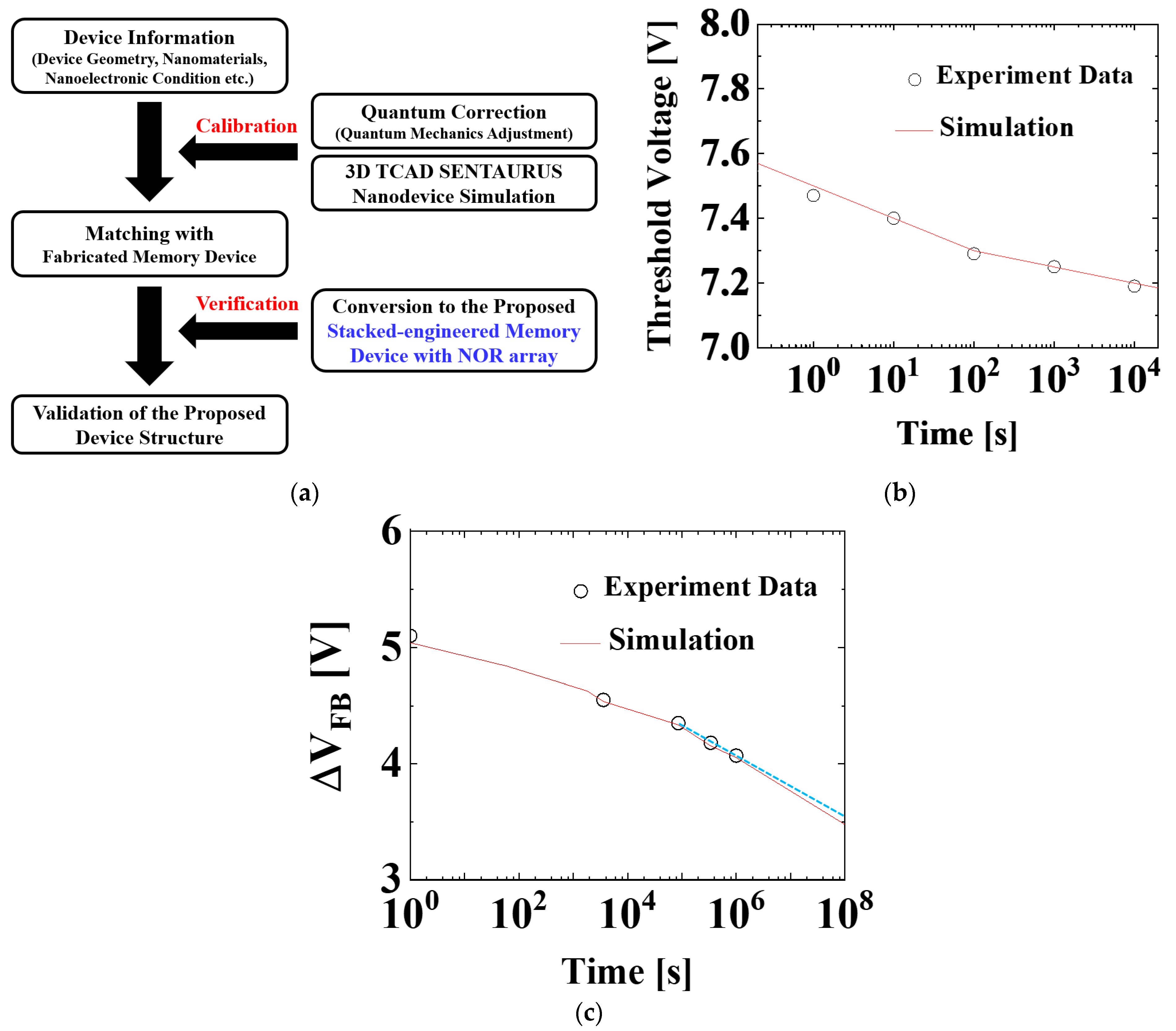
2.3. Workflow of Study and Calibration Process

Figure 2a illustrates the overall workflow of this paper. The calibration of memory device is performed with the fabricated memory devices [45,46], and then gate dielectric layers of SiO2/Al2O3/SiO2 is incorporated. Thereafter, validation of the proposed memory device structure is conducted in terms of retention characteristics and inhibition in the NOR flash array.
During the calibration process, quantum correlations are carefully conducted for IDS-IGS calibration, and retention calibration is performed under Synopsys Sentaurus™ three-dimensional (3D) TCAD simulation [47]. For details, we adopted various mobility models including the PhuMob mobility model, Enormal (Lombardi) mobility model, and thin-layer mobility model to consider interfacial surface calibration roughness scattering and Coulomb scattering. Firstly, IDS-IGS calibration is performed by carefully adopting the velocity saturation model, quantum model, and gate work function (WF). Secondly, retention characteristics are carefully calibrated with the fabricated memory devices. Figure 2b,c show our simulation results are well fit with the measured data of retention characteristics in the fabricated TaN/Al2O3/Si3N4/SiO2/Si (TANOS) device and BE-TAHOS device.

3. Results and Discussion

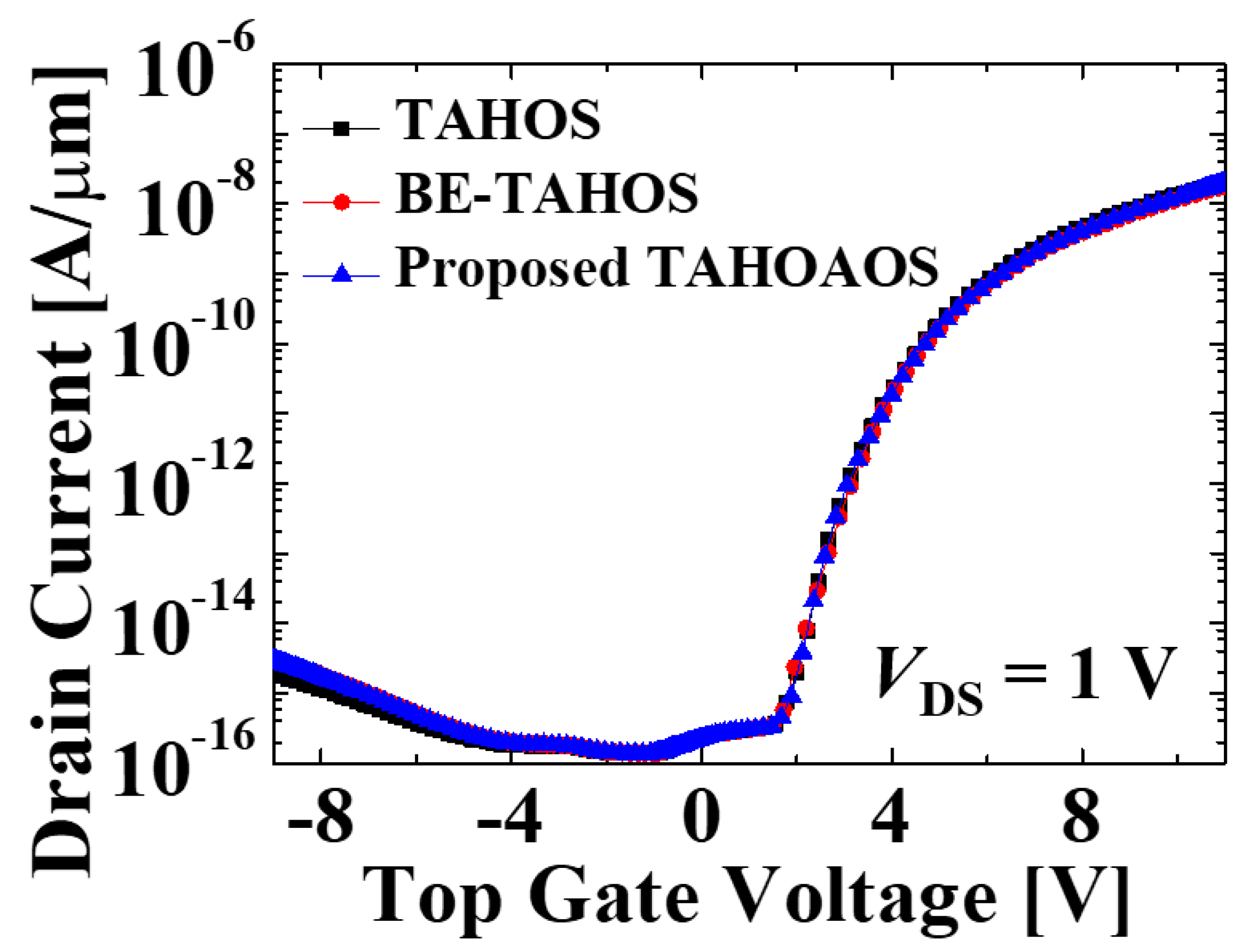
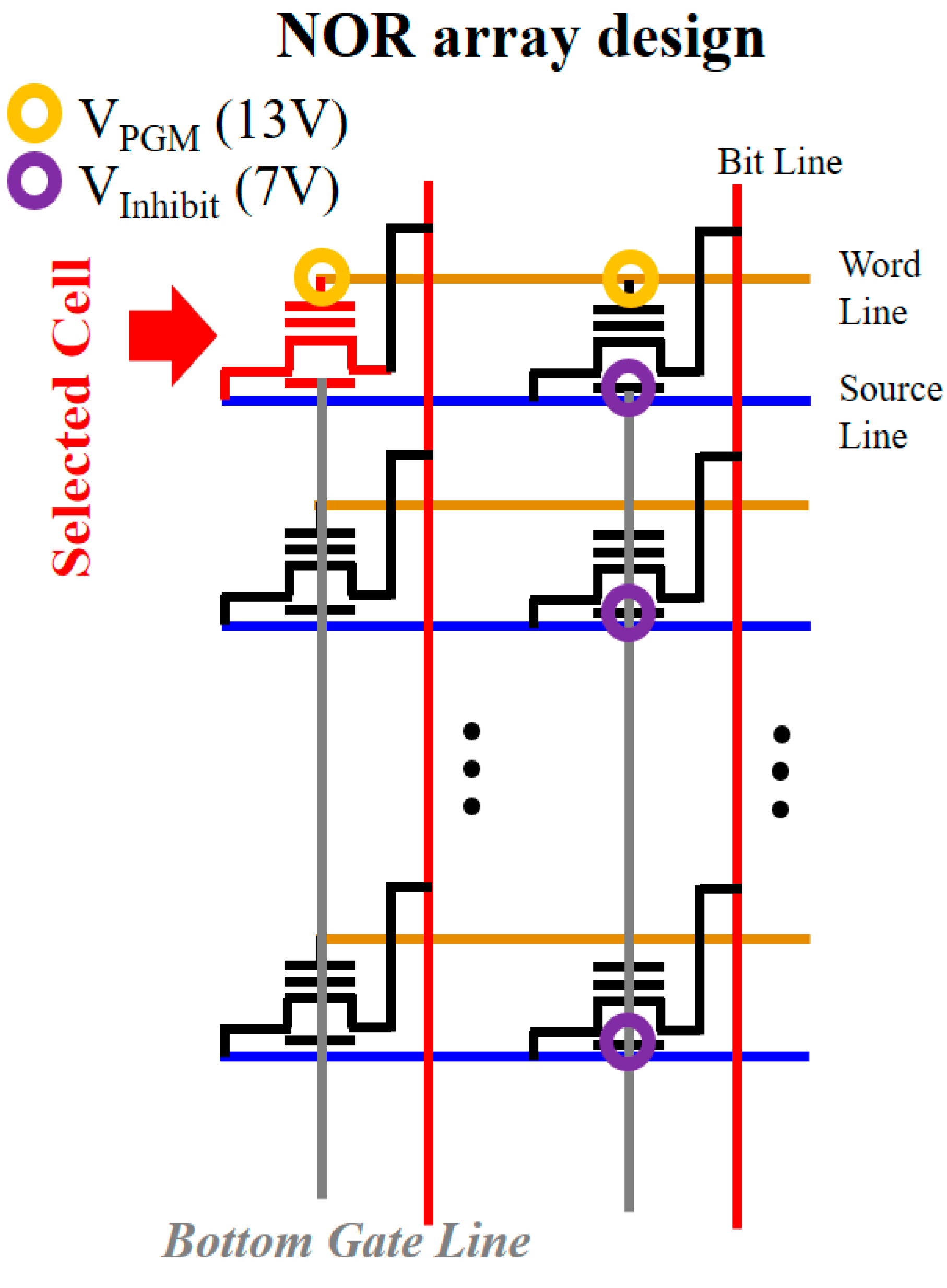
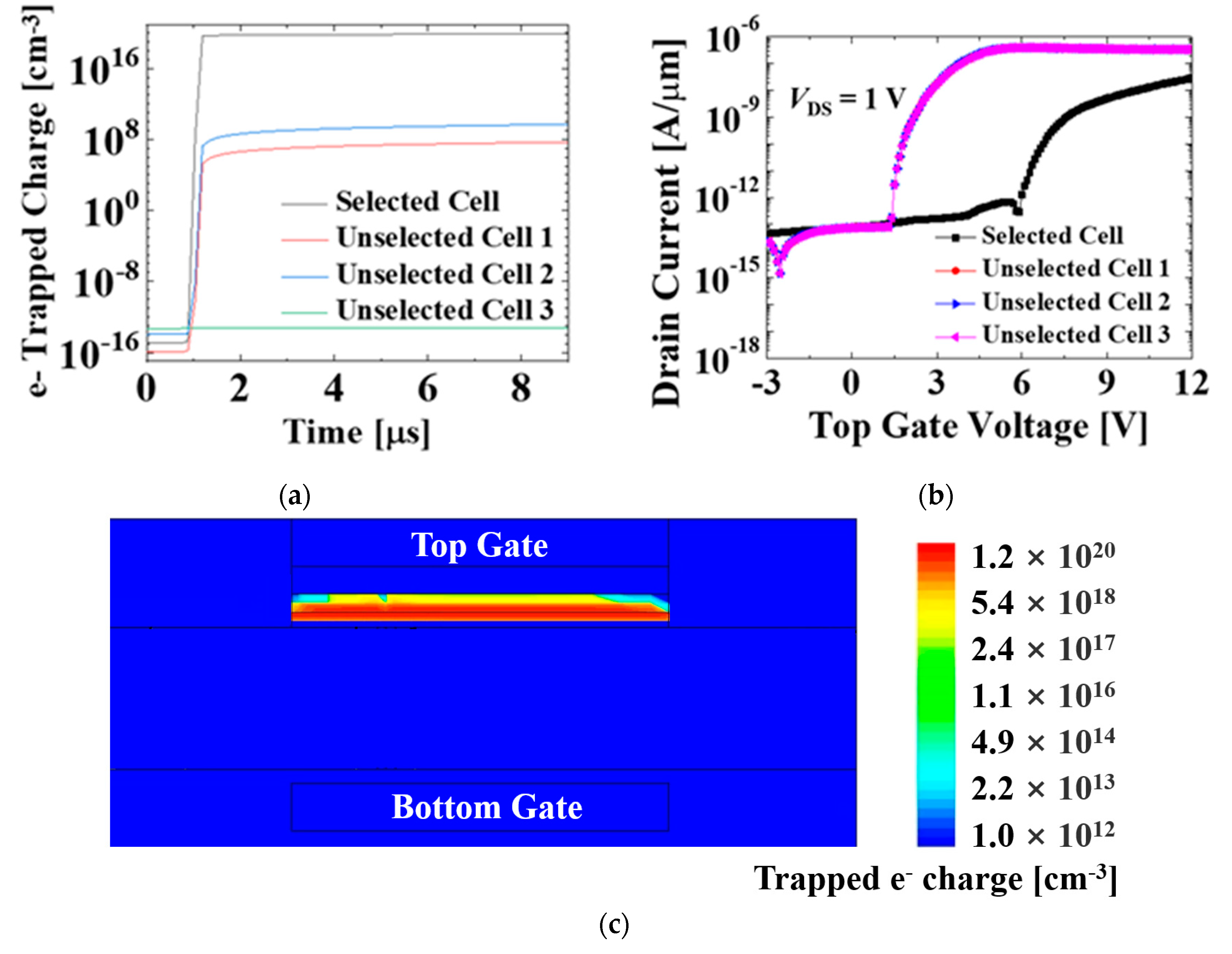
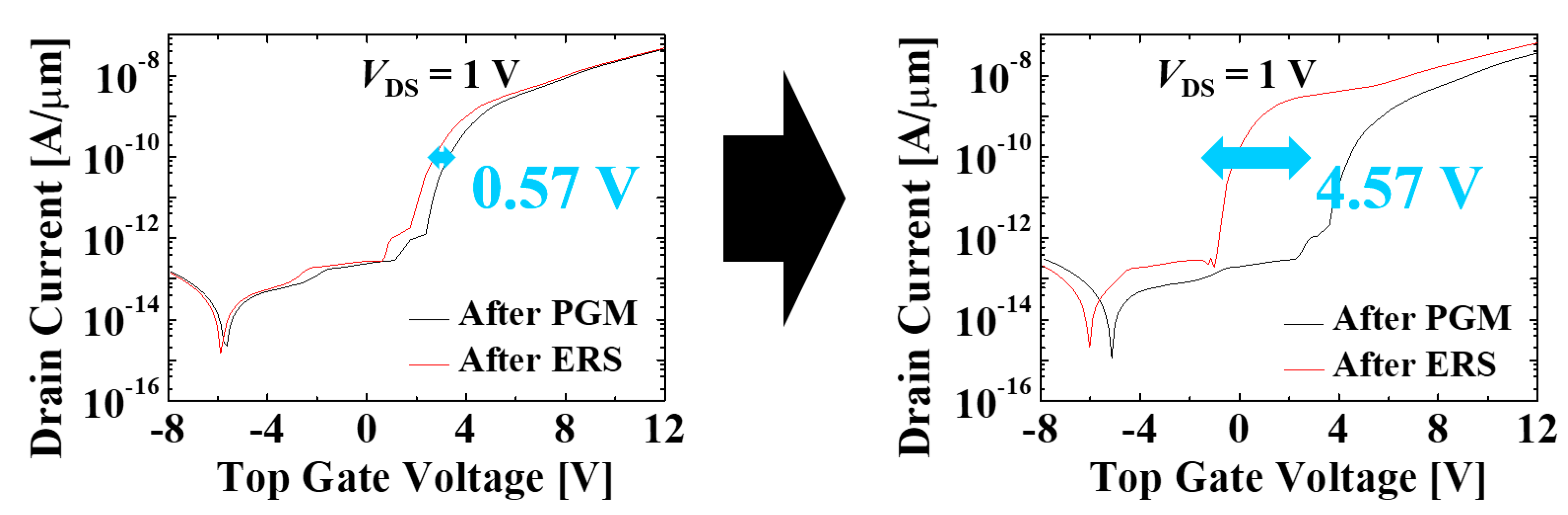
3.1. Demonstration of NOR Flash Array with the Proposed Memory Device Structure

Before demonstrating the retention enhancement from the proposed structure, the structure of the proposed memory device must be analyzed. In our proposed device structure, there are two major technological changes.
First, the tunneling oxide layer is technically changed for increasing physical thickness and maintaining the same EOT of 3 nm at the same time (the exact thicknesses are shown in Table 1). Since the EOT of the three structures is the same, the initial transfer characteristics are almost the same, as shown in Figure 3.
Second, the bottom gate was added to suppress programming of the unselected cell and solve disturbance issues [37]. Specifically, as illustrated in Figure 4, the additional bottom gates are connected with each other by the bottom gate line, which is perpendicular to the source line and word line. From this perpendicular design between the bottom gate line and word line, it is possible to program the selected cell only and inhibit programming of unselected cells, as described in the following paragraph.
For programming, the FN tunneling mechanism is used instead of the hot-carrier injection (HCI) mechanism, which has been widely adopted for the conventional programming method in the NOR flash array [48,49,50]. This is because the conventional HCI programming consumes significant power due to a significant drain current during programming [48]. On the other hand, FN programming can lower power consumption [37] due to its lower gate current compared to the higher drain current during HCI programming [48]. Therefore, FN tunneling is adopted for programming with low power consumption.
Table 2 describes the voltage applied in the selected cell and unselected cells during programming operation under the proposed NOR array design. Programming voltage (VPGM) of 13 V and inhibition voltage of 7 V are adopted, as only 13 V can program the memory cell in high-κ–based memory devices (namely, TAHOS structure) due to low EOT of dielectric layers [18,19,20,21].
The different voltages are applied to the top gate and bottom gate of each cell, which serves as selective programming without disturbance issues. Consequently, as demonstrated in Figure 5, only the selected cell is programmed by FN tunneling, whereas the unselected cells are not. Regarding threshold voltage (Figure 5b), all three unselected cells show nearly zero threshold voltage shift just after programming, whereas the selected sell shows significant threshold voltage shift just after programming. This is because more than 1016 cm3 trapped electron charge is needed for threshold voltage shift (Figure 5a,b) [18,19,20,21]. Therefore, it is possible to utilize our proposed structure in the NOR flash array without disturbance issues and increase the capacity of memory storage.

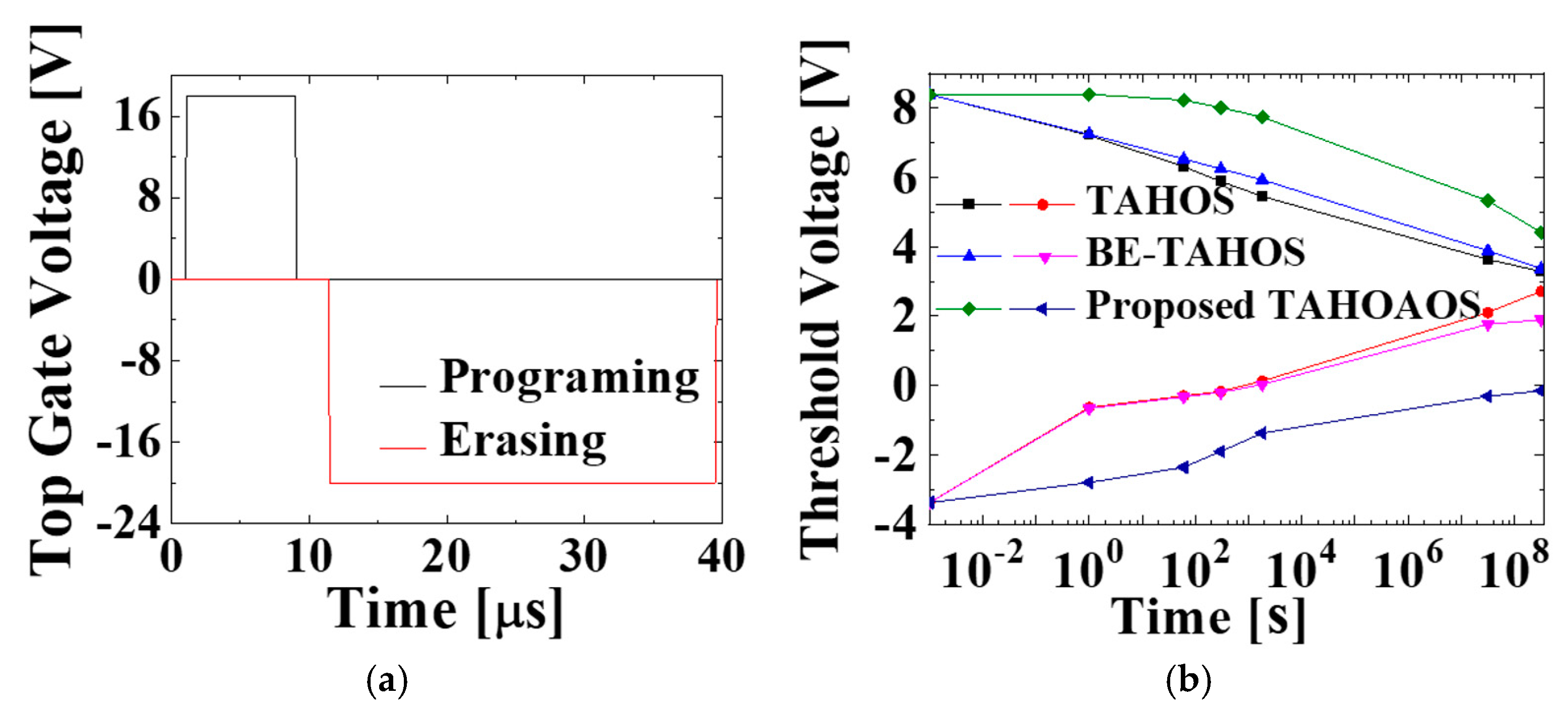
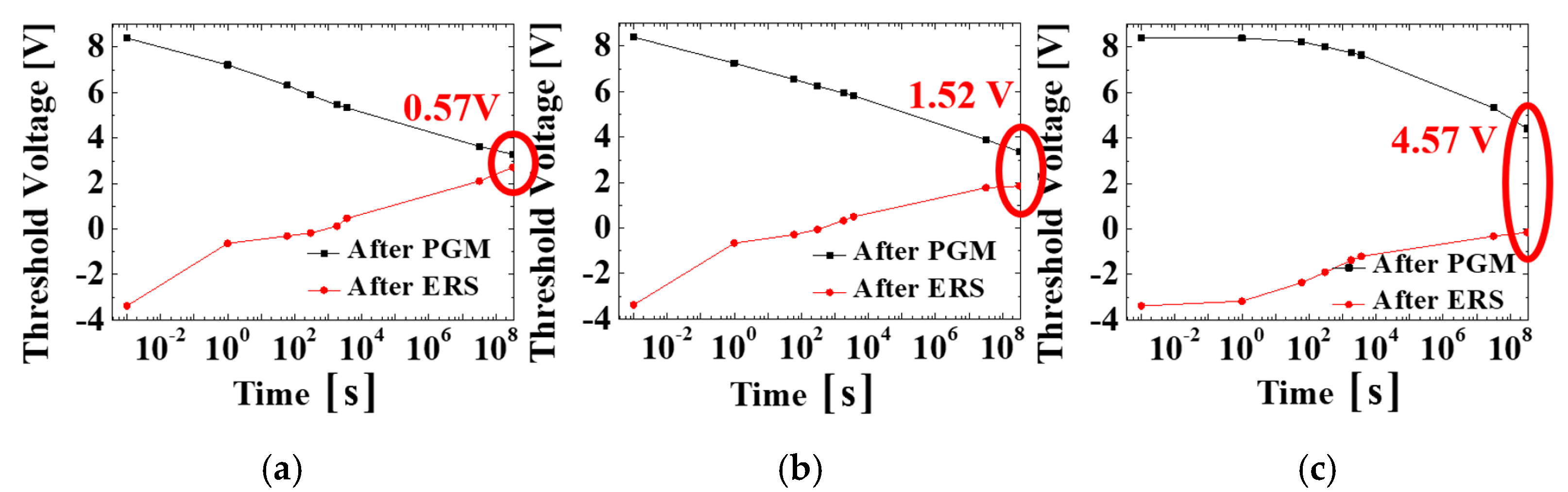
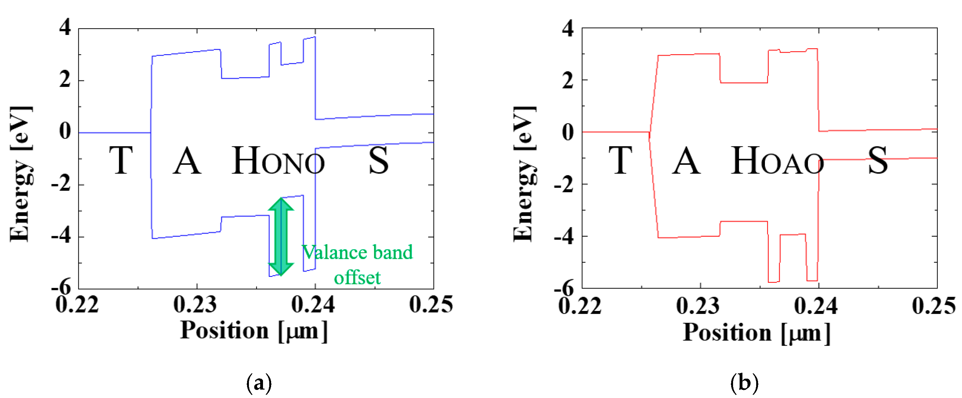
3.2. Retention Enhancement of the Proposed Memory Device Structure

In order to investigate the retention enhancement of the proposed TAHOAOS structure, devices with conventional TAHOS, and BE-TAHOS, proposed TAHOAOS structures are programmed and erased with top gate voltage as described in Figure 6a. Specifically, the high top gate voltage (17 V for programming and −21 V for erasing) is applied in order to perform a fair comparison by matching initial threshold voltage (namely, threshold voltage when time is 10−3 s). Then, retention characteristics of each structure are analyzed for 10 years. It is shown that our proposed TAHOAOS structure maintains a significant threshold voltage window for 10 years and is very strategic for retention characteristics, as demonstrated in Figure 6b.
Specifically, our proposed TAHOAOS structure maintains 4.57 V of the threshold voltage window, whereas conventional TAHOS structure only maintains 0.57 V after 10 years from programming and erasing (P/E) as illustrated in Figure 7. It is remarkable that our proposed TAHOAOS structure shows better retention characteristics (more than three times) compared to the BE-TAHOS structure.
However, there is one remarkable point in these retention characteristics. As shown in Figure 6b, the retention characteristics of conventional TAHOS and BE-TAHOS after erase operation (namely, red and pink line in Figure 6b) show barely little difference. Namely, even though retention characteristics of BE-TAHOS (pink line) is slightly better than that of conventional TAHOS (red line), the difference between them is reduced due to valence band offset.
This can be explained by energy band diagram. Figure 8 shows the energy band diagram of BE-TAHOS and the proposed TAHOAOS structure with reference to previous fabricated devices of the TAHOS and TANOS structure [51]. As illustrated in Figure 8a, substantial valence band offset exists in the BE-TAHOS structure. This valence band offset helps the hole to be ejected from HfO2 CTL. Therefore, the advantage of thicker tunneling oxide layers in BE-TAHOS (compared to conventional TAHOS) is reduced in terms of retention characteristics.
On the other hand, the proposed TAHOAOS structure has not only thicker tunneling oxide layers but also lower valance band offset compared to BE-TAHOS (Figure 8). Therefore, regarding hole retention, the proposed TAHOAOS structure has a remarkable competitive edge, as demonstrated in Figure 6b.
Figure 9 shows the transfer curves after 10 years of P/E operation in the conventional TAHOS structure and the proposed TAHOAOS structure. It is expected that our proposed structure can serve as a powerful tool for future big data markets with better reliability (retention), higher memory capacity, and low power operation (TFET-based memory [34,35,36,37,38,39,40]).
In summary, we have improved the retention characteristics with which HfO2-based nonvolatile charge-trapping memory has encountered [22,23,24,25], and opened up the possibility of practical application of HfO2-based NOR flash memory for better memory capacity.

3.3. Proposal for Future Research

We have proposed the design methodology for better retention characteristics and great immunity against disturbance issues by developing the TAHOAOS structure [37] on the NOR flash array. The proposed design technology is expected to improve the retention characteristics and decrease power consumption during programming (due to the programming method of FN tunneling) and during read operation (due to the TFET-based structure). Furthermore, it is expected that our newly proposed device structure with four terminals can solve the disturbance issue and make only a selected cell programmed.
However, even though our research has made considerable efforts to verify our proposed methodology, our research is basically limited to NOR flash application. We believe our proposed TAHOAOS structure can be applied beyond NOR flash application and to other fields such as 3D NAND flash and 3D AND flash. This is because our proposed technology may be applied in another domain by changing the design of the circuit. Therefore, we would like to suggest the future research topic to readers by analyzing our proposed technique in another array and another circuit design. It may be a desirable and interesting topic to develop our research with various future memory applications.

4. Conclusions

In this study, we propose the advanced structure for the NOR flash array with retention improvement. From the bottom gate effect, the disturbance issues are well suppressed, and it is possible to utilize the proposed structure in a NOR flash array. In addition, the threshold voltage window after 10 years of programming and erasing was considerably increased from 0.57 V to 4.57 V by incorporating Al2O3 in tunneling oxide layers. This enhancement is achieved by 1) high physical thickness of tunneling layers in the proposed structure (namely, high permittivity of Al2O3) and 2) lower valence band offset/conduction band offset in the proposed structure (namely, higher bandgap of Al2O3 compared to Si3N4). These results open up the possibility of using enriched CTL (HfO2) with improved retention characteristics. Therefore, the proposed TAHOAOS structure is very strategic for future highly integrated memory cells in big data markets with significant reliability enhancement.

Author Contributions

Writing—Original Draft & Data curation, Y.S.S.; Writing—Review & Editing, B.-G.P.; Validation, Y.S.S.; Supervision B.-G.P. All authors have read and agreed to the published version of the manuscript.

Funding

This work was supported by 2021 research fund of Korea Military Academy (Hwarangdae Research Institute).

Conflicts of Interest

The authors declare no conflict of interest.

References

  1. Imran, A.; Zoha, A.; Abu-Dayya, A. Challenges in 5G: How to empower SON with big data for enabling 5G. IEEE Netw. 2014, 28, 27–33. [Google Scholar] [CrossRef]
  2. Zheng, K.; Yang, Z.; Zhang, K.; Chatzimisios, P.; Yang, K.; Xiang, W. Big data-driven optimization for mobile networks toward 5G. IEEE Netw. 2016, 30, 44–51. [Google Scholar] [CrossRef]
  3. Han, Q.; Liang, S.; Zhang, H. Mobile cloud sensing, big data, and 5G networks make an intelligent and smart world. IEEE Netw. 2015, 29, 40–45. [Google Scholar] [CrossRef]
  4. Zhang, H.; Chen, G.; Ooi, B.C.; Tan, K.; Zhang, M. In-Memory Big Data Management and Processing: A Survey. IEEE Trans. Knowl. Data Eng. 2015, 27, 1920–1948. [Google Scholar] [CrossRef]
  5. Wang, Y.; Yu, H. An ultralow-power memory-based big-data computing platform by nonvolatile domain-wall nanowire devices. In Proceedings of the International Symposium on Low Power Electronics and Design (ISLPED), Beijing, China, 4–6 September 2013. [Google Scholar]
  6. Hamdioui, S.; Xie, L.; Anh Du Nguyen, H.; Taouil, M.; Bertles, K.; Corporaal, H.; Jiao, H.; Cathoor, F.; Wouters, D.; Eike, L.; et al. Memristor based computation-in-memory architecture for data-intensive applications. In Proceedings of the Design, Automation & Test in Europe Conference & Exhibition (DATE), Grenoble, France, 9–13 March 2015. [Google Scholar]
  7. Yoon, S.-M.; Lee, N.-Y.; Ryu, S.-O.; Choi, K.-J.; Park, Y.-S.; Lee, S.-Y.; Yu, B.-G.; Kang, M.-J.; Choi, S.-J.; Wuttig, M. Sb-Se-based phase-change memory device with lower power and higher speed operations. IEEE Electron. Device Lett. 2006, 27, 445–447. [Google Scholar] [CrossRef]
  8. Marcon, D.; Van Hove, M.; De Jaeger, B.; Posthuma, N.; Wellekens, D.; You, S.; Kang, X.; Wu, T.-L.; Willems, M.; Stoffels, S.; et al. Direct comparison of GaN-based e-mode architectures (recessed MISHEMT and p-GaN HEMTs) processed on 200 mm GaN-on-Si with Au-free technology. In Proceedings of the SPIE 9363, Gallium Nitride Materials and Devices X, San Francisco, CA, USA, 13 March 2015. [Google Scholar]
  9. Zhu, W.J.; Ma, T.P.; Zafar, S.; Tamagawa, T. Charge trapping in ultrathin hafnium oxide. IEEE Electron. Device Lett. 2002, 23, 597–599. [Google Scholar] [CrossRef]
  10. Zou, X.; Jin, L.; Yan, L.; Zhang, Y.; Ai, D.; Zhao, C.; Xu, F.; Li, C.; Huo, Z. The influence of grain boundary interface traps on electrical characteristics of top select gate transistor in 3D NAND flash memory. Solid State Electron. 2019, 153, 67–73. [Google Scholar] [CrossRef]
  11. Yao, Y.; Li, C.; Huo, Z.L.; Liu, M.; Zhu, C.X.; Gu, C.Z.; Duan, X.F.; Wang, Y.G.; Gu, L.; Yu, R.C. In situ electron holography study of charge distribution in high-κ charge-trapping memory. Nat. Commun. 2013, 4, 1–8. [Google Scholar] [CrossRef]
  12. Hinkle, C.L.; Fulton, C.; Nemanich, R.J.; Lucovsky, G. A novel approach for determining the effective tunneling mass of electrons in HfO2 and other high-K alternative gate dielectrics for advanced CMOS devices. Microelectron. Eng. 2004, 72, 257–262. [Google Scholar] [CrossRef]
  13. Ali, T.; Polakowski, P.; Riedel, S.; Büttner, T.; Kämpfe, T.; Rudolph, M.; Pätzold, B.; Seidel, K.; Löhr, D.; Hoffmann, R.; et al. High Endurance Ferroelectric Hafnium Oxide-Based FeFET Memory Without Retention Penalty. IEEE Trans. Electron. Devices 2018, 65, 3769–3774. [Google Scholar] [CrossRef]
  14. Lee, B.H.; Kang, L.; Qi, W.J.; Nieh, R.; Jeon, Y.; Onishi, K.; Lee, J.C. Ultrathin hafnium oxide with low leakage and excellent reliability for alternative gate dielectric application. In Proceedings of the International Electron Devices Meeting (IEDM), Washington, DC, USA, 5–8 December 1999. [Google Scholar]
  15. Choi, Y.; Lee, K.; Kim, K.Y.; Kim, S.; Lee, J.; Lee, R.; Kim, H.-M.; Song, Y.S.; Kim, S.; Lee, J.-H.; et al. Simulation of the effect of parasitic channel height on characteristics of stacked gate-all-around nanosheet FET. Solid State Electron. 2020, 164, 107686. [Google Scholar] [CrossRef]
  16. Kim, J.H.; Kim, H.W.; Song, Y.S.; Kim, S.; Kim, G. Analysis of Current Variation with Work Function Variation in L-Shaped Tunnel-Field Effect Transistor. Micromachines 2020, 11, 780. [Google Scholar] [CrossRef] [PubMed]
  17. Molina-Reyes, J.; Uribe-Vargas, H.; Torres-Torres, R.; Mani-Gonzalez, P.G.; Herrera-Gomez, A. Accurate modeling of gate tunneling currents in Metal-Insulator-Semiconductor capacitors based on ultra-thin atomic-layer deposited Al2O3 and post-metallization annealing. Thin Solid Film. 2017, 638, 48–56. [Google Scholar] [CrossRef]
  18. Xu, W.C.; He, H.X.; Jing, X.S.; Wu, S.J.; Zhang, Z.; Gao, J.W.; Gao, X.S.; Zhou, G.F.; Lu, X.B.; Liu, J.-M. High performance organic nonvolatile memory transistors based on HfO2 and poly(α-methylstyrene) electret hybrid charge-trapping layers. Appl. Phys. Lett. 2017, 111, 1–5. [Google Scholar] [CrossRef]
  19. You, H.-C.; Kuo, P.-Y.; Ko, F.-H.; Chao, T.-S.; Lei, T.-F. The Impact of Deep Ni Salicidation and hbox NH3 Plasma Treatment on Nano-SOI FinFETs. IEEE Electron. Device Lett. 2006, 27, 799–801. [Google Scholar] [CrossRef]
  20. Driussi, F.; Spiga, S.; Lamperti, A.; Congedo, G.; Gambi, A. Simulation Study of the Trapping Properties of HfO2-Based Charge-Trap Memory Cells. IEEE Trans. Electron. Devices 2014, 61, 2056–2063. [Google Scholar] [CrossRef]
  21. Zhang, Y.; Shao, Y.Y.; Lu, X.B.; Zeng, M.; Zhang, Z.; Gao, X.S.; Zhang, X.J.; Liu, J.-M.; Dai, J.Y. Defect states and charge trapping characteristics of HfO2 films for high performance nonvolatile memory applications. Appl. Phys. Lett. 2014, 105, 172902. [Google Scholar] [CrossRef] [Green Version]
  22. Stesmans, A.; Afanasev, V.V. Defect correlated with positive charge trapping in functional HfO2 layers on (100)Si revealed by electron spin resonance: Evidence for oxygen vacancy? Microelectron. Eng. 2017, 178, 112–115. [Google Scholar] [CrossRef]
  23. Chen, Y.Y.; Goux, L.; Clima, S.; Govoreanu, B.; Degraeve, R.; Sankar Kar, G.; Fantini, A.; Groesenken, G.; Wouters, D.J.; Jurczak, M.; et al. Endurance/Retention Trade-off on HfO2/Metal Cap 1T1R Bipolar RRAM. IEEE Trans. Electron. Devices 2013, 60, 1114–1121. [Google Scholar] [CrossRef]
  24. Mitrovic, I.Z.; Luy, Y.; Buiu, O.; Hall, S. Current transport mechanisms in HfO2xSiO21-x/SiO2gate stacks. Microelectron. Eng. 2007, 84, 2306–2309. [Google Scholar] [CrossRef]
  25. Cerbu, F.; Madia, O.; Andreev, D.V.; Fadida, S.; Eizenberg, M.; Breuil, L.; Lisoni, J.G.; Kittl, J.A.; Strand, J.; Shluger, A.L.; et al. Intrinsic electron traps in atomic-layer deposited HfO2 insulators. Appl. Phys. Lett. 2016, 108, 1–5. [Google Scholar] [CrossRef]
  26. Bersuker, G.; Sim, J.H.; Park, C.S.; Young, C.D.; Nadkarni, S.V.; Choi, R.; Lee, H.B. Mechanism of Electron Trapping and Characteristics of Traps in HfO2 Gate Stacks. IEEE Trans. Device Mater. Reliab. 2007, 7, 138–145. [Google Scholar] [CrossRef]
  27. Khosla, R.; Rolseth, E.G.; Kumar, P.; Vadakupudhupalayam, S.S.; Sharma, S.K.; Schulze, J. Charge Trapping Analysis of Metal/Al2O3/SiO2/Si, Gate Stack for Emerging Embedded Memories. IEEE Trans. Device Mater. Reliab. 2017, 17, 80–89. [Google Scholar] [CrossRef]
  28. Xu, Z.; Huo, Z.; Zhu, C.; Cui, Y.; Wang, M.; Zheng, Z.; Liu, J.; Wang, Y.; Li, F.; Liu, M. Performance-improved nonvolatile memory with aluminum nanocrystals embedded in Al2O3 for high temperature applications. J. Appl. Phys. 2011, 110, 1–5. [Google Scholar] [CrossRef]
  29. Gu, S.-H.; Hsu, C.-W.; Wang, T.; Lu, W.-P.; Ku, Y.-H.J.; Lu, C.-Y. Numerical Simulation of Bottom Oxide Thickness Effect on Charge Retention in SONOS Flash Memory Cells. IEEE Trans. Electron. Devices 2006, 54, 90–97. [Google Scholar] [CrossRef] [Green Version]
  30. King, Y.-C.; Liu, T.-J.K.; Hu, C. A long-refresh dynamic/quasi-nonvolatile memory device with 2-nm tunneling oxide. IEEE Electron. Device Lett. 1999, 20, 409–411. [Google Scholar] [CrossRef]
  31. Hanafi, H.; Tiwari, S.; Khan, I. Fast and long retention-time nano-crystal memory. IEEE Trans. Electron. Devices 1996, 43, 1553–1558. [Google Scholar] [CrossRef]
  32. Malavena, G.; Spinelli, A.S.; Compagnoni, C.M. Implementing Spike-Timing-Dependent Plasticity and Unsupervised Learning in a Mainstream NOR Flash Memory Array. In Proceedings of the 2018 IEEE International Electron Devices Meeting (IEDM), San Francisco, CA, USA, 1–5 December 2018; pp. 1–4. [Google Scholar]
  33. Malavena, G.; Filippi, M.; Spinelli, A.S.; Compagnoni, C.M. Unsupervised Learning by Spike-Timing-Dependent Plasticity in a Mainstream NOR Flash Memory Array—Part I: Cell Operation. IEEE Trans. Electron. Devices 2019, 66, 4727–4732. [Google Scholar] [CrossRef]
  34. Lue, H.-T.; Wang, S.Z.; Lai, E.-K.; Shih, Y.-H.; Lai, S.-C.; Yang, L.-W.; Chen, K.-C.; Ku, J.; Hsieh, K.-Y.; Liu, R.; et al. BE-SONOS: A bandgap engineered SONOS with excellent performance and reliability. In Proceedings of the IEEE International Electron Devices Meeting, Washington, DC, USA, 5 December 2005. [Google Scholar]
  35. Lue, H.-T.; Wang, S.-Y.; Lai, E.-K.; Hsieh, K.-Y.; Liu, R.; Lu, C.Y. A BE-SONOS (Bandgap Engineered SONOS) NAND for Post-Floating Gate Era Flash Memory. In Proceedings of the 2007 International Symposium on VLSI Technology, Systems and Applications (VLSI-TSA), Hsinchu, Taiwan, 23–25 April 2007; pp. 1–2. [Google Scholar]
  36. Hsu, T.-H.; Lue, H.T.; King, Y.-C.; Hsieh, J.-Y.; Lai, E.-K.; Hsieh, K.-Y.; Liu, R.; Lu, C.-Y. A High-Performance Body-Tied FinFET Bandgap Engineered SONOS (BE-SONOS) for nand-Type Flash Memory. IEEE Electron. Device Lett. 2007, 28, 443–445. [Google Scholar] [CrossRef]
  37. Song, Y.S.; Jang, T.; Min, K.K.; Baek, M.-H.; Yu, J.; Kim, Y.; Lee, J.-H.; Park, B.-G. Tunneling oxide engineering for improving retention in nonvolatile charge-trapping memory with TaN/Al2O3/HfO2/SiO2/Al2O3/SiO2/Si structure. Jpn. J. Appl. Phys. 2020, 59, 61006. [Google Scholar] [CrossRef]
  38. Khatami, Y.; Banerjee, K. Steep Subthreshold Slope n- and p-Type Tunnel-FET Devices for Low-Power and Energy-Efficient Digital Circuits. IEEE Trans. Electron. Devices 2009, 56, 2752–2761. [Google Scholar] [CrossRef]
  39. Yu, J.; Kim, S.; Baek, M.-H.; Min, K.K.; Jang, T.; Song, Y.S.; Park, B.G. Investigation of Ambipolar Current Suppression Using Dual Work Function Metal Gate in L-Shaped Tunnel Field Effect Transistor. In Proceedings of the IEIE Summer Conference, Jeju-do, Korea, 26–28 June 2019. [Google Scholar]
  40. Kim, Y.; Kim, T.; Beak, M.H.; Jang, T.; Song, Y.S.; Jeon, B.; Park, B.G. An Area Efficient Adaptive Neuron Circuit Exploiting Tunnel Field-Effect Transistor. In Proceedings of the IEIE Summer Conference, Jeju-do, Korea, 26–28 June 2019. [Google Scholar]
  41. Tripathy, M.R.; Singh, A.K.; Samad, A.; Chander, S.; Baral, K.; Singh, P.K.; Jit, S. Device and Circuit-Level Assessment of GaSb/Si Heterojunction Vertical Tunnel-FET for Low-Power Applications. IEEE Trans. Electron. Devices 2020, 67, 1285–1292. [Google Scholar] [CrossRef]
  42. Kim, T.; Park, K.; Jang, T.; Baek, M.-H.; Song, Y.S.; Park, B.-G. Input-modulating adaptive neuron circuit employing asymmetric floating-gate MOSFET with two independent control gates. Solid State Electron. 2020, 163, 107667. [Google Scholar] [CrossRef]
  43. Kim, T.; Song, Y.S.; Park, B.-G. Overflow Handling Integrate-and-Fire Silicon-on-Insulator Neuron Circuit Incorporating a Schmitt Trigger Implemented by Back-Gate Effect. J. Nanosci. Nanotechnol. 2019, 19, 6183–6186. [Google Scholar] [CrossRef]
  44. Song, Y.S.; Kim, J.H.; Kim, G.; Kim, H.-M.; Kim, S.; Park, B.-G. Improvement in Self-Heating Characteristic by Incorporating Hetero-Gate-Dielectric in Gate-All-Around MOSFETs. IEEE J. Electron. Devices Soc. 2021, 9, 36–41. [Google Scholar] [CrossRef]
  45. Park, H.; Bersuker, G.; Gilmer, D.; Lim, K.Y.; Jo, M.; Hwang, H.; Padovani, A.; Larcher, L.; Pavan, P.; Taylor, W.; et al. Charge loss in TANOS devices caused by Vt sensing measurements during retention. In Proceedings of the 2010 IEEE International Memory Workshop, Seoul, Korea, 16–19 May 2010; pp. 1–2. [Google Scholar] [CrossRef]
  46. Congedo, G.; Lamperti, A.; Salicio, O.; Spiga, S. Multi-Layered Al2O3/HfO2/SiO2/Si3N4/SiO2 Thin Dielectrics for Charge Trap Memory Applications. ECS J. Solid State Sci. Technol. 2013, 2, N1–N5. [Google Scholar] [CrossRef]
  47. Synopsys Inc. Version K-2015.06-SP; Synopsys Inc.: Mountain View, CA, USA, 2017. [Google Scholar]
  48. Della Marca, V.; Postel-Pellerin, J.; Just, G.; Canet, P.; Ogier, J.-L. Impact of endurance degradation on the programming efficiency and the energy consumption of NOR flash memories. Microelectron. Reliab. 2014, 54, 2262–2265. [Google Scholar] [CrossRef]
  49. Compagnoni, C.M.; Chiavarone, L.; Calabrese, M.; Ghidotti, M.; Lacaita, A.L.; Spinelli, A.S.; Visconti, A. Fundamental Limitations to the Width of the Programmed VTVT Distribution of nor Flash Memories. IEEE Trans. Electron. Devices 2010, 57, 1761–1767. [Google Scholar] [CrossRef]
  50. Choi, S.-J.; Han, J.-W.; Kim, S.; Moon, D.-I.; Jang, M.-G.; Kim, J.S.; Kim, K.H.; Lee, G.S.; Oh, J.S.; Song, M.H.; et al. Performance Breakthrough in NOR Flash Memory with Dopant-Segregated Schottky-Barrier (DSSB) SONOS Devices. In Proceedings of the 2009 Symposium on VLSI Technology, Kyoto, Japan, 15–17 June 2009. [Google Scholar]
  51. Spiga, S.; Congedo, G.; Russo, U.; Lamperti, A.; Salicio, O.; Driussi, F.; Vianello, E. Experimental and simulation study of the program efficiency of HfO2 based charge trapping memories. In Proceedings of the 2010 European Solid State Device Research Conference, Sevila, Spain, 14–16 September 2010; pp. 408–411. [Google Scholar]
Figure 1. Schematic view illustrating (a) conventional TaN/Al2O3/HfO2/SiO2/Si (TAHOS), (b) bandgap engineered (BE)-TAHOS, and (c) proposed TaN/Al2O3/HfO2/SiO2/Al2O3/SiO2/Si (TAHOAOS) structure with two gate terminals. All structures commonly have HfO2 as charge-trapping layer (CTL) and Al2O3 as blocking oxide. The abbreviated letters T, A, H, O, N stand for tantalum nitride (TaN, gate metal), Al2O3, HfO2, SiO2, Si3N4, respectively.
Micromachines 12 00328 g001
Figure 2. (a) Illustration that summarizes overall workflow of this paper; (b) calibration results based on the fabricated TANOS device [45]; (c) another calibration result based on fabricated BE-TAHOS device [46]. (Sky blue dot line indicates the linear approximation of retention characteristic in the fabricated BE-TAHOS device.).
Micromachines 12 00328 g002
Figure 3. Basic transfer characteristics of three different device structures. These transfer characteristics show that our simulation is well designed with the same EOT thickness.
Micromachines 12 00328 g003
Figure 4. NOR array design for the proposed memory device structure. The newly added bottom gate line is perpendicular to the word line for selective programming.
Micromachines 12 00328 g004
Figure 5. (a) Change of electron charge trap density during programming at the cells of the proposed NOR array design. The density of trapped electron charge becomes saturated due to limited top gate voltage. In the selected cell, the higher top gate voltage may increase the saturated density of the trapped electron charge; (b) transfer characteristics just after programming of the cells in the proposed NOR array design; (c) cross-sectional view of the selected cell with TAHOS structure that illustrates the distribution of the trapped electron charge after programming.
Micromachines 12 00328 g005
Figure 6. (a) Top gate bias during programming and erasing, and (b) retention characteristics of the conventional TAHOS, BE-TAHOS, and the proposed TAHOAOS structure. The high top gate voltage (17 V for programming and −21 V for erasing) is applied in order to perform fair comparison by matching initial threshold voltage at 1 micro-second. (Specifically, programming with top gate voltage of 13 V, as in Table 2, results in different initial threshold voltage [37], and hence programming with a higher top gate voltage of 17 V is performed for fair comparison.).
Micromachines 12 00328 g006
Figure 7. Detailed description of retention characteristics in (a) conventional TAHOS, (b) BE-TAHOS, and (c) proposed TAHOAOS structure.
Micromachines 12 00328 g007
Figure 8. Energy band diagram of (a) BE-TAHOS, and (b) proposed TAHOAOS structure. Regarding retention characteristics, the valence band offset of BE-TAHOS (green arrow in panel a) mitigates the advantage of thicker tunneling oxide layers in BE-TAHOS. The abbreviated letters T, A, H, O, N stand for tantalum nitride (TaN, gate metal), Al2O3, HfO2, SiO2, Si3N4, respectively.
Micromachines 12 00328 g008
Figure 9. Enhancement of retention characteristics by the proposed tunneling oxide engineering. The graphs are calculated after 10 years of programming and erasing.
Micromachines 12 00328 g009
Table 1. Film thickness and channel length in conventional TAHOS, BE-TAHOS, and proposed TAHOAOS structure.
RegionMaterialThickness (nm)
Tunneling oxideSiO23
SiO2/Si3N4/SiO21/1.7/1
SiO2/Al2O3/SiO21/2.3/1
Blocking oxideAl2O36
Charge-trapping layerHfO24
Bottom gate dielectricSiO23
Channel (length)Si40
Channel (thickness)Si12
Table 2. The voltage applied in the selected cell and unselected cells during programming with the proposed NOR array design.
Cell TypeTop Gate Voltage (V)Bottom Gate Voltage (V)
Selected cell130
Unselected cell 1137
Unselected cell 207
Unselected cell 300
Publisher’s Note: MDPI stays neutral with regard to jurisdictional claims in published maps and institutional affiliations.

