
Batch Transfer Printing of Small-Size Silicon Nano-Films with Flat Stamp

 , , , and
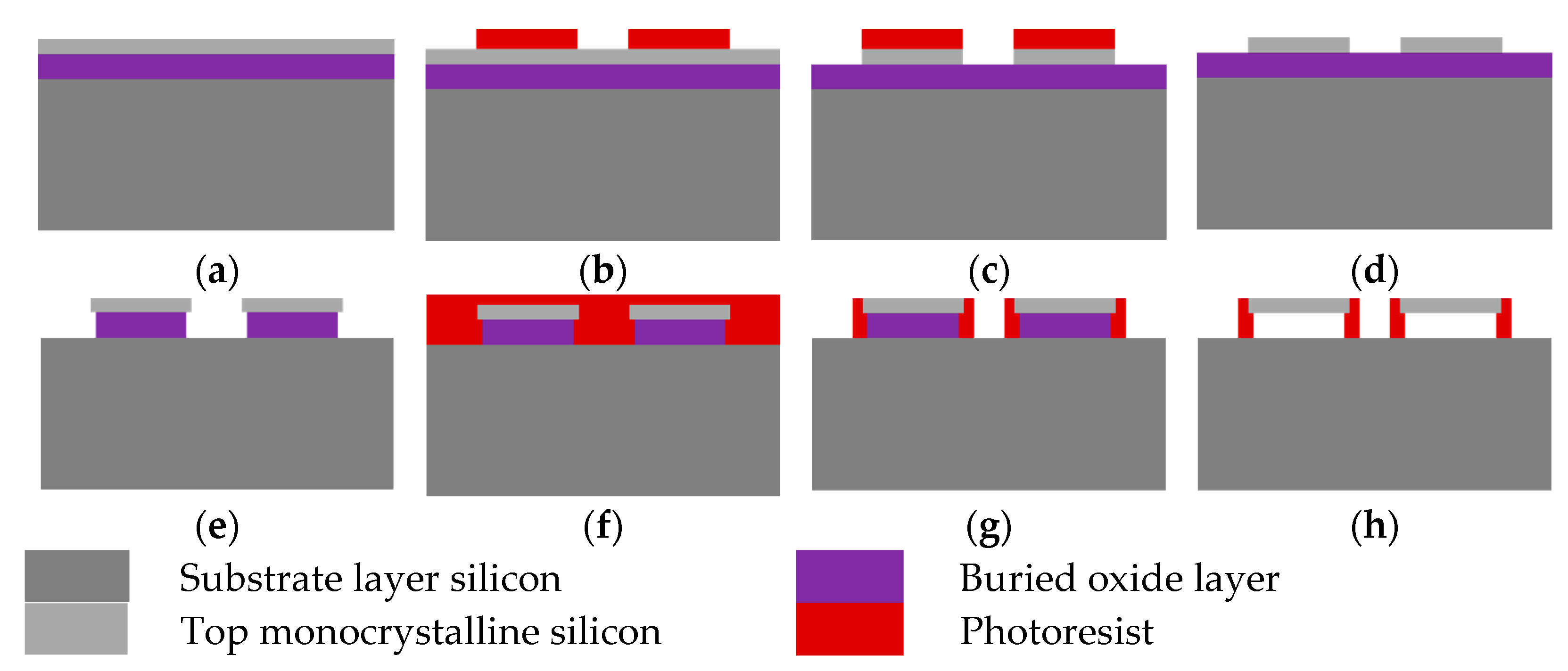
Abstract
:1. Introduction
2. Result and Discussion
2.1. Principle of Transfer Printing
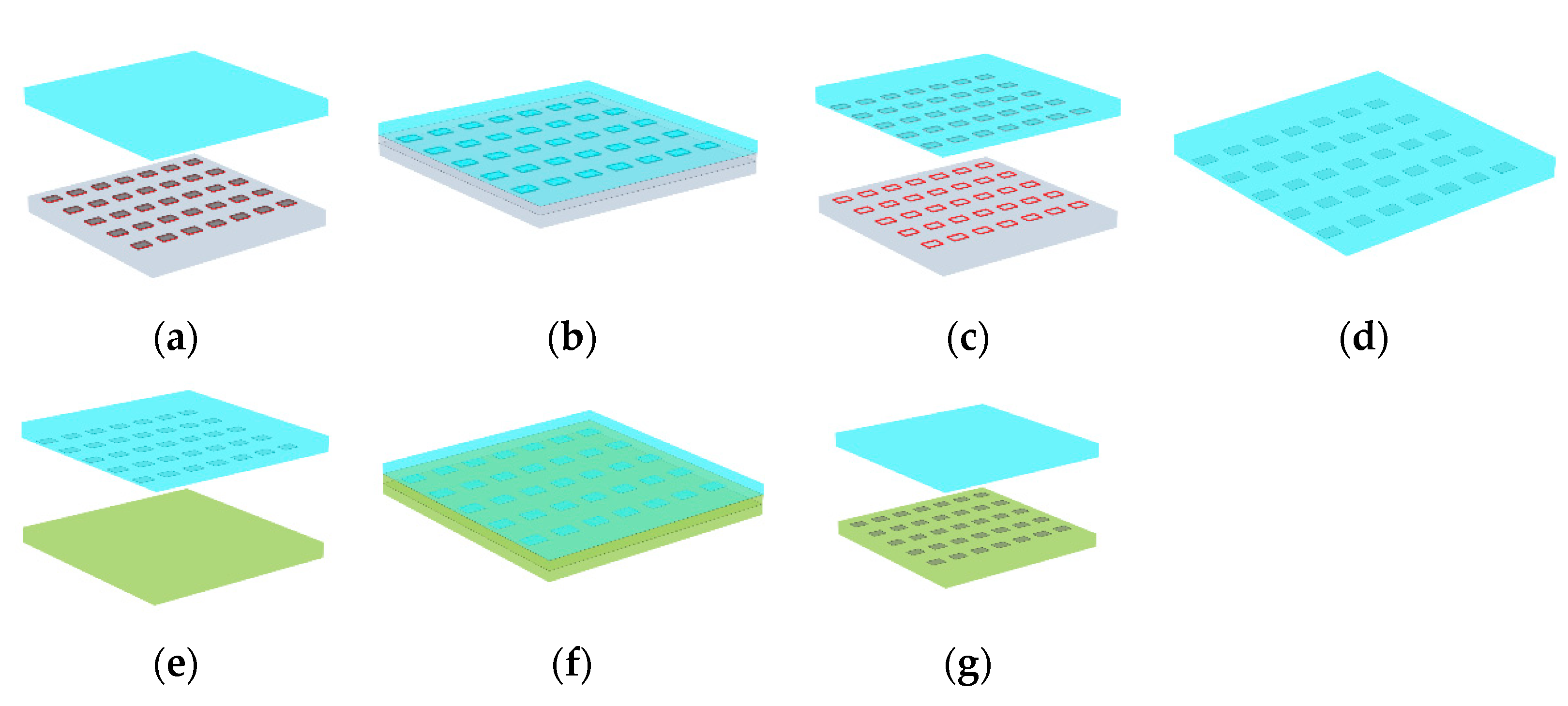
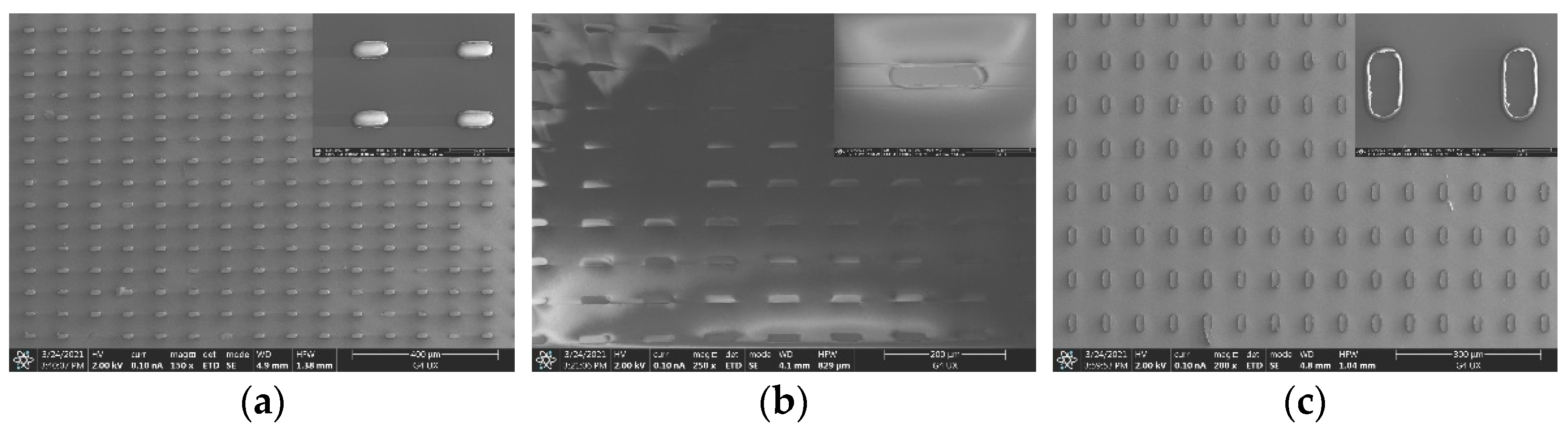
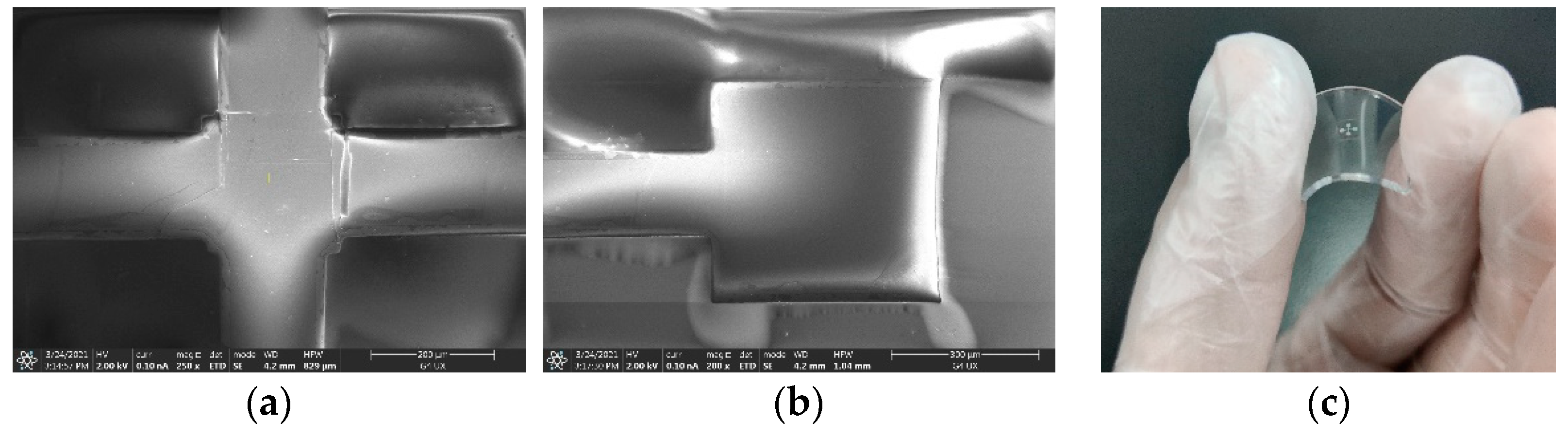
2.2. Transfer Printing Process
3. Materials and Methods
3.1. Fabrication of Silicon Nano-Film Structure
3.2. Fabrication of Stamp and Receiving Substrate
3.3. Transfer Printing
4. Conclusions
Author Contributions
Funding
Conflicts of Interest
References
- Lee, S.; Franklin, S.; Hassani, F.A.; Yokota, T.; Nayeem, O.G.; Wang, Y.; Leib, R.; Cheng, G.; Franklin, D.W.; Someya, T. Nanomesh pressure sensor for monitoring finger manipulation without sensory interference. Science 2020, 370, 966–970. [Google Scholar] [CrossRef] [PubMed]
- Bai, H.; Li, S.; Barreiros, J.; Tu, Y.; Pollock, C.R.; Shepherd, R.F. Stretchable distributed fiber-optic sensors. Science 2020, 370, 848–852. [Google Scholar] [CrossRef] [PubMed]
- You, I.; Mackanic, D.G.; Matsuhisa, N.; Kang, J.; Kwon, J.; Beker, L.; Mun, J.; Suh, W.; Kim, T.Y.; Tok, J.B.H.; et al. Artificial multimodal receptors based on ion relaxation dynamics. Science 2020, 370, 961–965. [Google Scholar] [CrossRef] [PubMed]
- Gu, L.; Poddar, S.; Lin, Y.; Long, Z.; Zhang, D.; Zhang, Q.; Shu, L.; Qiu, X.; Kam, M.; Javey, A.; et al. A biomimetic eye with a hemispherical perovskite nanowire array retina. Nature 2020, 581, 278–282. [Google Scholar] [CrossRef] [PubMed]
- Araromi, O.A.; Graule, M.A.; Dorsey, K.L.; Castellanos, S.; Foster, J.R.; Hsu, W.-H.; Passy, A.E.; Vlassak, J.J.; Weaver, J.C.; Walsh, C.J.; et al. Ultra-sensitive and resilient compliant strain gauges for soft machines. Nature 2020, 587, 219–224. [Google Scholar] [CrossRef] [PubMed]
- Fuentes-Hernandez, C.; Chou, W.-F.; Khan, T.M.; Diniz, L.; Lukens, J.; Larrain, F.A.; Rodriguez-Toro, V.A.; Kippelen, B. Large-area low-noise flexible organic photodiodes for detecting faint visible light. Science 2020, 370, 698–701. [Google Scholar] [CrossRef] [PubMed]
- Kim, H.J.; Chen, B.; Suo, Z.; Hayward, R.C. Ionoelastomer junctions between polymer networks of fixed anions and cations. Science 2020, 367, 773–776. [Google Scholar] [CrossRef] [PubMed]
- Liu, X.; Gao, H.; Ward, J.E.; Liu, X.; Yin, B.; Fu, T.; Chen, J.; Lovley, D.R.; Yao, J. Power generation from ambient humidity using protein nanowires. Nature 2020, 578, 550–554. [Google Scholar] [CrossRef] [PubMed]
- Rogers, J.A.; Lagally, M.G.; Nuzzo, R.G. Synthesis, assembly and applications of semiconductor nanomembranes. Nature 2011, 477, 45–53. [Google Scholar] [CrossRef] [PubMed]
- Zhao, H.B.; Li, K.; Han, M.D.; Zhu, F.; Vazquez-Guardado, A.; Guo, P.J.; Xie, Z.Q.; Park, Y.; Chen, L.; Wang, X.J.; et al. Buckling and twisting of advanced materials into morphable 3D mesostructures. Proc. Natl. Acad. Sci. USA 2019, 116, 13239–13248. [Google Scholar] [CrossRef] [PubMed] [Green Version]
- Khang, D.Y.; Jiang, H.Q.; Huang, Y.; Rogers, J.A. A stretchable form of single-crystal silicon for high-performance electronics on rubber substrates. Science 2006, 311, 208–212. [Google Scholar] [CrossRef] [PubMed] [Green Version]
- Wang, R.X.; Liu, Y.; Xu, W.; Bai, B.; Zhang, G.J.; Liu, J.; Xiong, J.J.; Zhang, W.D.; Xue, C.Y.; Zhang, B.Z. A ‘fitness-wheel-shaped’ MEMS vector hydrophone for 3D spatial acoustic orientation. J. Micromech. Microeng. 2017, 27, 8. [Google Scholar] [CrossRef]
- Lee, K.J.; Motala, M.J.; Meitl, M.A.; Childs, W.R.; Menard, E.; Shim, A.K.; Rogers, J.A.; Nuzzo, R.G. Large-Area, Selective Transfer of Microstructured Silicon: A Printing-Based Approach to High-Performance Thin-Film Transistors Supported on Flexible Substrates. Adv. Mater. 2005, 17, 2332–2336. [Google Scholar] [CrossRef]
- Meitl, M.A.; Zhu, Z.T.; Kumar, V.; Lee, K.J.; Feng, X.; Huang, Y.Y.; Adesida, I.; Nuzzo, R.G.; Rogers, J.A. Transfer printing by kinetic control of adhesion to an elastomeric stamp. Nat. Mater. 2006, 5, 33–38. [Google Scholar] [CrossRef]
- Park, S.I.; Xiong, Y.; Kim, R.H.; Elvikis, P.; Meitl, M.; Kim, D.H.; Wu, J.; Yoon, J.; Yu, C.J.; Liu, Z.J.S. Printed Assemblies of Inorganic Light-Emitting Diodes for Deformable and Semitransparent Displays. Science 2009, 325, 977–981. [Google Scholar] [CrossRef] [PubMed] [Green Version]
- Kim, S.; Wu, J.A.; Carlson, A.; Jin, S.H.; Kovalsky, A.; Glass, P.; Liu, Z.J.; Ahmed, N.; Elgan, S.L.; Chen, W.Q.; et al. Microstructured elastomeric surfaces with reversible adhesion and examples of their use in deterministic assembly by transfer printing. Proc. Natl. Acad. Sci. USA 2010, 107, 17095–17100. [Google Scholar] [CrossRef] [PubMed] [Green Version]
- Yang, Y.; Hwang, Y.; Cho, H.A.; Song, J.-H.; Park, S.-J.; Rogers, J.A.; Ko, H.C. Arrays of Silicon Micro/Nanostructures Formed in Suspended Configurations for Deterministic Assembly Using Flat and Roller-Type Stamps. Small 2011, 7, 484–491. [Google Scholar] [CrossRef] [PubMed]
- Xu, S.; Yan, Z.; Jang, K.I.; Huang, W.; Fu, H.R.; Kim, J.; Wei, Z.; Flavin, M.; McCracken, J.; Wang, R.; et al. Assembly of micro/nanomaterials into complex, three-dimensional architectures by compressive buckling. Science 2015, 347, 154–159. [Google Scholar] [CrossRef] [PubMed] [Green Version]
- Wang, R.; Shen, W.; Zhang, W.; Song, J.; Li, N.; Liu, M.; Zhang, G.; Xue, C.; Zhang, W. Design and implementation of a jellyfish otolith-inspired MEMS vector hydrophone for low-frequency detection. Microsyst. Nanoeng. 2021, 7, 1. [Google Scholar] [CrossRef] [PubMed]
- Wu, J.; Dan, Q.; Liu, S. Effect of viscoelasticity of PDMS on transfer printing. In Proceedings of the International Conference on Electronic Packaging Technology, Changsha, China, 11–14 August 2015. [Google Scholar]
- Liu, J.; Pang, B.; Xue, R.; Li, R.; Song, J.; Zhao, X.; Wang, D.; Hu, X.; Lu, Y.; Wang, L. Sacrificial layer-assisted nanoscale transfer printing. Microsyst. Nanoeng. 2020, 6, 80. [Google Scholar] [CrossRef] [PubMed]


Publisher’s Note: MDPI stays neutral with regard to jurisdictional claims in published maps and institutional affiliations. |
© 2021 by the authors. Licensee MDPI, Basel, Switzerland. This article is an open access article distributed under the terms and conditions of the Creative Commons Attribution (CC BY) license (https://creativecommons.org/licenses/by/4.0/).
Share and Cite
Cao, W.; Liu, G.; Miao, J.; Zhang, G.; Cui, J.; Yang, Y.; He, C.; Zhang, W.; Wang, R. Batch Transfer Printing of Small-Size Silicon Nano-Films with Flat Stamp. Micromachines 2021, 12, 1255. https://doi.org/10.3390/mi12101255
Cao W, Liu G, Miao J, Zhang G, Cui J, Yang Y, He C, Zhang W, Wang R. Batch Transfer Printing of Small-Size Silicon Nano-Films with Flat Stamp. Micromachines. 2021; 12(10):1255. https://doi.org/10.3390/mi12101255
Chicago/Turabian StyleCao, Wenping, Guochang Liu, Jinwei Miao, Guojun Zhang, Jiangong Cui, Yuhua Yang, Changde He, Wendong Zhang, and Renxin Wang. 2021. "Batch Transfer Printing of Small-Size Silicon Nano-Films with Flat Stamp" Micromachines 12, no. 10: 1255. https://doi.org/10.3390/mi12101255