Thermal and Photo Sensing Capabilities of Mono- and Few-Layer Thick Transition Metal Dichalcogenides


Abstract
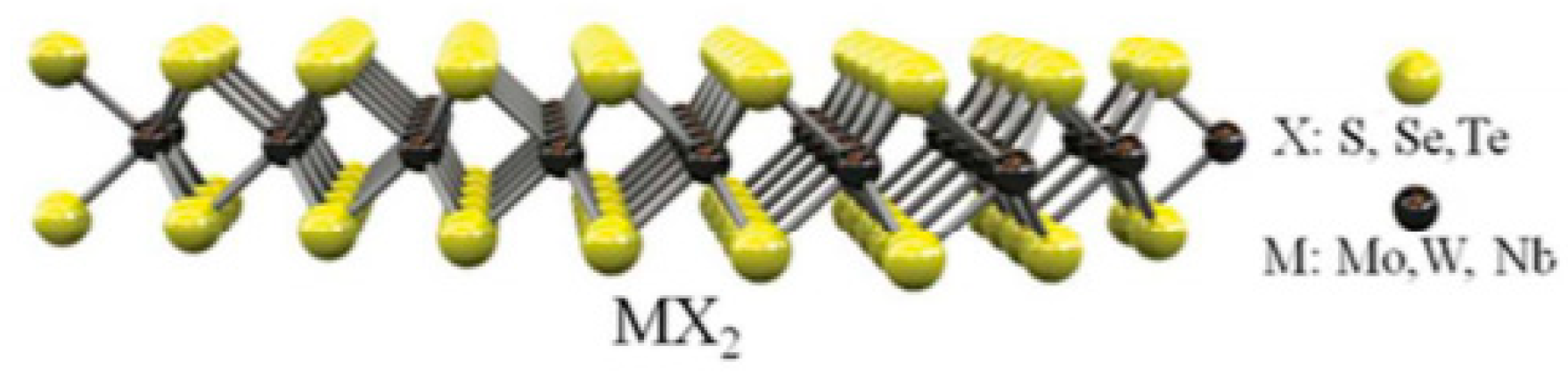
:1. Introduction
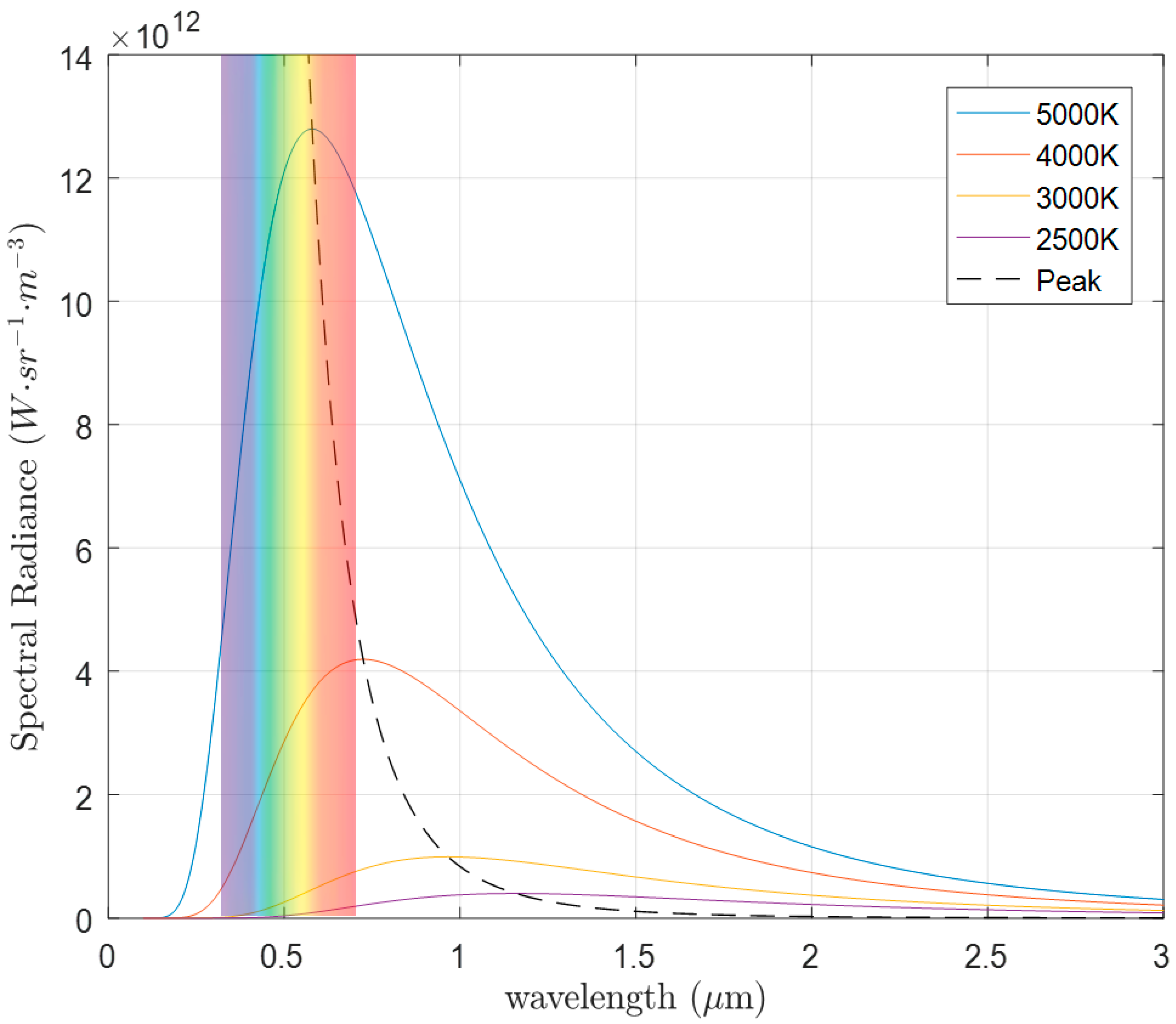
2. Theory
2.1. Non-Contact
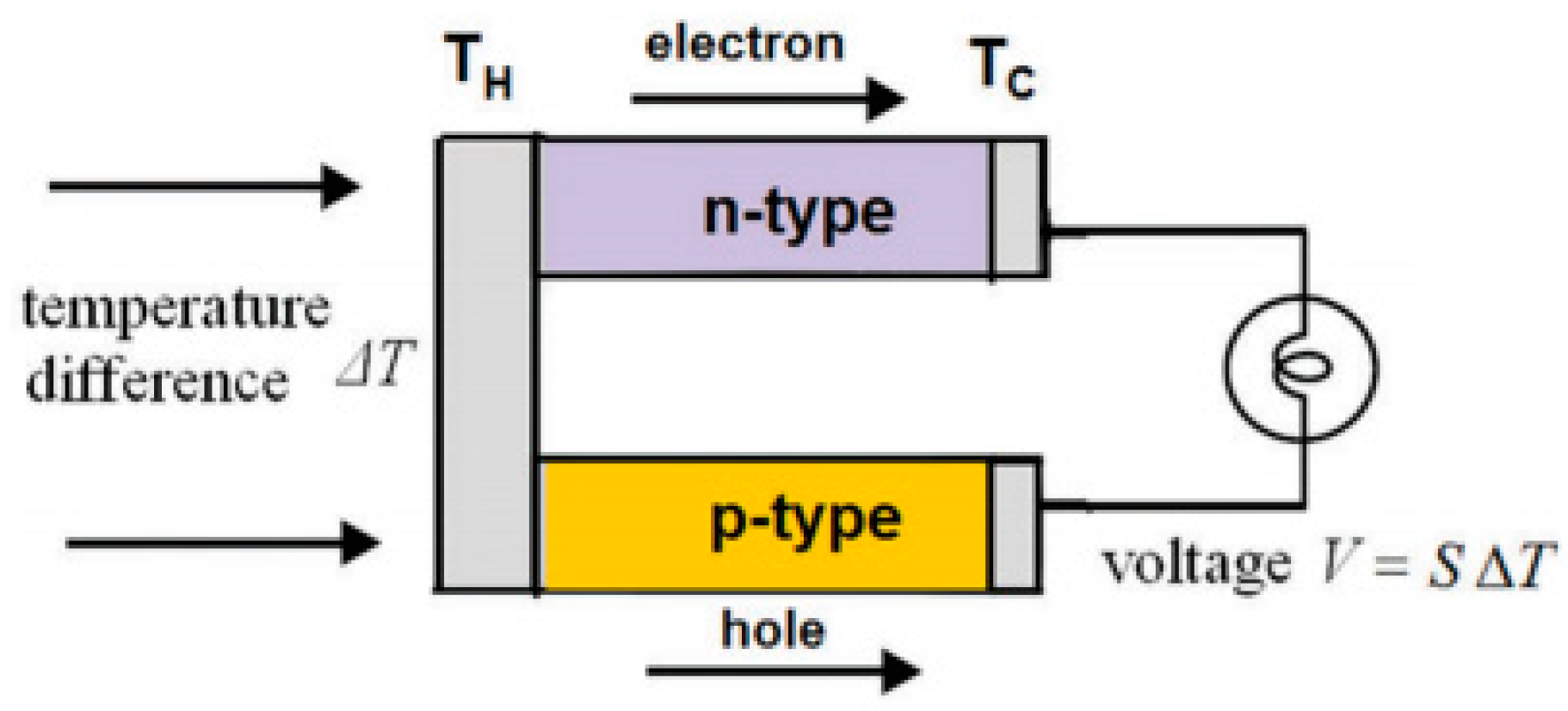
2.2. Contact
3. TMD-Based Photodetectors
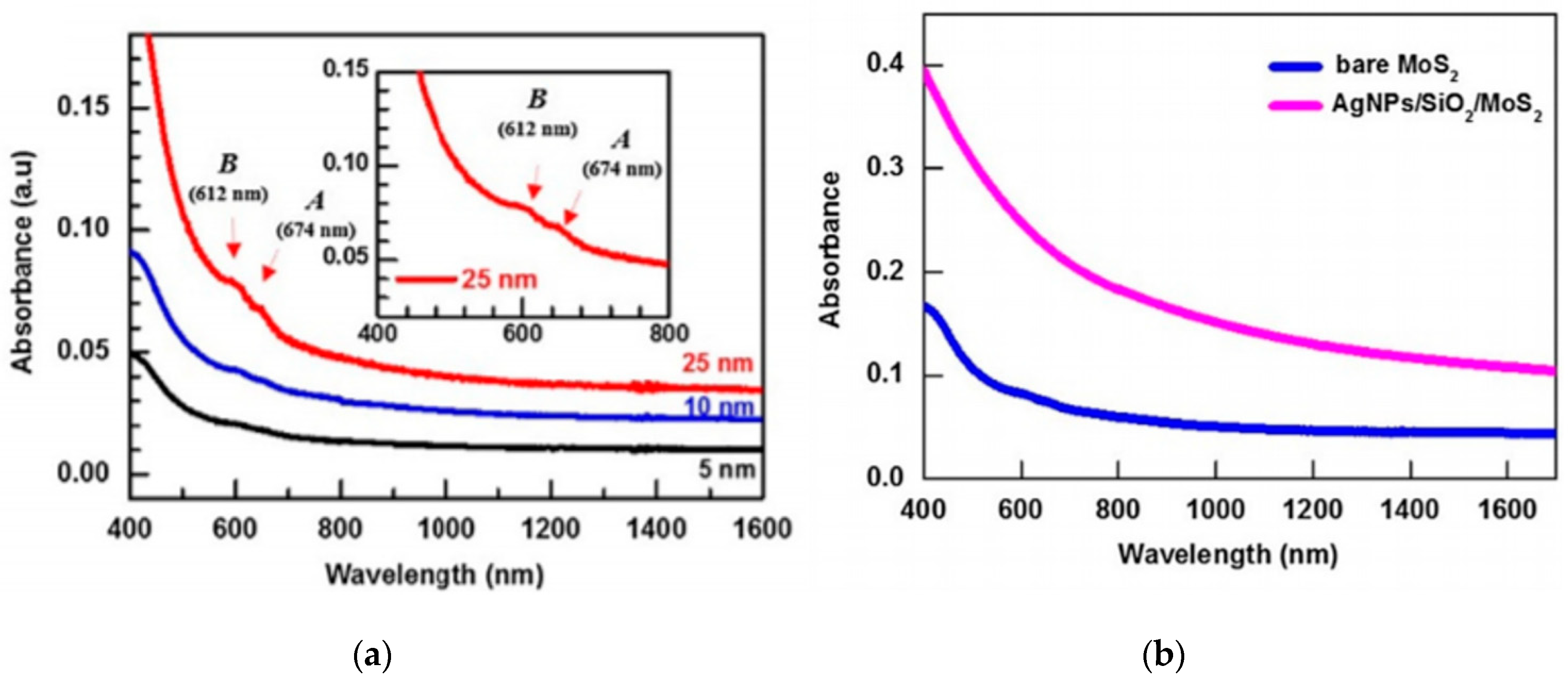
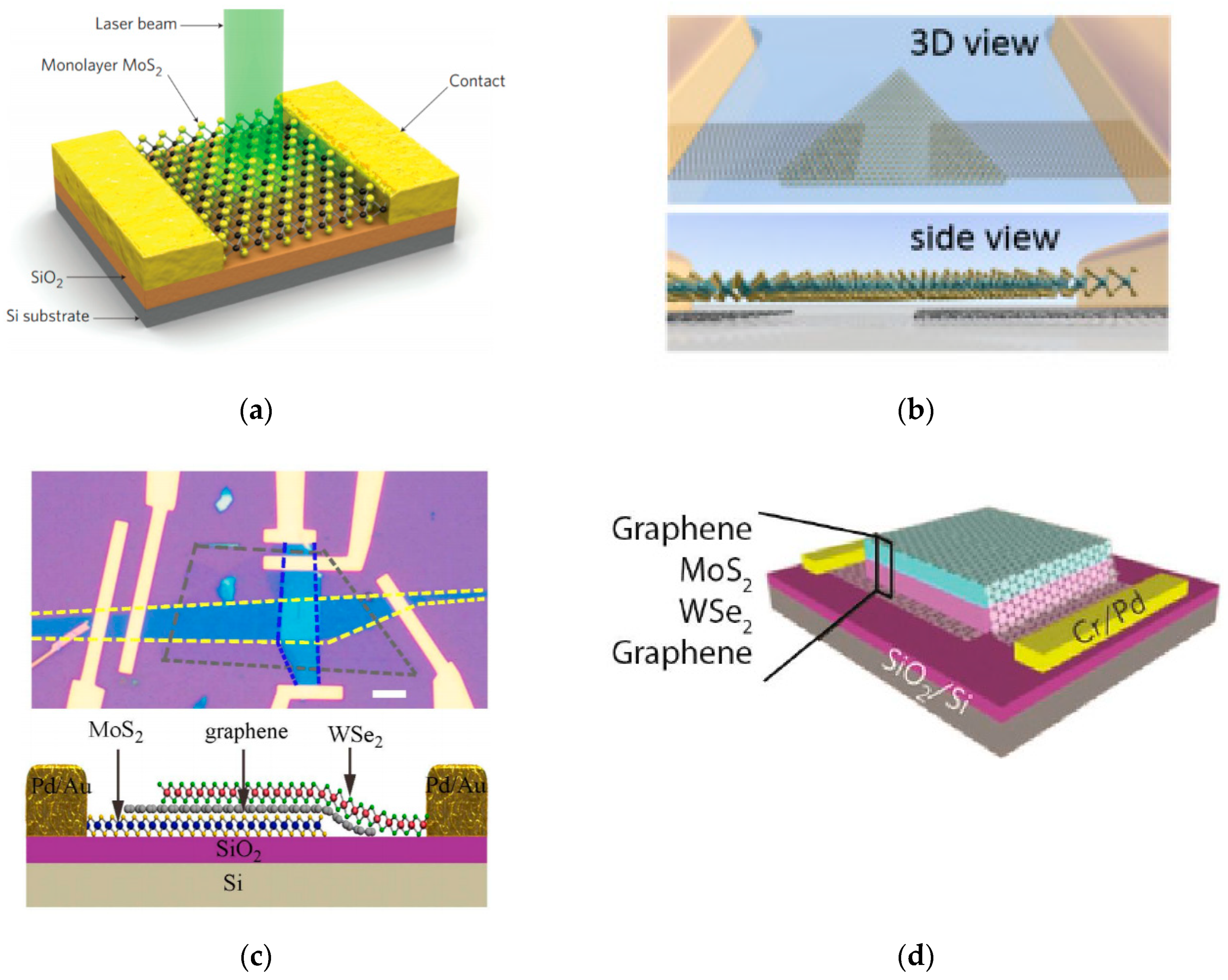
3.1. Mono- and Few-Layer Photodetectors
3.2. Heterostructure Photodetector Devices
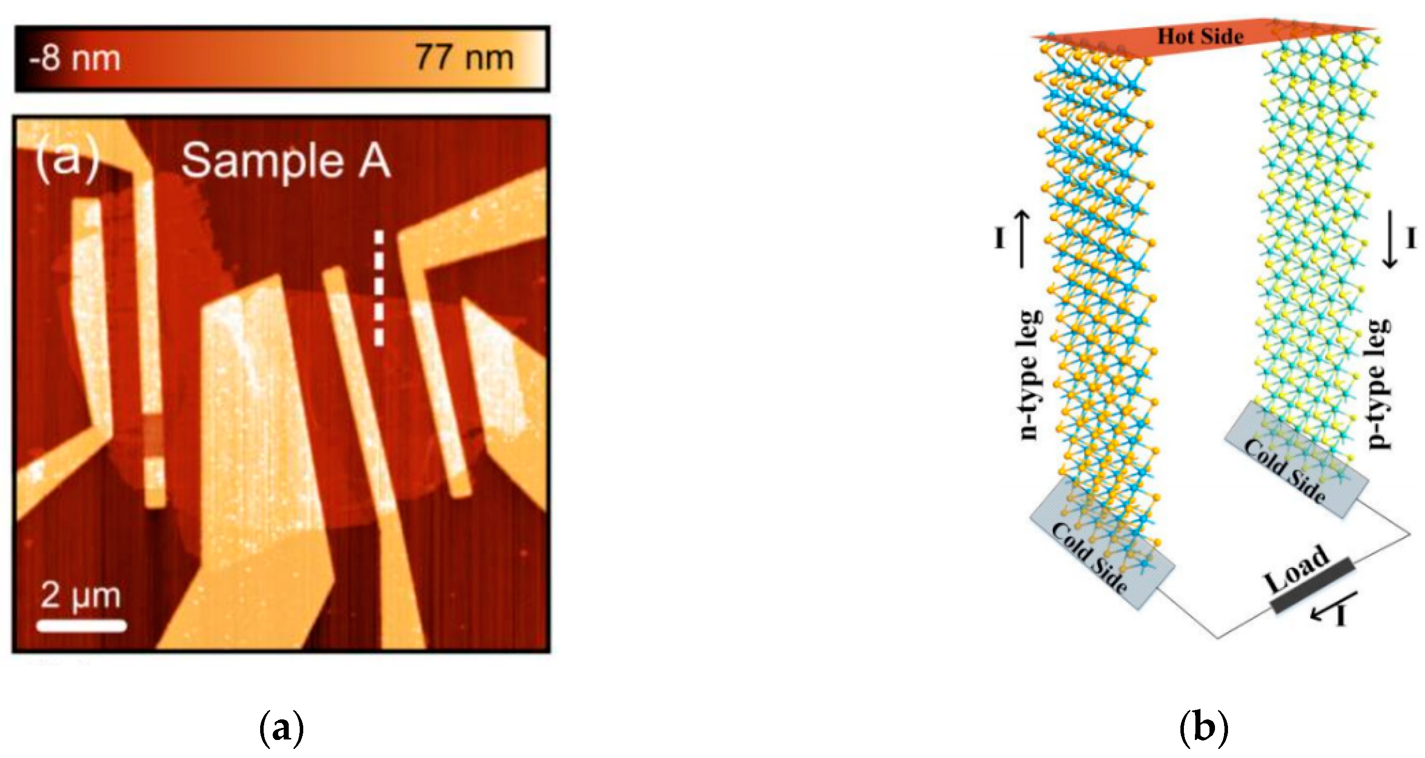
4. TMD-Based Thermocouple/Thermoelectric Devices
5. Challenges and Future Efforts
6. Conclusions
Author Contributions
Funding
Conflicts of Interest
References
- Novoselov, K.S.; Geim, A.K.; Morozov, S.V.; Jiang, D.; Zhang, Y.; Dubonos, S.V.; Grigorieva, I.V.; Firsov, A.A. Electric Field Effect in Atomically Thin Carbon Films. Science 2004, 306, 666–669. [Google Scholar] [CrossRef] [PubMed] [Green Version]
- Akinwande, D.; Brennan, C.J.; Bunch, J.S.; Egberts, P.; Felts, J.R.; Gao, H.; Huang, R.; Kim, J.S.; Li, T.; Li, Y.; et al. A review on mechanics and mechanical properties of 2D materials—Graphene and beyond. Extrem. Mech. Lett. 2017, 13, 42–77. [Google Scholar] [CrossRef] [Green Version]
- Bonaccorso, F.; Sun, Z.; Hasan, T.; Ferrari, A.C. Graphene photonics and optoelectronics. Nat. Photonics 2010, 4, 611–622. [Google Scholar] [CrossRef] [Green Version]
- Wang, Q.H.; Kalantar-Zadeh, K.; Kis, A.; Coleman, J.N.; Strano, M.S. Electronics and optoelectronics of two-dimensional transition metal dichalcogenides. Nat. Nanotechnol. 2012, 7, 699–712. [Google Scholar] [CrossRef]
- Pospischil, A.; Mueller, T. Optoelectronic Devices Based on Atomically Thin Transition Metal Dichalcogenides. Appl. Sci. 2016, 6, 78. [Google Scholar] [CrossRef] [Green Version]
- Choi, W.; Choudhary, N.; Han, G.H.; Park, J.; Akinwande, D.; Lee, Y.H. Recent development of two-dimensional transition metal dichalcogenides and their applications. Mater. Today 2017, 20, 116–130. [Google Scholar] [CrossRef]
- Han, S.A.; Sohn, A.; Kim, S.W. Recent advanced in energy harvesting and storage applications with two-dimensional layered materials. FlatChem 2017, 6, 37–47. [Google Scholar] [CrossRef]
- Gutiérrez, H.R.; Perea-López, N.; Elías, A.L.; Berkdemir, A.; Wang, B.; Lv, R.; López-Urías, F.; Crespi, V.H.; Terrones, H.; Terrones, M. Extraordinary Room-Temperature Photoluminescence in Triangular WS2 Monolayers. Nano Lett. 2013, 13, 3447–3454. [Google Scholar] [CrossRef] [Green Version]
- Mak, K.F.; Shan, J. Photonics and optoelectronics of 2D semiconductor transition metal dichalcogenides. Nat. Photonics 2016, 10, 216–226. [Google Scholar] [CrossRef]
- Wang, Q.; Lai, J.; Sun, D. Review of photo response in semiconductor transition metal dichalcogenides based photosensitive devices. Opt. Mater. Express 2016, 6, 2313–2327. [Google Scholar] [CrossRef]
- Lee, J.; Huang, J.; Sumpter, B.G.; Yoon, M. Strain-engineered optoelectronic properties of 2D transition metal dichalcogenide lateral heterostructures. 2D Mater. 2017, 4, 021016. [Google Scholar] [CrossRef]
- Lin, Z.; Carvalho, B.R.; Kahn, E.; Lv, R.; Rao, R.; Terrones, H.; Pimenta, M.A.; Terrones, M. Defect engineering of two-dimensional transition metal dichalcogenides. 2D Mater. 2016, 3, 022002. [Google Scholar] [CrossRef]
- Zhang, M.; Wu, J.; Zhu, Y.; Dumcenco, D.O.; Hong, J.; Mao, N.; Deng, S.; Chen, Y.; Yang, Y.; Jin, C.; et al. Two-Dimensional Molybdenum Tungsten Diselenide Alloys: Photoluminescence, Raman Scattering, and Electrical Transport. ACS Nano 2014, 8, 7130–7137. [Google Scholar] [CrossRef]
- Lee, Y.K.; Luo, Z.; Cho, S.P.; Kanatzidis, M.G.; Chung, I. Surface Oxide Removal for Polycrystalline SnSe Reveals Near-Single-Crystal Thermoelectric Performance. Joule 2019, 3, 719–731. [Google Scholar] [CrossRef] [Green Version]
- Christol, P.; Rodriguez, J.B. Progress on Type-II InAs/GaSb Superlattice (T2SL) Infrared Photodetector: From MWIR to VLWIR Spectral Domains. In Proceedings of the International Conference on Space Optics—ICSO 2014, 105632C, Tenerife, Spain, 7–10 October 2014; SPIE: Bellingham, WA, USA, 2014. [Google Scholar]
- Rogalski, A.; Martyniuk, P.; Kopytko, M. Challenges of small-pixel infrared detectors: A review. Rep. Prog. Phys. 2016, 79, 046501. [Google Scholar] [CrossRef]
- Arnob, M.M.P.; Nguyen, H.; Han, Z.; Shih, W.C. Compressed sensing hyperspectral imaging in the 0.9–2.5 um shortwave infrared wavelength range using a digital micromirror device and InGaAs linear array detector. Appl. Opt. 2018, 57, 5019–5024. [Google Scholar] [CrossRef]
- Huang, Z.; Zhang, T.; Liu, J.; Zhang, L.; Jin, Y.; Wang, J.; Jiang, K.; Fan, S.; Li, Q. Amorphous MoS2 Photodetector with Ultra-Broadband Response. ACS Appl. Electron. Mater. 2019, 1, 1314–1321. [Google Scholar] [CrossRef]
- Gu, X.; Yang, R. Phonon transport and thermal conductivity in two-dimensional materials. Annu. Rev. Heat Transf. 2016, 19. [Google Scholar] [CrossRef] [Green Version]
- Hippalgaonkar, K.; Wang, Y.; Ye, Y.; Qiu, D.Y.; Zhu, H.; Wang, Y.; Moore, J.; Louie, S.G.; Zhang, X. High thermoelectric power factor in two-dimensional crystals of MoS2. Phys. Rev. B 2017, 95, 115407. [Google Scholar] [CrossRef] [Green Version]
- Zhang, G.; Zhang, Y.W. Thermoelectric properties of two-dimensional transition metal dichalcogenides. J. Mater. Chem. C 2017, 5, 7684–7698. [Google Scholar] [CrossRef]
- Liu, Z.; Lau, S.P.; Yan, F. Functionalized graphene and other two-dimensional materials for photovoltaic devices: Device design and processing. Chem. Soc. Rev. 2015, 44, 5638–5679. [Google Scholar] [CrossRef]
- Planck, M. The Theory of Heat Radiation; Dover Publications: New York, NY, USA, 1991; pp. 221–245. ISBN 978-0-486-66811-8. [Google Scholar]
- Sze, S.M.; Ng, K.K. Physics of Semiconductor Devices; John Wiley & Sons: Hoboken, NJ, USA, 2006; ISBN 978-0-470-06830-4. [Google Scholar]
- Neamen, D. An Introduction to Semiconductor Devices, 1st ed.; McGraw-Hill, Inc.: New York, NY, USA, 2005; ISBN 978-0-07-298756-0. [Google Scholar]
- Sun, Y.; Thompson, S.E.; Nishida, T. Physics of strain effects in semiconductors and metal-oxide-semiconductor field-effect transistors. J. Appl. Phys. 2007, 101, 104503. [Google Scholar] [CrossRef]
- Yu, P.; Cardona, M. Fundamentals of Semiconductors: Physics and Materials Properties, 4th ed.; Graduate Texts in Physics; Springer: Berlin/Heidelberg, Germany, 2010; ISBN 978-3-642-00709-5. [Google Scholar]
- Ball, D.W. Wien’s Displacement Law as a Function of Frequency. J. Chem. Educ. 2013, 90, 1250–1252. [Google Scholar] [CrossRef]
- Hejazi, D.; Liu, S.; Ostadabbas, S.; Kar, S. Transition Metal Dichalcogenide Thin Films for Precise Optical Wavelength Estimation Using Bayesian Inference. ACS Appl. Nano Mater. 2019, 2, 4075–4084. [Google Scholar] [CrossRef]
- Goldsmid, J. The Physics of Thermoelectric Energy Conversion; Morgan & Claypool Publishers: San Rafael, CA, USA, 2017; ISBN 978-1-68174-641-8. [Google Scholar]
- Bahk, J.H.; Shakouri, A. Minority carrier blocking to enhance the thermoelectric figure of merit in narrow-band-gap semiconductors. Phys. Rev. B 2016, 93, 165209. [Google Scholar] [CrossRef]
- Zhao, L.D.; Lo, S.H.; Zhang, Y.; Sun, H.; Tan, G.; Uher, C.; Wolverton, C.; Dravid, V.P.; Kanatzidis, M.G. Ultralow thermal conductivity and high thermoelectric figure of merit in SnSe crystals. Nature 2014, 508, 373–377. [Google Scholar] [CrossRef] [PubMed]
- Hinterleitner, B.; Knapp, I.; Poneder, M.; Shi, Y.; Müller, H.; Eguchi, G.; Eisenmenger-Sittner, C.; Stöger-Pollach, M.; Kakefuda, Y.; Kawamoto, N.; et al. Thermoelectric performance of a metastable thin-film Heusler alloy. Nature 2019, 576, 85–90. [Google Scholar] [CrossRef] [PubMed]
- Kang, J.; Zhang, L.; Wei, S.H. A Unified Understanding of the Thickness-Dependent Bandgap Transition in Hexagonal Two-Dimensional Semiconductors. J. Phys. Chem. Lett. 2016, 7, 597–602. [Google Scholar] [CrossRef]
- Liu, H.L.; Shen, C.C.; Su, S.H.; Hsu, C.L.; Li, M.Y.; Li, L.J. Optical properties of monolayer transition metal dichalcogenides probed by spectroscopic ellipsometry. Appl. Phys. Lett. 2014, 105, 201905. [Google Scholar] [CrossRef] [Green Version]
- Kumar, A.; Ahluwalia, P.K. Electronic structure of transition metal dichalcogenides monolayers 1H-MX2 (M = Mo, W; X = S, Se, Te) from ab-initio theory: New direct band gap semiconductors. Eur. Phys. J. B 2012, 85, 186. [Google Scholar] [CrossRef]
- Lopez-Sanchez, O.; Lembke, D.; Kayci, M.; Radenovic, A.; Kis, A. Ultrasensitive photodetectors based on monolayer MoS2. Nat. Nanotechnol. 2013, 8, 497–501. [Google Scholar] [CrossRef] [PubMed]
- Yu, Z.; Pan, Y.; Shen, Y.; Wang, Z.; Ong, Z.Y.; Xu, T.; Xin, R.; Pan, L.; Wang, B.; Sun, L.; et al. Towards intrinsic charge transport in monolayer molybdenum disulfide by defect and interface engineering. Nat. Commun. 2014, 5, 5290. [Google Scholar] [CrossRef]
- Zhang, W.; Huang, Z.; Zhang, W.; Li, Y. Two-dimensional semiconductors with possible high room temperature mobility. Nano Res. 2014, 7, 1731–1737. [Google Scholar] [CrossRef] [Green Version]
- Ge, Y.; Wan, W.; Feng, W.; Xiao, D.; Yao, Y. Effect of doping and strain modulations on electron transport in monolayer MoS2. Phys. Rev. B 2014, 90, 035414. [Google Scholar] [CrossRef] [Green Version]
- Phuc, H.V.; Hieu, N.N.; Hoi, B.D.; Hieu, N.V.; Thu, T.V.; Hung, N.M.; Ilyasov, V.V.; Poklonski, N.A.; Nguyen, C.V. Tuning the Electronic Properties, Effective Mass and Carrier Mobility of MoS2 Monolayer by Strain Engineering: First-Principle Calculations. J. Electron. Mater. 2018, 47, 730–736. [Google Scholar] [CrossRef]
- Koperski, M.; Molas, M.R.; Arora, A.; Nogajewski, K.; Slobodeniuk, A.O.; Faugeras, C.; Potemski, M. Optical properties of atomically thin transition metal dichalcogenides: Observations and puzzles. Nanophotonics 2017, 6, 1289–1308. [Google Scholar] [CrossRef]
- Frisenda, R.; Niu, Y.; Gant, P.; Molina-Mendoza, A.J.; Schmidt, R.; Bratschitsch, R.; Liu, J.; Fu, L.; Dumcenco, D.; Kis, A.; et al. Micro-reflectance and transmittance spectroscopy: A versatile and powerful tool to characterize 2D materials. J. Phys. Appl. Phys. 2017, 50, 074002. [Google Scholar] [CrossRef]
- Zhang, C.; Wang, H.; Chan, W.; Manolatou, C.; Rana, F. Absorption of light by excitons and trions in monolayers of metal dichalcogenide MoS2: Experiments and theory. Phys. Rev. B 2014, 89, 205436. [Google Scholar] [CrossRef] [Green Version]
- Butun, S.; Palacios, E.; Cain, J.D.; Liu, Z.; Dravid, V.P.; Aydin, K. Quantifying Plasmon-Enhanced Light Absorption in Monolayer WS2 Films. ACS Appl. Mater. Interfaces 2017, 9, 15044–15051. [Google Scholar] [CrossRef]
- Huo, D.; Zhang, J.; Wang, H.; Ren, X.; Wang, C.; Su, H.; Zhao, H. Broadband Perfect Absorber with Monolayer MoS2 and Hexagonal Titanium Nitride Nano-disk Array. Nanoscale Res. Lett. 2017, 12, 465. [Google Scholar] [CrossRef] [Green Version]
- Lee, H.S.; Min, S.W.; Chang, Y.G.; Park, M.K.; Nam, T.; Kim, H.; Kim, J.H.; Ryu, S.; Im, S. MoS2 Nanosheet Phototransistors with Thickness-Modulated Optical Energy Gap. Nano Lett. 2012, 12, 3695–3700. [Google Scholar] [CrossRef] [PubMed]
- Park, M.J.; Park, K.; Ko, H. Near-infrared photodetector achieved by chemically-exfoliated multilayered MoS2 flakes. Appl. Surf. Sci. 2018, 448, 64–70. [Google Scholar] [CrossRef]
- Rai, D.P.; Vu, T.V.; Laref, A.; Ghimire, M.P.; Patra, P.K.; Srivastava, S. Electronic and optical properties of 2D monolayer (ML) MoS2 with vacancy defect at S sites. Nano-Struct. Nano-Objects 2020, 21, 100404. [Google Scholar] [CrossRef]
- Huang, H.; Wang, J.; Hu, W.; Liao, L.; Wang, P.; Wang, X.; Gong, F.; Chen, Y.; Wu, G.; Luo, W.; et al. Highly sensitive visible to infrared MoTe2 photodetectors enhanced by the photogating effect. Nanotechnology 2016, 27, 445201. [Google Scholar] [CrossRef] [PubMed]
- Buscema, M.; Island, J.O.; Groenendijk, D.J.; Blanter, S.I.; Steele, G.A.; van der Zant, H.S.J.; Castellanos-Gomez, A. Photocurrent generation with two-dimensional van der Waals semiconductors. Chem. Soc. Rev. 2015, 44, 3691–3718. [Google Scholar] [CrossRef] [Green Version]
- Griffin, M.K.; Burke, H.K.; Kerekes, J.P. Understanding radiative transfer in the midwave infrared: A precursor to full-spectrum atmospheric compensation. In Proceedings of the Algorithms and Technologies for Multispectral, Hyperspectral, and Ultraspectral Imagery X, Orlando, FL, USA, 12–15 April 2004; Shen, S.S., Lewis, P.E., Eds.; SPIE: Bellingham, WA, USA, 2004; Volume 5425, pp. 348–356. [Google Scholar]
- Xie, Y.; Liang, F.; Wang, D.; Chi, S.; Yu, H.; Lin, Z.; Zhang, H.; Chen, Y.; Wang, J.; Wu, Y. Room-Temperature Ultrabroadband Photodetection with MoS2 by Electronic-Structure Engineering Strategy. Adv. Mater. 2018, 30, 1804858. [Google Scholar] [CrossRef]
- Tan, H.; Fan, Y.; Zhou, Y.; Chen, Q.; Xu, W.; Warner, J.H. Ultrathin 2D Photodetectors Utilizing Chemical Vapor Deposition Grown WS2 With Graphene Electrodes. ACS Nano 2016, 10, 7866–7873. [Google Scholar] [CrossRef]
- Britnell, L.; Ribeiro, R.M.; Eckmann, A.; Jalil, R.; Belle, B.D.; Mishchenko, A.; Kim, Y.J.; Gorbachev, R.V.; Georgiou, T.; Morozov, S.V.; et al. Strong Light-Matter Interactions in Heterostructures of Atomically Thin Films. Science 2013, 340, 1311–1314. [Google Scholar] [CrossRef] [Green Version]
- Tsai, D.S.; Liu, K.K.; Lien, D.H.; Tsai, M.L.; Kang, C.F.; Lin, C.A.; Li, L.J.; He, J.H. Few-Layer MoS2 with High Broadband Photogain and Fast Optical Switching for Use in Harsh Environments. ACS Nano 2013, 7, 3905–3911. [Google Scholar] [CrossRef]
- Long, M.; Liu, E.; Wang, P.; Gao, A.; Xia, H.; Luo, W.; Wang, B.; Zeng, J.; Fu, Y.; Xu, K.; et al. Broadband Photovoltaic Detectors Based on an Atomically Thin Heterostructure. Nano Lett. 2016, 16, 2254–2259. [Google Scholar] [CrossRef]
- Kim, D.; Lee, R.; Kim, S.; Kim, T. Two-dimensional phase-engineered 1T′– and 2H–MoTe2-based near-infrared photodetectors with ultra-fast response. J. Alloys Compd. 2019, 789, 960–965. [Google Scholar] [CrossRef]
- Dhyani, V.; Das, S. High-Speed Scalable Silicon-MoS2 P-N Heterojunction Photodetectors. Sci. Rep. 2017, 7, 44243. [Google Scholar] [CrossRef]
- Wu, E.; Wu, D.; Jia, C.; Wang, Y.; Yuan, H.; Zeng, L.; Xu, T.; Shi, Z.; Tian, Y.; Li, X. In Situ Fabrication of 2D WS2/Si Type-II Heterojunction for Self-Powered Broadband Photodetector with Response up to Mid-Infrared. ACS Photonics 2019, 6, 565–572. [Google Scholar] [CrossRef] [Green Version]
- Pataniya, P.M.; Sumesh, C.K. Low cost and flexible photodetector based on WSe2 Nanosheets/Graphite heterostructure. Synth. Met. 2020, 265, 116400. [Google Scholar] [CrossRef]
- Zhang, K.; Peng, M.; Wu, W.; Guo, J.; Gao, G.; Liu, Y.; Kou, J.; Wen, R.; Lei, Y.; Yu, A.; et al. A flexible p-CuO/n-MoS2 heterojunction photodetector with enhanced photoresponse by the piezo-phototronic effect. Mater. Horiz. 2017, 4, 274–280. [Google Scholar] [CrossRef]
- Xue, Y.; Zhang, Y.; Liu, Y.; Liu, H.; Song, J.; Sophia, J.; Liu, J.; Xu, Z.; Xu, Q.; Wang, Z.; et al. Scalable Production of a Few-Layer MoS2/WS2 Vertical Heterojunction Array and Its Application for Photodetectors. ACS Nano 2016, 10, 573–580. [Google Scholar] [CrossRef] [PubMed]
- Lee, C.H.; Lee, G.H.; van der Zande, A.M.; Chen, W.; Li, Y.; Han, M.; Cui, X.; Arefe, G.; Nuckolls, C.; Heinz, T.F.; et al. Atomically thin p–n junctions with van der Waals heterointerfaces. Nat. Nanotechnol. 2014, 9, 676–681. [Google Scholar] [CrossRef] [Green Version]
- Velusamy, D.B.; Kim, R.H.; Cha, S.; Huh, J.; Khazaeinezhad, R.; Kassani, S.H.; Song, G.; Cho, S.M.; Cho, S.H.; Hwang, I.; et al. Flexible transition metal dichalcogenide nanosheets for band-selective photodetection. Nat. Commun. 2015, 6, 8063. [Google Scholar] [CrossRef] [Green Version]
- Gao, L. Flexible Device Applications of 2D Semiconductors. Small 2017, 13, 1603994. [Google Scholar] [CrossRef] [PubMed]
- Li, J.; Han, J.; Li, H.; Fan, X.; Huang, K. Large-area, flexible broadband photodetector based on WS2 nanosheets films. Mater. Sci. Semicond. Process. 2020, 107, 104804. [Google Scholar] [CrossRef]
- Gomathi, P.T.; Sahatiya, P.; Badhulika, S. Large-Area, Flexible Broadband Photodetector Based on ZnS–MoS2 Hybrid on Paper Substrate. Adv. Funct. Mater. 2017, 27, 1701611. [Google Scholar] [CrossRef]
- Peng, Y.; Que, M.; Tao, J.; Wang, X.; Lu, J.; Hu, G.; Wan, B.; Xu, Q.; Pan, C. Progress in piezotronic and piezo-phototronic effect of 2D materials. 2D Mater. 2018, 5, 042003. [Google Scholar] [CrossRef] [Green Version]
- Chung, D.Y.; Hogan, T.P.; Rocci-Lane, M.; Brazis, P.; Ireland, J.R.; Kannewurf, C.R.; Bastea, M.; Uher, C.; Kanatzidis, M.G. A New Thermoelectric Material: CsBi4Te6. J. Am. Chem. Soc. 2004, 126, 6414–6428. [Google Scholar] [CrossRef]
- Wickramaratne, D.; Zahid, F.; Lake, R.K. Electronic and thermoelectric properties of few-layer transition metal dichalcogenides. J. Chem. Phys. 2014, 140, 124710. [Google Scholar] [CrossRef] [Green Version]
- Amollo, T.A.; Mola, G.T.; Kirui, M.S.K.; Nyamori, V.O. Graphene for Thermoelectric Applications: Prospects and Challenges. Crit. Rev. Solid State Mater. Sci. 2018, 43, 133–157. [Google Scholar] [CrossRef]
- Balandin, A.A.; Ghosh, S.; Bao, W.; Calizo, I.; Teweldebrhan, D.; Miao, F.; Lau, C.N. Superior Thermal Conductivity of Single-Layer Graphene. Nano Lett. 2008, 8, 902–907. [Google Scholar] [CrossRef]
- Sahoo, S.; Gaur, A.P.S.; Ahmadi, M.; Guinel, M.J.F.; Katiyar, R.S. Temperature-Dependent Raman Studies and Thermal Conductivity of Few-Layer MoS2. J. Phys. Chem. C 2013, 117, 9042–9047. [Google Scholar] [CrossRef] [Green Version]
- Cai, Y.; Lan, J.; Zhang, G.; Zhang, Y.W. Lattice vibrational modes and phonon thermal conductivity of monolayer MoS2. Phys. Rev. B 2014, 89, 035438. [Google Scholar] [CrossRef] [Green Version]
- Zhang, G.; Zhang, Y.W. Strain effects on thermoelectric properties of two-dimensional materials. Mech. Mater. 2015, 91, 382–398. [Google Scholar] [CrossRef]
- Williamson, I.; Li, S.; Correa Hernandez, A.; Lawson, M.; Chen, Y.; Li, L. Structural, electrical, phonon, and optical properties of Ti- and V-doped two-dimensional MoS2. Chem. Phys. Lett. 2017, 674, 157–163. [Google Scholar] [CrossRef]
- Kayyalha, M.; Maassen, J.; Lundstrom, M.; Shi, L.; Chen, Y.P. Gate-tunable and thickness-dependent electronic and thermoelectric transport in few-layer MoS2. J. Appl. Phys. 2016, 120, 134305. [Google Scholar] [CrossRef] [Green Version]
- Liu, X.; Zhang, Y.W. Thermal properties of transition-metal dichalcogenide. Chin. Phys. B 2018, 27, 034402. [Google Scholar] [CrossRef]
- Rull-Bravo, M.; Moure, A.; Fernández, J.F.; Martín-González, M. Skutterudites as thermoelectric materials: Revisited. RSC Adv. 2015, 5, 41653–41667. [Google Scholar] [CrossRef]
- Huang, W.; Da, H.; Liang, G. Thermoelectric performance of MX2 (M = Mo,W; X = S,Se) monolayers. J. Appl. Phys. 2013, 113, 104304. [Google Scholar] [CrossRef]
- Peng, B.; Zhang, H.; Shao, H.; Xu, Y.; Zhang, X.; Zhu, H. Thermal conductivity of monolayer MoS2, MoSe2, and WS2: Interplay of mass effect, interatomic bonding and anharmonicity. RSC Adv. 2016, 6, 5767–5773. [Google Scholar] [CrossRef] [Green Version]
- Ge, Y.; Wan, W.; Ren, Y.; Liu, Y. Large thermoelectric power factor of high-mobility transition-metal dichalcogenides with 1T” phase. Phys. Rev. Res. 2020, 2, 013134. [Google Scholar] [CrossRef] [Green Version]
- Babaei, H.; Khodadadi, J.M.; Sinha, S. Large theoretical thermoelectric power factor of suspended single-layer MoS2. Appl. Phys. Lett. 2014, 105, 193901. [Google Scholar] [CrossRef]
- Buscema, M.; Barkelid, M.; Zwiller, V.; van der Zant, H.S.J.; Steele, G.A.; Castellanos-Gomez, A. Large and Tunable Photothermoelectric Effect in Single-Layer MoS2. Nano Lett. 2013, 13, 358–363. [Google Scholar] [CrossRef] [Green Version]
- Yoshida, M.; Iizuka, T.; Saito, Y.; Onga, M.; Suzuki, R.; Zhang, Y.; Iwasa, Y.; Shimizu, S. Gate-Optimized Thermoelectric Power Factor in Ultrathin WSe2 Single Crystals. Nano Lett. 2016, 16, 2061–2065. [Google Scholar] [CrossRef]
- Pu, J.; Kanahashi, K.; Cuong, N.T.; Chen, C.H.; Li, L.J.; Okada, S.; Ohta, H.; Takenobu, T. Enhanced thermoelectric power in two-dimensional transition metal dichalcogenide monolayers. Phys. Rev. B 2016, 94, 014312. [Google Scholar] [CrossRef] [Green Version]
- Yarali, M.; Wu, X.; Gupta, T.; Ghoshal, D.; Xie, L.; Zhu, Z.; Brahmi, H.; Bao, J.; Chen, S.; Luo, T.; et al. Effects of Defects on the Temperature-Dependent Thermal Conductivity of Suspended Monolayer Molybdenum Disulfide Grown by Chemical Vapor Deposition. Adv. Funct. Mater. 2017, 27, 1704357. [Google Scholar] [CrossRef]
- Chen, D.; Chen, H.; Hu, S.; Guo, H.; Sharshir, S.W.; An, M.; Ma, W.; Zhang, X. Influence of atomic-scale defect on thermal conductivity of single-layer MoS2 sheet. J. Alloys Compd. 2020, 831, 154875. [Google Scholar] [CrossRef]
- Alexandre Adessi, C.; Pecorario, S.; Thebaud, S.; Bouzerar, G. First Principle Investigation of the Influence of Sulfur Vacancies on the Thermoelectric Properties of Single Layered MoS2. Phys. Chem. Chem. Phys. 2020. [Google Scholar] [CrossRef]
- Zhang, Y.; Stucky, G.D. Heterostructured Approaches to Efficient Thermoelectric Materials. Chem. Mater. 2014, 26, 837–848. [Google Scholar] [CrossRef]
- Wang, T.; Liu, C.; Jiang, F.; Xu, Z.; Wang, X.; Li, X.; Li, C.; Xu, J.; Yang, X. Solution-processed two-dimensional layered heterostructure thin-film with optimized thermoelectric performance. Phys. Chem. Chem. Phys. 2017, 19, 17560–17567. [Google Scholar] [CrossRef]
- Oh, J.; Kim, Y.; Chung, S.; Kim, H.; Son, J.G. Fabrication of a MoS2/Graphene Nanoribbon Heterojunction Network for Improved Thermoelectric Properties. Adv. Mater. Interfaces 2019, 6, 1901333. [Google Scholar] [CrossRef]
- Oh, J.; Yoo, H.; Choi, J.; Kim, J.Y.; Lee, D.S.; Kim, M.J.; Lee, J.C.; Kim, W.N.; Grossman, J.C.; Park, J.H.; et al. Significantly reduced thermal conductivity and enhanced thermoelectric properties of single- and bi-layer graphene nanomeshes with sub-10nm neck-width. Nano Energy 2017, 35, 26–35. [Google Scholar] [CrossRef]
- Wang, T.; Liu, C.; Wang, X.; Li, X.; Jiang, F.; Li, C.; Hou, J.; Xu, J. Highly enhanced thermoelectric performance of WS2 nanosheets upon embedding PEDOT:PSS. J. Polym. Sci. Part B Polym. Phys. 2017, 55, 997–1004. [Google Scholar] [CrossRef]
- Li, X.; Liu, C.; Wang, T.; Wang, W.; Wang, X.; Jiang, Q.; Jiang, F.; Xu, J. Preparation of 2D MoSe2/PEDOT:PSS composite and its thermoelectric properties. Mater. Res. Express 2017, 4, 116410. [Google Scholar] [CrossRef]
- Wu, T.; Xu, R.; Zheng, X.; Zhuang, W. Electronic Structures and Thermoelectric Properties of Two-Dimensional MoS2/MoSe2 Heterostructures. Chin. J. Chem. Phys. 2016, 29, 445–452. [Google Scholar] [CrossRef]
- Arab, A.; Li, Q. Anisotropic thermoelectric behavior in armchair and zigzag mono- and fewlayer MoS2 in thermoelectric generator applications. Sci. Rep. 2015, 5, 13706. [Google Scholar] [CrossRef] [Green Version]
- Lee, C.; Hong, J.; Whangbo, M.H.; Shim, J.H. Enhancing the Thermoelectric Properties of Layered Transition-Metal Dichalcogenides 2H-MQ2 (M = Mo, W; Q = S, Se, Te) by Layer Mixing: Density Functional Investigation. Chem. Mater. 2013, 25, 3745–3752. [Google Scholar] [CrossRef]
- Ouyang, Y.; Xie, Y.; Zhang, Z.; Peng, Q.; Chen, Y. Very high thermoelectric figure of merit found in hybrid transition-metal-dichalcogenides. J. Appl. Phys. 2016, 120, 235109. [Google Scholar] [CrossRef] [Green Version]
- Sledzinska, M.; Graczykowski, B.; Placidi, M.; Reig, D.S.; Sachat, A.E.; Reparaz, J.S.; Alzina, F.; Roche, S.; Mortazavi, B.; Quey, R.; et al. Thermal conductivity of MoS2 polycrystalline nanosheets. arXiv 2016, arXiv:160404865. [Google Scholar]
- Wang, S.; Pacios, M.; Bhaskaran, H.; Warner, J.H. Substrate control for large area continuous films of monolayer MoS2 by atmospheric pressure chemical vapor deposition. Nanotechnology 2016, 27, 085604. [Google Scholar] [CrossRef]
- Amani, M.; Chin, M.L.; Mazzoni, A.L.; Burke, R.A.; Najmaei, S.; Ajayan, P.M.; Lou, J.; Dubey, M. Growth-substrate induced performance degradation in chemically synthesized monolayer MoS2 field effect transistors. Appl. Phys. Lett. 2014, 104, 203506. [Google Scholar] [CrossRef] [Green Version]
- Ahn, S.; Kim, G.; Nayak, P.K.; Yoon, S.I.; Lim, H.; Shin, H.J.; Shin, H.S. Prevention of Transition Metal Dichalcogenide Photodegradation by Encapsulation with h-BN Layers. ACS Nano 2016, 10, 8973–8979. [Google Scholar] [CrossRef]
- Şar, H.; Özden, A.; Demiroğlu, İ.; Sevik, C.; Perkgoz, N.K.; Ay, F. Long-Term Stability Control of CVD-Grown Monolayer MoS2. Phys. Status Solidi RRL Rapid Res. Lett. 2019, 13, 1800687. [Google Scholar] [CrossRef]
- Kufer, D.; Nikitskiy, I.; Lasanta, T.; Navickaite, G.; Koppens, F.H.L.; Konstantatos, G. Hybrid 2D-0D MoS2 -PbS quantum dot photodetectors. Adv. Mater. Deerfield Beach Fla 2015, 27, 176–180. [Google Scholar] [CrossRef]
- Popov, I.; Seifert, G.; Tománek, D. Designing Electrical Contacts to MoS2 Monolayers: A Computational Study. Phys. Rev. Lett. 2012, 108, 156802. [Google Scholar] [CrossRef] [PubMed] [Green Version]
- Liu, D.; Guo, Y.; Fang, L.; Robertson, J. Sulfur vacancies in monolayer MoS2 and its electrical contacts. Appl. Phys. Lett. 2013, 103, 183113. [Google Scholar] [CrossRef]
- Brown, D.B.; Shen, W.; Li, X.; Xiao, K.; Geohegan, D.B.; Kumar, S. Spatial Mapping of Thermal Boundary Conductance at Metal–Molybdenum Diselenide Interfaces. ACS Appl. Mater. Interfaces 2019, 11, 14418–14426. [Google Scholar] [CrossRef] [PubMed]


| Temperature | Photon Energy Peak (eV) | Peak Wavelength (nm) | Application/Reference |
|---|---|---|---|
| 290 K | 0.124 | 9992 | Common outside temperature 70 deg F |
| 310 K | 0.132 | 9348 | Human body temperature (98 deg F) |
| 373 K | 0.16 | 7769 | Water boiling temperature |
| 1300 K | 0.56 | 2229 | Flowing lava, open flame |
| 3500 K | 1.49 | 828 | Rocket combustion temperature |
| 5800 K | 2.47 | 500 nm | Surface temperature of the Sun |
| Material | Layers | Spectral Range (nm) | Responsivity | Detectivity | Response Time (Rise/Fall) | Reference |
|---|---|---|---|---|---|---|
| MoS2 | 1 | 400–680 | 880 | - | - | [37] |
| MoS2 | 3 | 380–800 | 0.57 | 1010 | 70/110 µs | [56] |
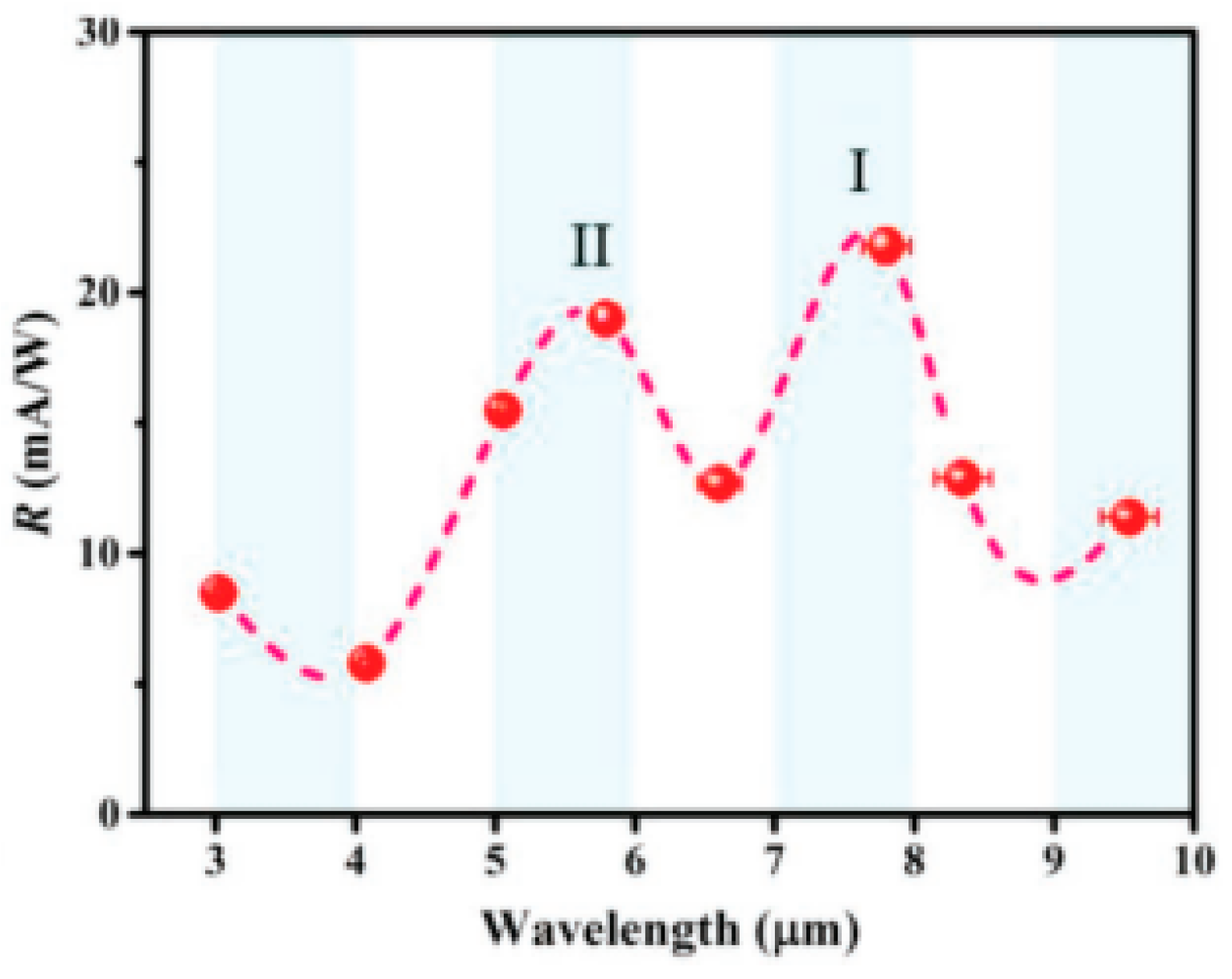
| MoS2 | >40 | 445–9500 | 21.8 (At 7790 nm) | - | - | [53] |
| AgNPs-MoS2 | ~8–40 | 400–1600 | 0.881 mA/W | 1.28 × 10⁹ J | [48] | |
| MoS22/1L-Gr/WSe2 | 3 | 400–2400 | Visible–104 A/W 2400 nm–~1A/W | Visible- 1015 Jones 2400 nm- 109 Jones | 30 ms (rise) | [57] |
| MoTe2 (mechanically exfoliated) | 2H? | 600–1750 | 24 mA/W | 1.3 × 10⁹ | - | [50] |
| 1T’ MoTe2 | 4 | 500–1100 | 62–109 mA/W | - | 0.82 µs (rise) 7.29 (fall) | [58] |
| Si/MoS2 heterojunction | 6–10 | 450–1000 | 8.75 A/W | 1.28 × 10⁹ J | 10/19 s | [59] |
| WS2/Si (Type II) | ~5 | 200–3043 | 224 mA/W | 1.5 × 10¹² J | 16/29 µs | [60] |
| WS2/graphite on paper | Nanosheets | 390–1080 | 6.66 mA/W | 1.94 × 10⁸ J | 800/1400 ms | [61] |
| p-CuO/n-MoS2 | 1 | - | 11.4 mA/W | 3.27 × 10⁸ J | - | [62] |
| Material/Type | Layers | (S/cm) | (Wm−1K−1) | ZT | Temperature | Reference | ||
|---|---|---|---|---|---|---|---|---|
| p-MoS2 (theoretical) | 1 | - | - | - | 0.55 | 300 K | [81] | |
| n-WSe2 (theoretical) | 1 | - | - | - | 1.1 | 500 K | [81] | |
| MoS2 | 1 | - | −4 × 10² −1 × 10⁵ | - | - | - | [85] | |
| n-WSe2 and p-MoS2 | 1 | >200 | >200 | 1.5 (from [101]) | 0.1 | 300 K | [87] | |
| WSe2 (gate optimized) | 3 | 3200 (n-type) 3700 (p-type) | ~100 | ~5 × 10³ | - | - | 300 K | [86] |
| rGO-MoS2 | - | 15.1 | ~80 | 130.8 | 0.206 | 0.022 | 300 K | [92] |
| rGO-WS2 | - | 17.4 | ~80 | 136.4 | 0.208 | 0.025 | 300 K | [92] |
| WS2 PEDOT:PSS (50%) | Nano-sheets | 45.2 | ~83 | 1333 | 0.36 (cross-plane) 1.2 (in-plane) | 0.01 | 300 K | [95] |
| MoS2/MoSe2 (armchair) | Nano-ribbon | - | ~600 | - | - | 7.4 | 800 K | [100] |
© 2020 by the authors. Licensee MDPI, Basel, Switzerland. This article is an open access article distributed under the terms and conditions of the Creative Commons Attribution (CC BY) license (http://creativecommons.org/licenses/by/4.0/).
Share and Cite
Voshell, A.; Terrones, M.; Rana, M. Thermal and Photo Sensing Capabilities of Mono- and Few-Layer Thick Transition Metal Dichalcogenides. Micromachines 2020, 11, 693. https://doi.org/10.3390/mi11070693
Voshell A, Terrones M, Rana M. Thermal and Photo Sensing Capabilities of Mono- and Few-Layer Thick Transition Metal Dichalcogenides. Micromachines. 2020; 11(7):693. https://doi.org/10.3390/mi11070693
Chicago/Turabian StyleVoshell, Andrew, Mauricio Terrones, and Mukti Rana. 2020. "Thermal and Photo Sensing Capabilities of Mono- and Few-Layer Thick Transition Metal Dichalcogenides" Micromachines 11, no. 7: 693. https://doi.org/10.3390/mi11070693