Article

Characterization and Analysis of Metal Adhesion to Parylene Polymer Substrate Using Scotch Tape Test for Peripheral Neural Probe

1
Center for Nanoscience and Nanotechnology (C2N), University-Paris-Saclay, Orsay 91400, France
2
Center for Bionics, Korea Institute of Science and Technology (KIST), Seongbuk-gu, Seoul 02792, Korea
*
Author to whom correspondence should be addressed.
Both authors are equally-contributed to this manuscript.
Micromachines 2020, 11(6), 605; https://doi.org/10.3390/mi11060605
Submission received: 3 June 2020 / Revised: 18 June 2020 / Accepted: 19 June 2020 / Published: 22 June 2020
(This article belongs to the Special Issue MEMS Packaging Technologies and 3D Integration)

Abstract

:
This paper presents measurement and FEM (Finite Element Method) analysis of metal adhesion force to a parylene substrate for implantable neural probe. A test device composed of 300 nm-thick gold and 30 nm-thick titanium metal electrodes on top of parylene substrate was prepared. The metal electrodes suffer from delamination during wet metal patterning process; thus, CF4 plasma treatment was applied to the parylene substrate before metal deposition. The two thin film metal layers were deposited by e-beam evaporation process. Metal electrodes had 200 μm in width, 300 μm spacing between the metal lines, and 5 mm length as the neural probe. Adhesion force of the metal lines to parylene substrate was measured with scotch tape test. Angle between the scotch tape and the test device substrate changed from 60° to 90° during characterization. Force exerted the scotch tape was recorded as the function of displacement of the scotch tape. It was found that a peak was created in measured force-displacement curve due to metal delamination. Metal adhesion was estimated 1.3 J/m2 by referring to the force peak and metal width at the force-displacement curve. Besides, the scotch tape test was simulated to comprehend delamination behavior of the test through FEM modeling.

1. Introduction

Many research efforts have been made to develop and improve of the prosthetic hands and arms for the amputees, and, in recent years, much progress has been observed in the development of life-like robotic hands and the means of controlling them with greater degree of freedom. For this purpose, micro-electro-mechanical systems (MEMS) technologies have been used to fabricate neural interface probes [1,2,3,4,5,6]. However, existing MEMS-based neural electrodes would have a limitation on the neural interface due to its material characteristics. Thus, flexible neural electrodes have been recently proposed to minimize mechanical mismatch between the electrode and tissue after the electrode’s implantation for a stable long-term recording and stimulation. To this sense, peripheral neural interface (PNI) devices have appeared to retrieve and send neural signals directly from and to the residual or existing peripheral nerves in this field [7]. Recently, thin film flexible polymeric devices are being used for measuring nerve impulse from the central or peripheral nerve systems [8,9,10,11,12,13]. Such flexible polymeric devices tend to be designed several μm in thickness and a few mm in length due to its nature of interfacing with neurons in human body. Consequently, metal electrodes on such a thin and long polymeric substrate have constraints to be at best several hundred nanometers. Thus, metallization technology frequently used is PVD (Physical Vapor Deposition), such as evaporation or sputtering. The PVD metal layers are formed into long and thin metal lines through wet-etch or lift-off technique. Although thin-film polymeric devices are flexible and biocompatible, they are prone to delamination and carry concerns about their mechanical robustness [14]. A nanopillar array created by plasma etching could be used to enhance adhesion among different materials in the parylene-metal-parylene system [15]. ALD (Atomic layer deposition) Al2O3 combined with the silane adhesion promoter A-174 would increase adhesion force between two parylene films [14]. Parylene material has been shown that mechanical properties can be maintained after stored in PBS (Phosphate Buffered Saline) solution up to 12 months [16]. Therefore, mechanical or chemical treatments of the interface between polymer substrate and metal film is frequently required [17]. However, concrete characterization of metal adhesion to parylene substrate dedicated to neural probe is still insufficient. Scotch tape test has been frequently used to estimate adhesion force of metal layers to polymer substrates [18,19,20]. Tape is often used to overcome the adhesion challenges in what’s commonly known as the “tape test,” which is a variation of ASTM (American Society for Testing and Materials) D-3359 [21].
In this paper, metal adhesion to parylene substrate has been characterized by using scotch-tape test and it has been analyzed based on Finite Element Method (FEM) modeling. Sample preparation for adhesion test is presented in Section 2. Scotch tape test results are explained in Section 3. FEM modeling and simulation of the scotch tape test is depicted in Section 4. Finally, conclusion will be made in Section 5.

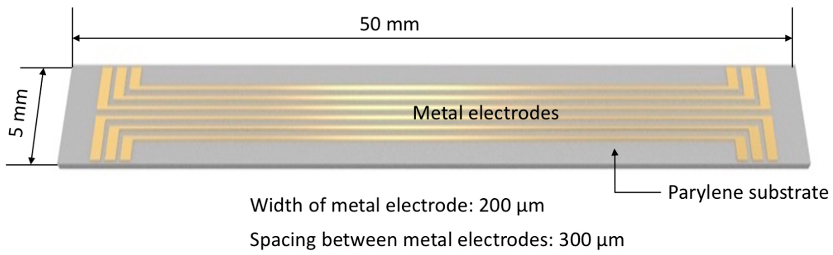
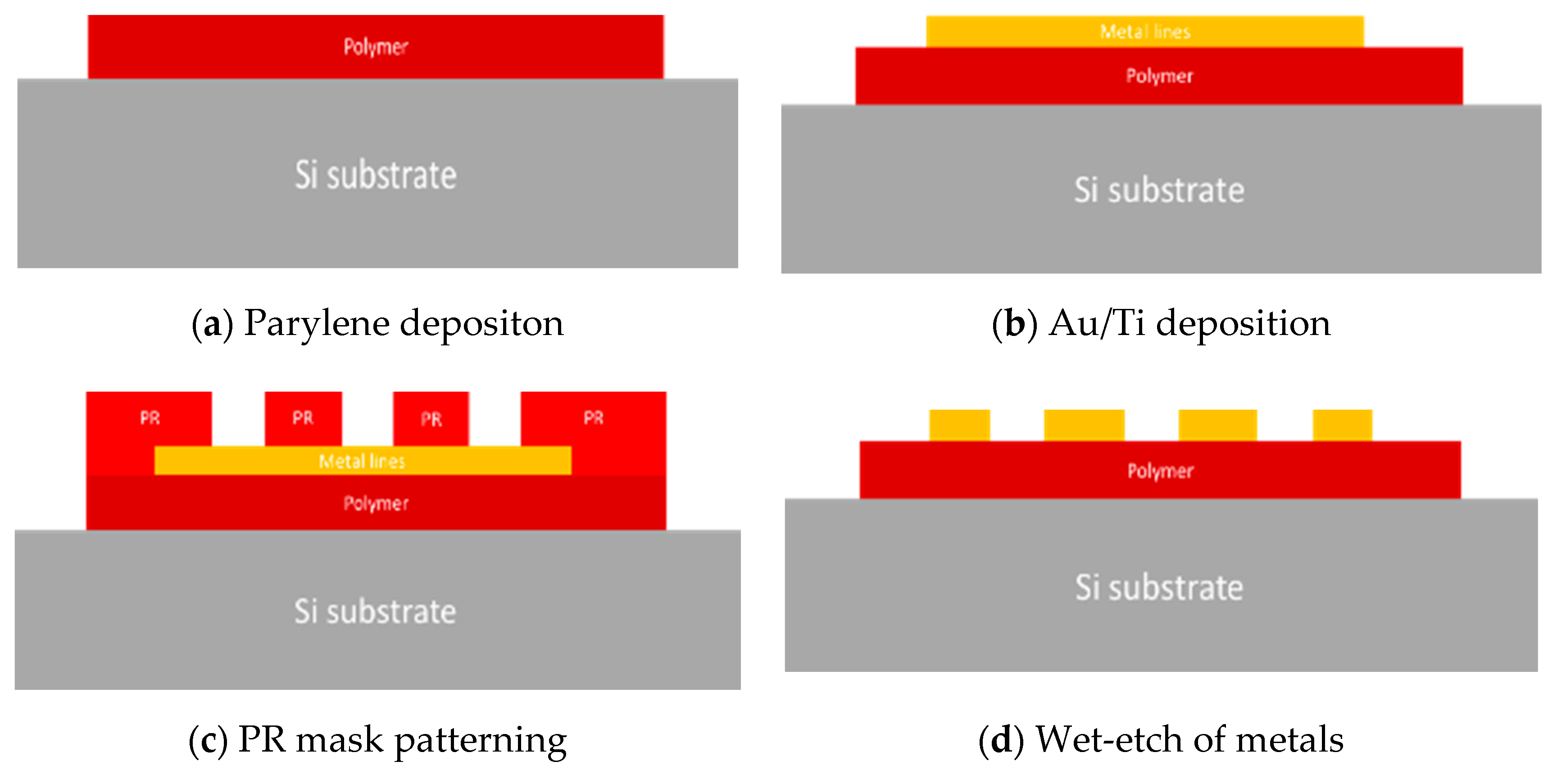
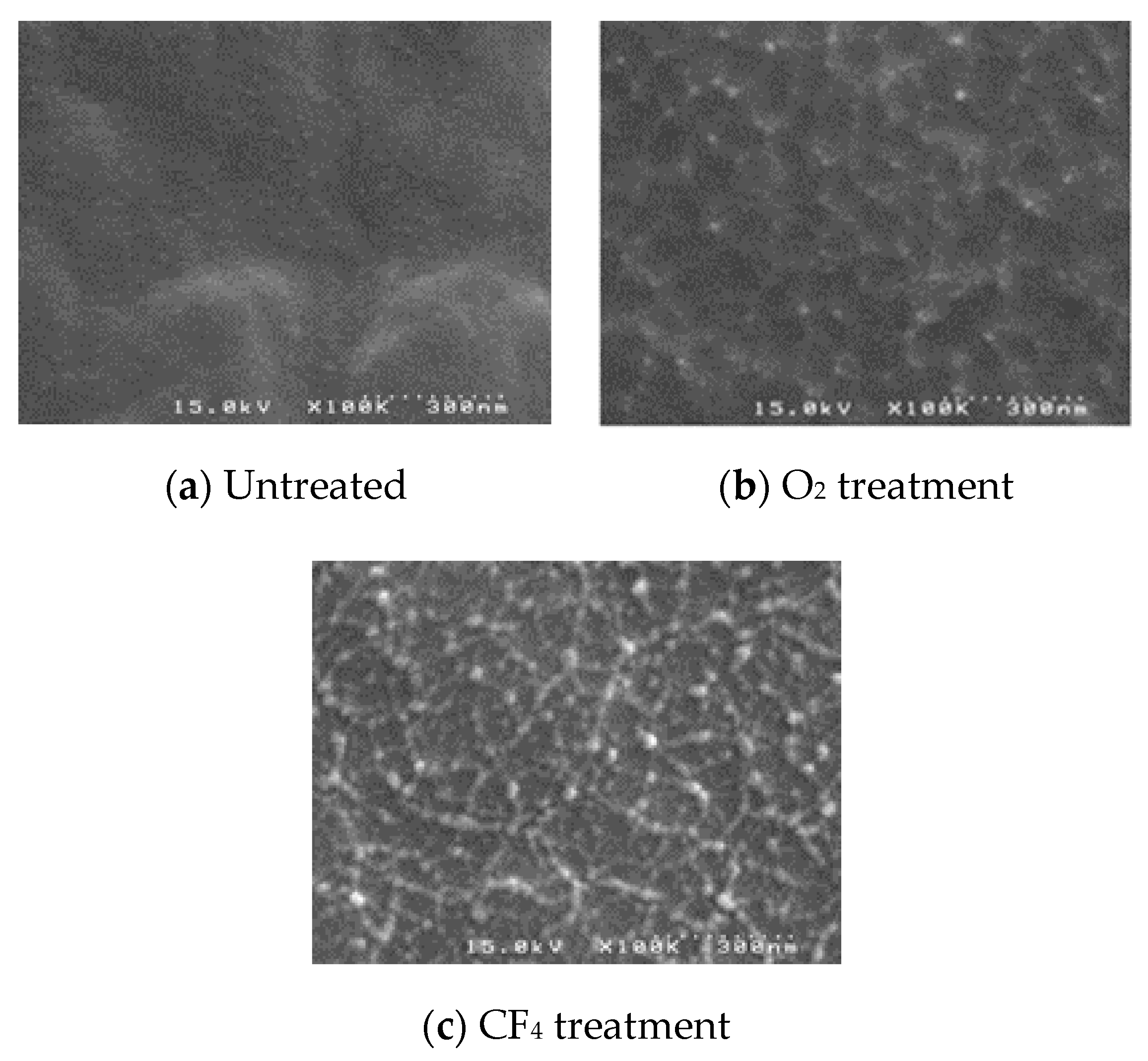
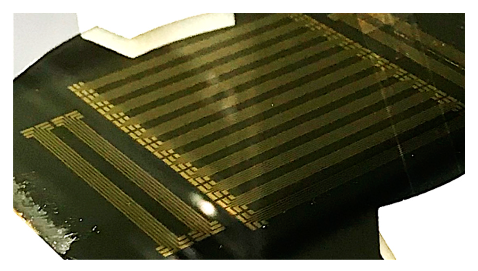
2. Test Sample Preparation for Metal Parylene Adhesion Test

Figure 1 shows the schematic of test pattern; it has length of 50 mm and width of 5 mm. It consists of 6 metal lines; each metal line has 200 µm in width and is spaced at 300 µm as is the design of multi-channel neural probe. Test pattern fabrication process is shown in Figure 2; (a) A parylene (parylene-C) layer having 5 µm in thickness was deposited in a 4-inch Si wafer using by commercial parylene coater system (VPC-500, Paco Engineering, Incheon, Korea). The monomer was deposited on the surface of the silicon wafer at a vapor phase condition with 0.8 μm/min, and deposition temperature was 20 °C. (b) Before metal layers deposition, the parylene surface was etched with CF4 gas (process conditions; (25 mTorr, 20 sccm, 1.5 min)) without O2 in order to increase surface roughness reducing the hydrophobicity, as shown in Figure 3. Note that O2 was not used for surface modification since the parylene is susceptible to be surface oxidation causing degradation of mechanical properties of the polymer neural probe. Moreover, the nanopillar structures on parylene substrate was efficiently built with CF4 gas rather than O2 gas, as shown in Figure 3b,c. Besides, there have been two major methods to improve interfacial adhesion between parylene and metal layer: chemical treatment or mechanical surface modification with RIE (Reactive Ion Etching) etch (Plasma-therm 790 MF, Plasma-Therm, Saint Petersburg, FL, USA). Concerning the test sample used in our study, parylene was already deposited on a silicon substrate; thus, chemical treatment may have changed the properties of parylene substrate itself, as well as the interface on which the metal was deposited. Furthermore, RIE etch have shown better performance compared with conventional A-174 saline chemical treatment [15]. Therefore, we modified the parylene surface with CF4 plasma etch to make a nanopillared surface, increasing the interfacial energy. The effectiveness of the nanopillared parylene surface was confirmed during metal patterning step. Titanium (30 nm) and gold (300 nm) were sequentially deposited with using by E-beam evaporator (ei5, ULVAC, Methuen MA, USA) on the parylene substrate without rupture of vacuum. (c) Photoresist (AZ GXR 601 (46cp), Merck, Kenilworth, NJ, USA) was patterned as a metal etch mask. The process conditions are summarized in Table 1. (d) Gold was first etched with Au etchant (Gold ETCH TFA, Transene Company, Danvers, MA, USA) for 5 min, and then titanium is etched with BOE (Buffered Oxide Etchant) solution (Buffered oxide etch 6:1, VWR International, Radnor, PA, USA) for 10 s. After metal patterning, PR mask was removed with acetone. Etch time was 60 s.
Resultant test samples on 4-inch silicon wafer is shown in Figure 4. All of metal lines were successfully implemented on the parylene substrate without any delamination during etching process. Note that the metal lines were fully delaminated from the parylene substrate during metal wet-etch step.

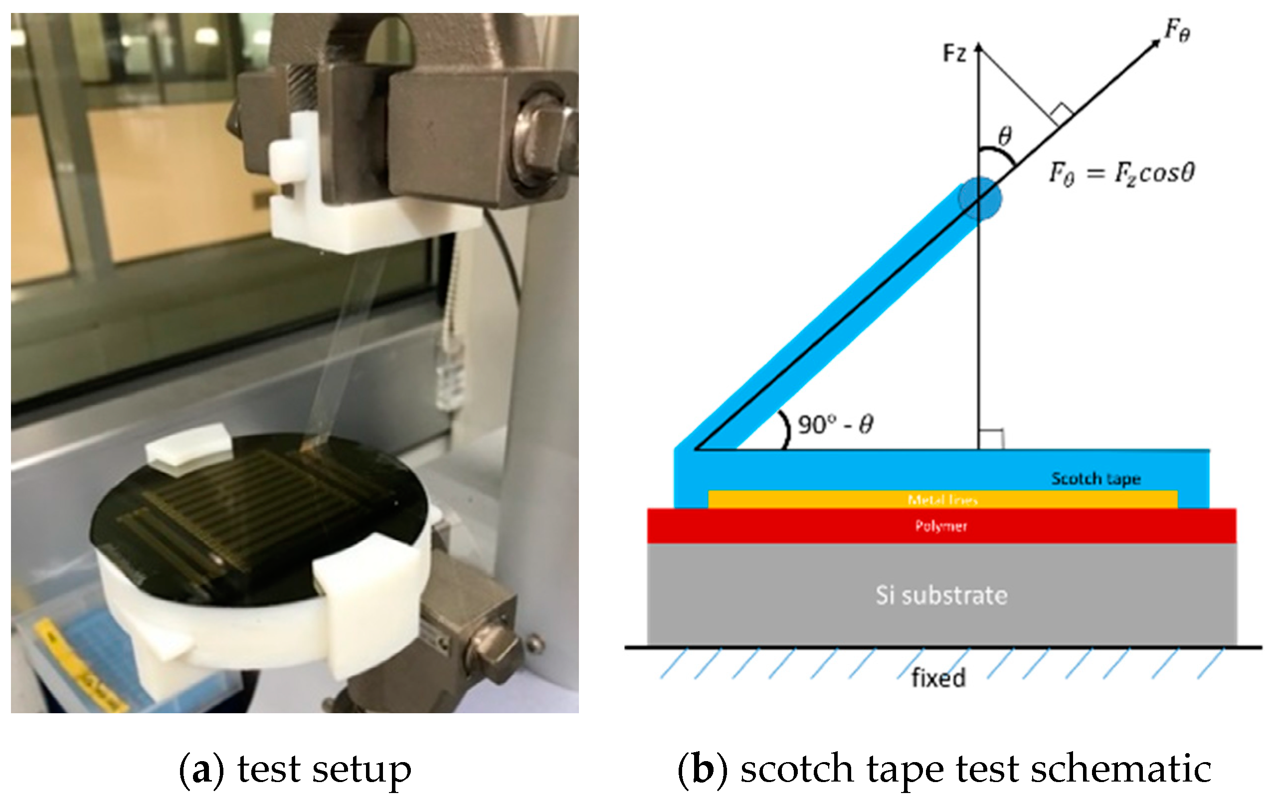
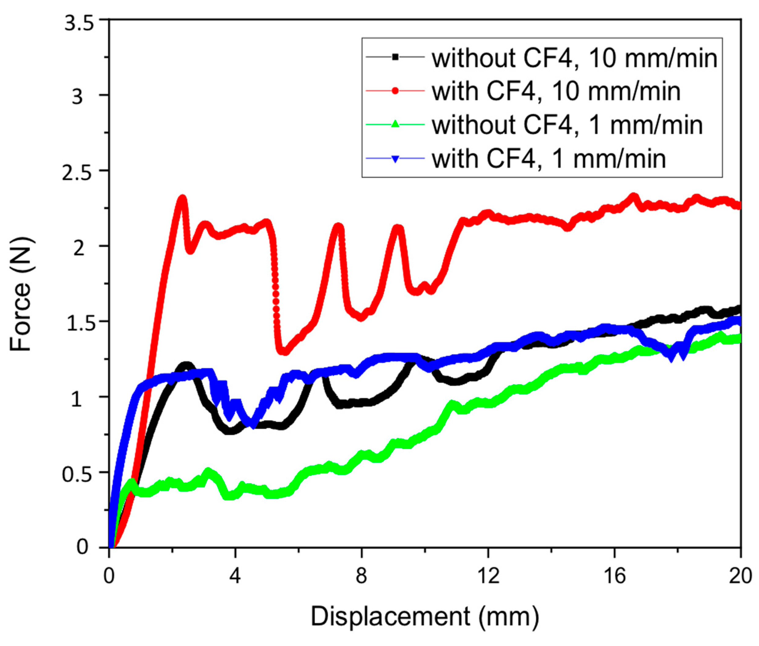
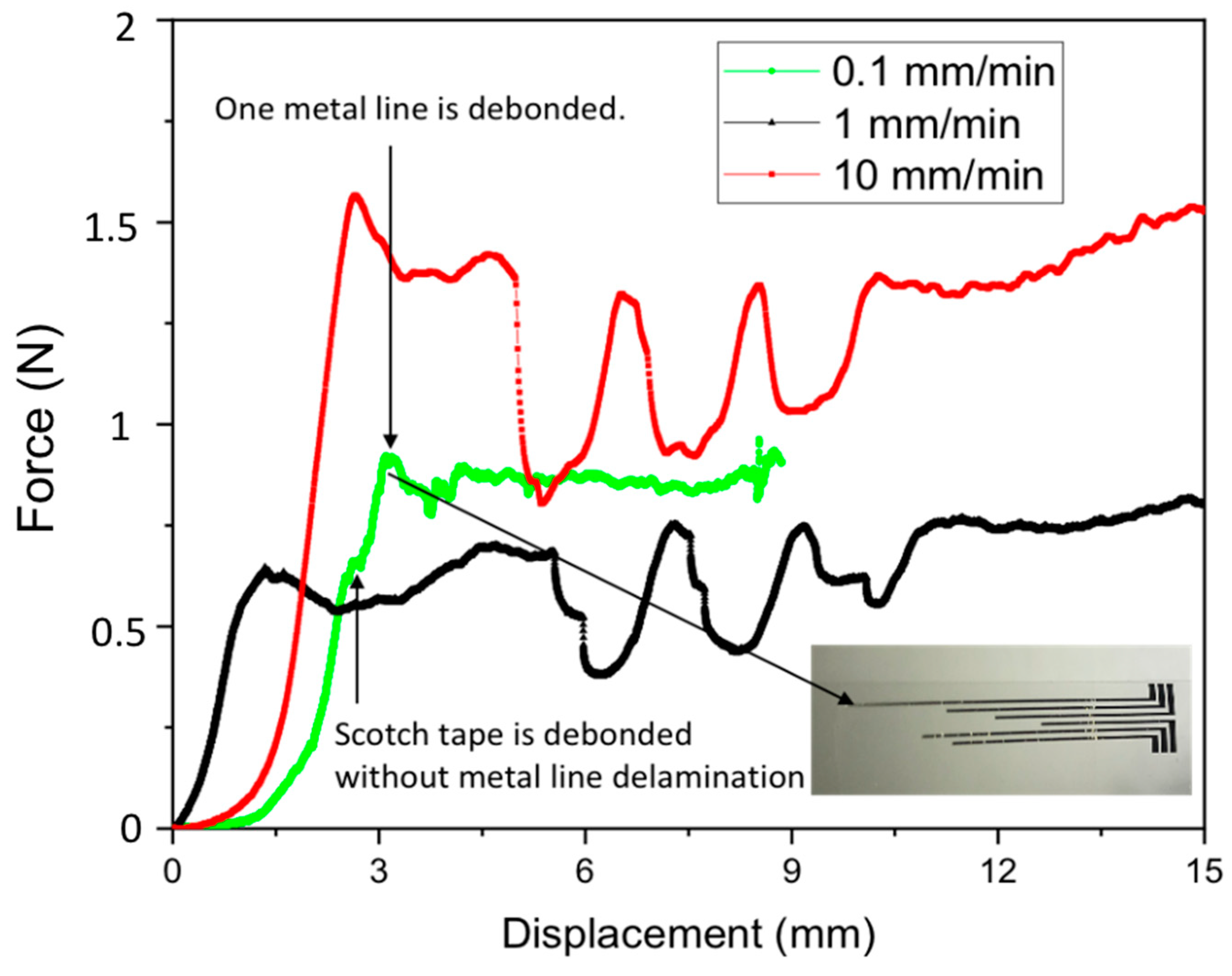
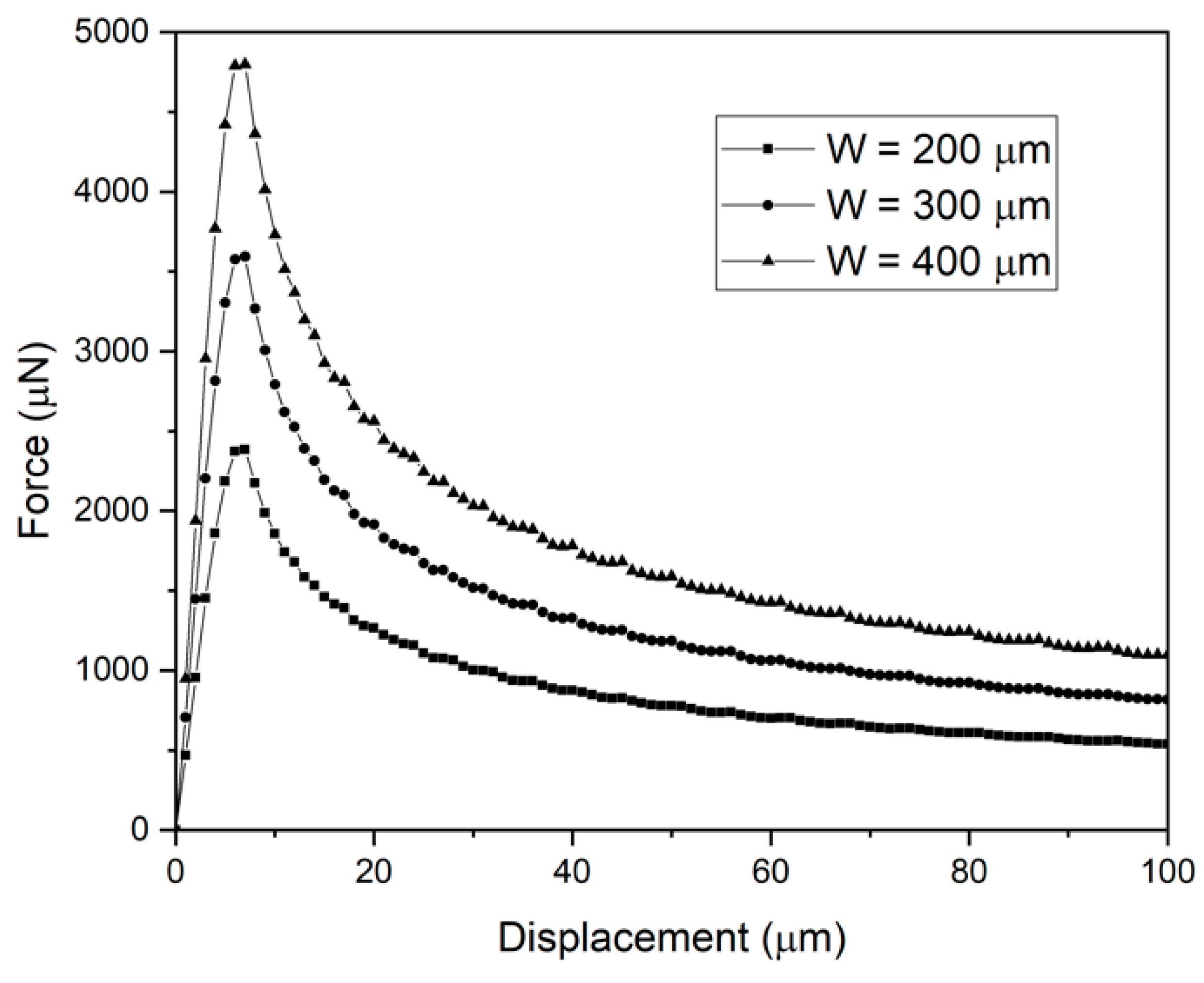
3. Scotch Tape Test for Metal Adhesion to Parylene Substrate

The prepared test samples underwent the scotch tape test to evaluate adhesion strength of the metal electrodes to the parylene substrate. The machine used for the scotch tape test was Shimadzu EZ-S machine (Shimadzu, Kyoto, Japan) dedicated for tensile testing. Figure 5 shows a photo of scotch tape attached on the test sample and schematics of the scotch tape test, respectively. The scotch tape is 3 M transparent tape 550. It has thickness of 50 μm and 12 mm width, and it provides adhesion to steel of 1.8 N/cm (or 0.18 N/mm).
Referring to Figure 5b, the scotch tape test was carried out in the following way; the machine applies stroke (unit: mm/min) into one end of the scotch tape, and then it measures force Fz (unit: N). As force of interest is Fθ, relationship between Fz and Fθ can be calculated as Equation (1).
F θ = F z c o s   θ .
During the scotch tape test, the angle (90°−θ) was changed from 60° to 90°; thus, Fθ = 0.5 Fz at 45°, and Fθ = Fz at 90°. For simplicity, we used the measured Fz from the scotch tape test to extract the adhesion strength.
Metal adhesion to parylene substrate was then measured with the scotch tape test. Scotch tape was attached to the parylene surface, slightly away from the left-end metal line to the right-end of the metal. After that, two different strokes (10 mm/min and 1 mm/min) were applied to the scotch tape, and corresponding force was measured as shown in Figure 6. All metal lines were debonded from the parylene substrate for all the cases. It was found that the sample with CF4 treatment needs more force than that without CF4 treatment, which means a parylene surface with CF4 treatment sticks better to scotch tape. This is a proof that parylene surface energy can be increased with only CF4 treatment without O2.
The first peak in each measured force was due to initiation of metal debonding, which makes abrupt drop of force. Minimal adhesion force is found when a stroke of 1 mm/min was applied to the parylene test sample without CF4 treatment (green line). It can be said that the metal adhesion had lower than the adhesion value estimated from the first peak. The adhesion can be calculated as follows; (0.5 N/12 mm) × (1.2 mm/12 mm) = 4.2 N/m. As all metal lines were debonded, the metal adhesion should have had lower than 4.2 J/m2. Thus, a lower stoke of 0.1 mm/min was applied to find metal adhesion to the parylene substrate. In this case, the scotch tape was attached only to the narrow metal lines of CF4 treated parylene and then force was recoded while stroke of 0.1 mm/min is applied. The measured force-displacement curve was compared with the previous results of 1 mm/min and 10 mm/min, as shown in Figure 7. As remarked in Figure 7, the scotch tape was debonded up to 0.9 N without metal line delamination, and one metal line started to debond from 0.91 N. Therefore, metal adhesion could be extracted from this peak force; (0.91 N/12 mm) × (0.2 mm/12 mm) = (76 N/m) × (0.017) = 1.29 N/m = 1.29 J/m2. Note that inset shows transferred metal lines on the scotch tape. Scotch tape strokes of 1 mm/min and 10 mm/min introduced large force fluctuation, which would result from relatively large applied force compared with interfacial energy.
Table 2 summarizes adhesion force between parylene and metal layer of previous reports compared with this work. The majority of the studies on metal-parylene adhesion force deal with parylene layer deposited on metal film with inteface treatment. Thus, they can provide from tens N/m to hundreds N/m of adhesion force. A thin metal layer, like Al thin film, on PET(Polyethylene terephthalate) layer has 46.7 N/m of adhesion. The thin gold metal line of this work had 1.29 N/m of adhesion force, which may result from the relatively narrow metal line of 200 μm.

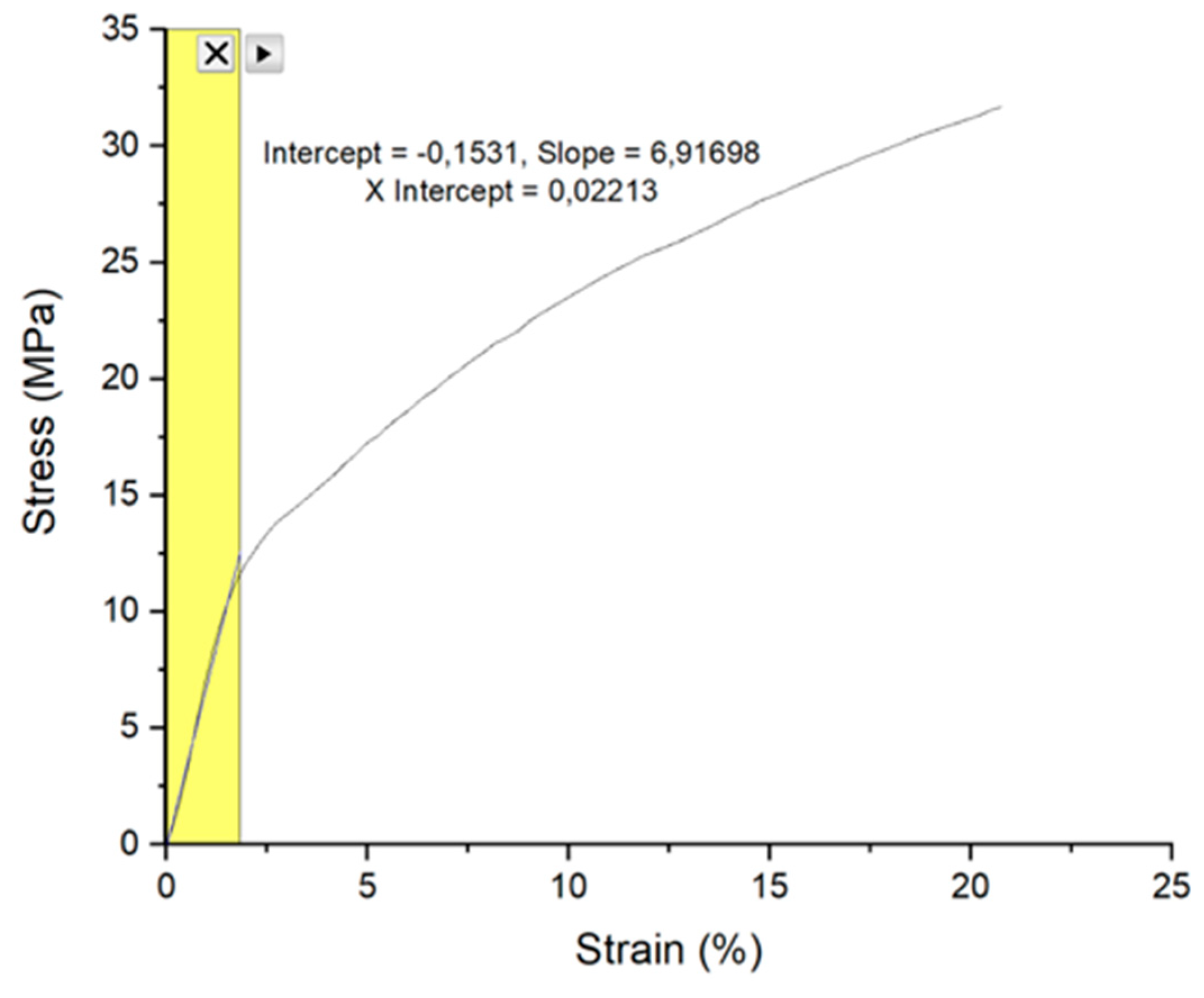
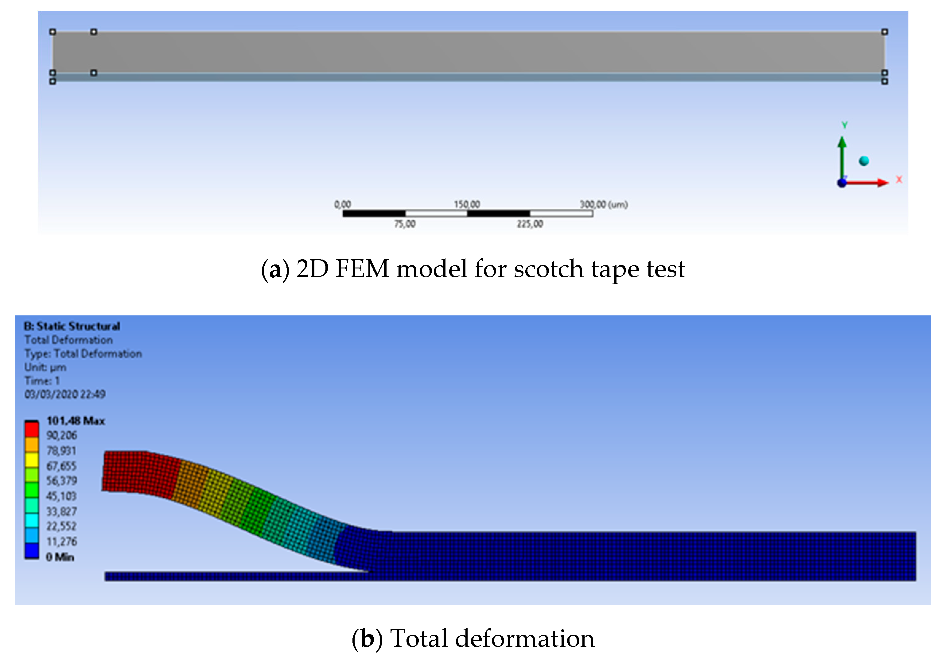
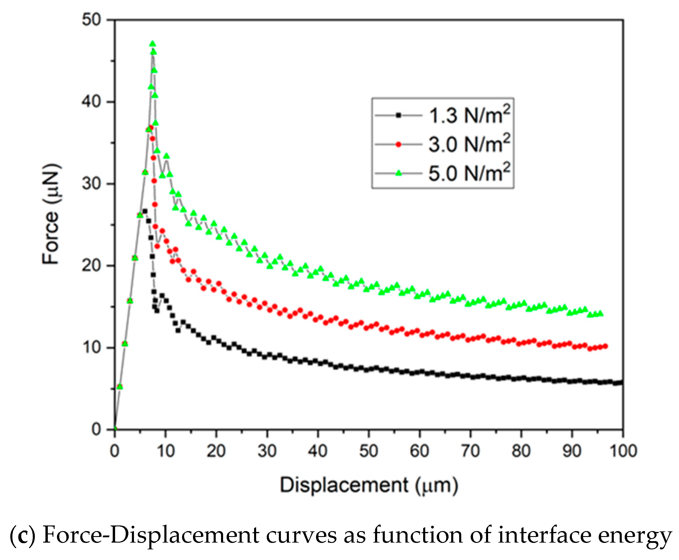
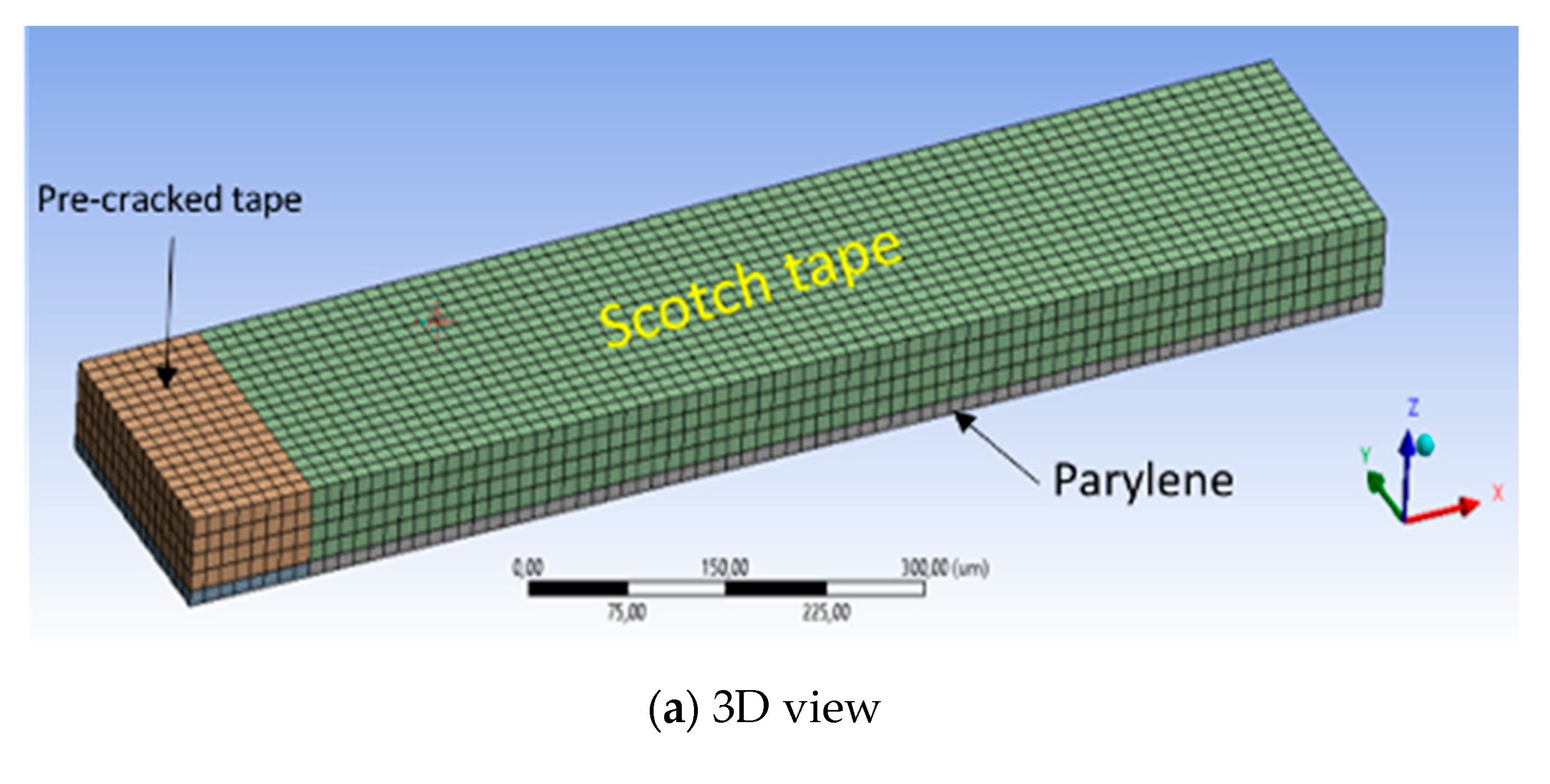
4. FEM Modeling and Simulation

FEM modeling and simulation is very useful to understand stress effect and corresponding deformation of MEMS package, debonding characteristics of a transfer packaging, and mechanical behaviors related with delamination [23,24,25,26,27]. Especially, debonding of a substrate and film delamination can be studied by adopting a CZM (Cohesive Zone model) to represent the interface of interest [28,29,30].
For FEM modeling, material properties of each element are important to get good simulation results. Required material properties in this modeling are Young’s moduli and poisson ratios of scotch tape and parylene and strain energy release rate of interface between the scotch tape and parylene. Young’s modulus of the scotch tape is extracted from tensile test result, as shown in Figure 8. The Young’s modulus of the scotch tape is 6.9 MPa in the elastic region, and the maximum applied force in the elastic region is 7.6 N when the applied strain is 2.2% (2.2 mm elongation as test scotch tape length is 100 mm). From the tensile test result, scotch tape in the metal adhesion test would be in the elastic region as the applied force is less than 2 N in all the cases. Poisson ratio of the scotch tape is assumed to be 0.4 as other polymer materials. Young’s modulus and poisson ratio of parylene are 2.67 GPa, as extracted in previous work, and 0.4, respectively [23]. Table 3 summarizes material properties for the FEM model. Note that interface material properties were defined with critical strain energy release rate. The value for critical strain energy release rate was the measured adhesion force as explained earlier.
Given with material properties, modeling and simulation of the scotch tape test was performed in two steps: 1) crack propagation behavior of the interface between the scotch tape and parylene substrate 2) debonding of the scotch tape from parylene substrate based on CZM.
A 2D FEM model for crack propagation was built, as shown in Figure 9a. The length of this model was 1000 µm, and thickness was 50 µm for scotch tape and 5 µm for parylene polymer. The following boundary conditions were applied: bottom line is fixed and displacement load is applied to left-top end, having 50 µm width. Note that 2D model behavior was defined as plane strain. Total deformation of the model when displacement of 100 μm in y direction was applied to the scotch tape is presented in Figure 9b. As is in the scotch tape test, delamination of the interface between scotch tape and parylene occurred, and crack propagated in x-direction.
Force-displacement was investigated as function of interface adhesion energy, as shown in Figure 9c. The required force for crack initiation was increased as interface adhesion energy increased, as expected. The force magnitude smaller than the measurement would have been due to thickness effect in 2D simulation. An important parameter in this graph is minimal displacements for crack initiation: 5 µm, 6.7 μm, and 7.6 μm for 1.3 N/m2, 3.0 N/m2, and 5.0 N/m2, respectively. These parameters are included in the following 3D interface delamination as a part of CZM parameters. From the simulation results, strain energy release rate (SERR) for mode 1 referring to VCCT (Virtual Crack Closure Technique) (G1), SERR for mode 2 from VCCT (G2), and SERR for mode 3 from VCCT (G3) were found 0.5 J/m2, 0.75 J/m2 and 0 J/m2, respectively. The total amount of VCCTs corresponded to the interface energy of 1.3 N/m2. Principal modes of the fracture of the delamination was from mode 1 and mode 2.
Figure 10a shows 3D model for the CZM interface delamination. As indicated in Figure 10b, there were two different regions in this model: pre-cracked (interface I) and CZM-modeled (interface II). CZM is a useful way to simulate interface delamination, which is frequently used for thin film delamination and transfer packaging technique [24,25]. The interface II, which is of interest for the adhesion, is modeled with CZM (Cohesive Zone Model) parameters, as explained in Figure 10c. As the bilinear CZM model needs at least two parameters, maximum normal traction and normal displacement at debonding was defined, as presented in Table 4. The minimal gaps for the fracture initiation found from the previous crack propagation simulation were included for 3D CZM simulation to estimate applied force to initiate the interface crack.
A displacement load was applied to one-end of the scotch tape, and then the force-displacement was extracted from the simulation. Referring to bilinear CZM model, critical strain energy release rate was calculated 1.25 J/m2. Initial width of the 3D model was 200 µm as was the fabricated metal electrode width. As in the 2D case, displacement load was applied to left-tip end. Extracted force-displacement curve at the loading place is presented in Figure 11. Minimal force for debonding of scotch tape was estimated 1.2 N/m, while measured one was 1.29 N/m. Adhesion force of the simulation had a good agreement with the measurement. Width of metal electrode could have been increased to get larger interface adhesion, as shown in Figure 11 When wider metal electrode is used to achieve larger metal-parylene adhesion, metal line impedance for neural signal acquisition should be taken into account.

5. Conclusions

Thin film flexible polymeric devices, such as a parylene-metal-parylene system, are being used for measuring nerve impulse from the central or peripheral nerve systems. Such thin-film polymeric devices provide advantages of flexibility and biocompatibility, but they are prone to delamination and carry concerns about their mechanical robustness. Therefore, metal adhesion strength to polymer substrate is important. The adhesion of metal electrodes to parylene substrate was measured by the scotch tape test. Thin and long metal electrodes was patterned on a parylene substrate in which the surface was modified by CF4 plasma etch before the metal deposition through e-beam evaporation. Metal adhesion strength was estimated by measuring force-displacement curve of the scotch tape test. The estimated metal adhesion was 1.3 J/m2. Experiment result was verified through FEM modeling of the scotch tape test. The proposed modeling method provided adhesion force having good agreement with experimental result. Although a thin-film parylene-based device can provide excellent short-term reliability, there exists one significant drawback of poor adhesion to metallic layer. The failure of the metal electrode on the parylene substrate is accelerated in the wet environment of a human body and under mechanical forces originating from body movement. Therefore, mechanical integrity in conditions of a human body implant or movement will be performed to assess long-term reliability of the parylene-metal devices, along with the biocompatibility of the parylene-base neural probe.

Author Contributions

Conceptualization, S.S. and J.K.; methodology, H.P.; software, H.P.; validation, S.S., H.P. and J.K.; formal analysis, S.S.; investigation, H.P.; resources, H.P.; data curation, H.P.; writing—original draft preparation, S.S.; writing—review and editing, S.S.; visualization, S.S.; supervision, J.K.; project administration, J.K.; funding acquisition, J.K. All authors have read and agreed to the published version of the manuscript.

Funding

This research was supported by the convergence technology development program for bionic arm through the National Research Foundation of Korea (NRF) funded by the Ministry of Science & ICT (No. 2017M3C1B2085292). This work was also supported by the Korea Institute of Science and Technology institutional program (2E30090 and 2V08590).

Conflicts of Interest

The authors declare no conflict of interest.

References

  1. Anderson, D.J.; Najafi, K.; Tanghe, S.J.; Evans, D.A.; Levy, K.L.; Hetke, J.F.; Xue, X.; Zappia, J.J.; Wise, K.D. Batch-fabricated thin-film electrodes for stimulation of the central auditory system. IEEE Trans. Biomed. Eng. 1989, 36, 693–704. [Google Scholar] [CrossRef] [PubMed]
  2. Campbell, P.K.; Normann, R.A.; Horch, K.W.; Stensaas, S.S. A chronic intracortical electrode array: Preliminary results. J. Biomed. Mater. Res. Appl. Biomat. 1989, 23, 245–259. [Google Scholar]
  3. Eichenbaum, H.; Kuperstein, M. Extracellular neural recording with multichannel microelectrodes. J. Electrophysiol. Tech. 1986, 13, 189–209. [Google Scholar]
  4. Najafi, K.; Ji, J.; Wise, K.D. Scaling limitation on silicon multichannel recoding probe. IEEE Trans. Biomed. Eng. 1990, 37, 1–11. [Google Scholar] [CrossRef]
  5. Campbell, P.K.; Jones, K.E.; Huber, R.J.; Horch, K.W.; Normann, R.A. A silicon-based, three-dimensional neural interface: Manufacturing processes for an intracortical electrode array. IEEE Trans. Biomed. Eng. 1991, 38, 758–768. [Google Scholar] [CrossRef]
  6. Takeuchi, S.; Suzuki, T.; Mabuchi, K.; Fujita, H. 3D flexible multichannel neural probe array. J. Micromechanics Microengineering 2004, 14, 104–107. [Google Scholar] [CrossRef]
  7. Kim, O.; Choi, W.; Jung, W.; Jung, S.; Park, H.; Park, J.W.; Kim, J. Novel Neural Interface Electrode Array for the Peripheral Nerve. In Proceedings of the International Conference on Rehabilitation Robotics (ICORR), London, UK, 17–20 July 2017. [Google Scholar]
  8. Castagnola, V.; Descamps, E.; Lecestre, A.; Dahan, L.; Remaud, J.; Nowak, L.G.; Bergaud, C. Parylene-based flexible neural probes with PEDOT coated surface for brain stimulation and recording. Biosens. Bioelectron. 2015, 67, 450–457. [Google Scholar] [CrossRef]
  9. Cheung, K.C.; Renaud, P.; Tanila, H.; Djupsund, K. Flexible Polyimide Microelectrode Array for in Vivo Recordings and Current Source Density Analysis. Biosens. Bioelectron. 2007, 22, 1783–1790. [Google Scholar] [CrossRef] [Green Version]
  10. Stieglitz, T. Development of a micromachined epiretinal vision prosthesis. J. Neural Eng. 2009, 6, 065005. [Google Scholar] [CrossRef] [Green Version]
  11. Ordonez, J.; Schuettler, M.; Boehler, C.; Boretius, T.; Stieglitz, T. Thin films and microelectrode arrays for neuroprosthetics. MRS Bull. 2012, 37, 590–598. [Google Scholar] [CrossRef] [Green Version]
  12. Chen, Z.; Ryzhik, L.; Palanker, D. Current Distribution on Capacitive Electrode-Electrolyte Interfaces. Phys. Rev. Appl. 2020, 13. [Google Scholar] [CrossRef] [Green Version]
  13. Onzález, C.; Rodríguez, M. A flexible perforated microelectrode array probe for action potential recording in nerve and muscle tissues. J. Neurosci. Methods 1997, 72, 189–195. [Google Scholar] [CrossRef]
  14. Lee, C.D.; Meng, E. Mechanical properties of thin-film Parylene- metal-Parylen devices. Front. Mech. Eng. 2015, 1, 10. [Google Scholar] [CrossRef] [Green Version]
  15. Xie, Y.; Pei, W.; Guo, D.; Zhang, L.; Zhang, H.; Guo, X.; Xing, X.; Yang, X.; Wang, F.; Gui, Q.; et al. Improving adhesion strength between layers of an implantable parylene-C electrode. Sens. Actuators A Phys. 2017, 260, 117–123. [Google Scholar] [CrossRef]
  16. Oliva, N.; Mueller, M.; Stieglitz, T.; Navarro, X.; del Valle, J. On the use of Parylene C polymer as substrate for periphral nerve electrode. Sci. Rep. 2018, 8, 1–12. [Google Scholar]
  17. Chang, J.H.; Lu, B.; Tai, Y.C. Adhesion-enhancing surface treatments for parylene deposition. In Proceedings of the International Solid-State Sensors, Actuators and Microsystems Conference (Transducers 2011), Beijing, China, 5–9 June 2011. [Google Scholar]
  18. Jesdinszki, M.; Struller, C.; Rodler, N.; Blondin, D.; Cassio, V.; Kucukpinar, E.; Langowski, H.-C. Evaluation of Adhesion Strength Between Thin Aluminum Layer and Poly(ethylene terephthalate) Substrate by Peel Tests—A Practical Approach for the Packaging Industry. J. Adhes. Sci. Technol. 2012, 26, 2357–2380. [Google Scholar] [CrossRef]
  19. Tsai, L.-C.; Rezaee, M.; Haider, M.I.; Yazdi, A.; Salowitz, N.P. QUANTITATIVE MEASUREMENT OF THIN FILM ADHESION FORCE. In Proceedings of the ASME 2019 Conference on Smart Materials, Adaptive Structures and Intelligent Systems SMASIS 2019, Louisville, KY, USA, 9–11 September 2019. [Google Scholar]
  20. Min, K.; Rammohan, A.R.; Lee, H.S.; Shin, J.; Lee, S.H.; Goyal, S.; Park, H.; Mauro, J.C.; Stewart, R.; Botu, V.; et al. Computational approaches for investigating interfacial adhesion phenomena of polyimide on silica glass. Sci. Rep. 2017, 7, 10475. [Google Scholar] [CrossRef] [Green Version]
  21. ASTM-D-3359. Standard Test Methods for Measuring Adhesion by Tape Test; ASTM International: West Conshohocken, PA, USA, 2010. [Google Scholar]
  22. Yamagishi, F.G. Investigations of plasma-polymerized films as primers for Parylene-C coatings on neural prosthesis materials. Thin Solid Film. 1991, 202, 39–50. [Google Scholar] [CrossRef]
  23. Seok, S.; Park, H.D.; Choi, W.; Kim, O.; Kim, J. Analysis of Thin Film Parylene-Metal-Parylene Device Based on Mechanical Tensile Strength Measurement. In Proceedings of the DTIP 2019, Berlin, Germany, 8–12 September 2019. [Google Scholar]
  24. Lishchynska, M.; O’Mahony, C.; Slattery, O.; Wittler, O.; Walter, H. Evaluation of Packaging Effect on MEMS Performance: Simulation and Experimental Study. IEEE Trans. Adv. Packag. 2007, 30, 629–635. [Google Scholar] [CrossRef]
  25. Seok, S.; Rolland, N.; Rolland, P.-A. A Theoretical and Experimental Study of BCB Thin-Film Cap Zero-Level Package Based on FEM Simulations. J. Micromechanics Microengineering 2010. [Google Scholar] [CrossRef]
  26. Seok, S. A Theoretical Study on Post-it-like Debonding Process for BCB Cap Transfer Packaging Based on FEM Simulation. IEEE Trans. Compon. Packag. Manuf. Technol. CPMT 2015, 5, 1417–1422. [Google Scholar] [CrossRef]
  27. Seok, S. Fabrication and Modeling of Nitride Thin Film Encapsulation Based on Anti-Adhesion-Assisted Transfer Technique and Nitride/BCB Bilayer Wrinkling. IEEE Trans. Compon. Packag. Manuf. Technol. CPMT 2016, 6, 1301–1307. [Google Scholar] [CrossRef]
  28. Yan, Y.; Shang, F. Cohesive zone modeling of interfacial delamination in PZT thin films. Int. J. Solids Struct. 2009, 46, 2739–2749. [Google Scholar] [CrossRef] [Green Version]
  29. Samimi, M.; van Dommelen, J.A.W.; Geers, M.G.D. A three-dimensional self-adaptive cohesive zone model for interfacial delamination. Comput. Methods Appl. Mech. Eng. 2011, 200, 3540–3553. [Google Scholar] [CrossRef]
  30. Moslemi, M.; Khoshravan, M. Cohesive Zone Parameters Selection for Mode-I Prediction of Interfacial Delamination. J. Mech. Eng. 2015, 61, 507–516. [Google Scholar] [CrossRef]
Figure 1. Design of test pattern.
Micromachines 11 00605 g001
Figure 2. Test sample fabrication process.
Micromachines 11 00605 g002
Figure 3. Parylene surface modification.
Micromachines 11 00605 g003
Figure 4. Test samples fabricated on 4-inch silicon substrate.
Micromachines 11 00605 g004
Figure 5. Scotch tape test for metal adhesion to parylene substrates.
Micromachines 11 00605 g005
Figure 6. Force-displacement curves from scotch tape test with metal lines on parylene substrate.
Micromachines 11 00605 g006
Figure 7. Force-displacement curves from scotch tape test with metal lines on parylene substrate with CF4 treatment.
Micromachines 11 00605 g007
Figure 8. Tensile test result of scotch tape.
Micromachines 11 00605 g008
Figure 9. Crack propagation model and simulation results.
Micromachines 11 00605 g009aMicromachines 11 00605 g009b
Figure 10. Three-dimensional Finite Element Method (FEM) model for Cohesive Zone model (CZM) interface delamination.
Micromachines 11 00605 g010aMicromachines 11 00605 g010b
Figure 11. Force-displacement curves as function of metal width.
Micromachines 11 00605 g011
Table 1. Photoresist etch mask process conditions.
StepConditions
PR coating10 s @1500 rpm
Soft bake60 s @ 95 °C
Exposure10 s @10 mW
Develop10 s @developer
Post exposure bake30 s @110 °C
Thickness1.2 μm
Table 2. Comparison of other research results with scotch tape test.
Test MethodTest Sample StructureInterface TreatmentEnvironmentRemarks
Adhesion Force
Peel 90° [18]Parylene (10 μm)/sputtered Ti (up to 100 nm)/Au (300 nm)/glass substrateGorham process before parylene deposition to make adhesion promoting layer48 h in PBS solutionmetal width = 10 mm
35.5 mN/mm
Peel 180° [19]Al thermal evaporated metal (60 nm)/PET (12 μm)/Al substrate (1 mm)-RTmetal width = 15 mm
0.7 N/15 mm
Tensile [15]Au (200 nm)/Cr (13 nm)/Parylene (10 μm)/glass substrateO2 RIE etchingRTmetal width = 15 mm
2.13 ± 0.12 MPa
Peel test [22]Parylene (9–20 μm)/Ti substratePlasma Polymerized Ethane (PPE)RTmetal width = NA
0.34 N/mm
Peel test [This work]Au(300 nm)/Ti(30 nm)/Parylene(5 μm)/Si substrateCF4 RIERTmetal width = 200 μm
1.29 N/m
Table 3. Material properties of materials and interface.
Material PropertiesScotch TapeParylene
Young’s modulus (Pa)6.9 × 1062.7 × 109
Poisson ratio0.40.4
-Interface
Critical mode I
energy release rate (J/m2)
1.3
Critical mode II
energy release rate (J/m2)
1.3
Critical mode III
energy release rate (J/m2)
1.3
Table 4. Cohesive Zone model (CZM) parameters.
Parameter NameValue
Maximum normal traction0.5 MPa
Normal displacement jump at completion of debonding5 µm
Maximum tangential traction0.5 MPa
Tangential displacement jump at completion of debonding5 µm

