Direct Write of 3D Nanoscale Mesh Objects with Platinum Precursor via Focused Helium Ion Beam Induced Deposition

 , ,
, ,  and
and
Abstract
:
1. Introduction
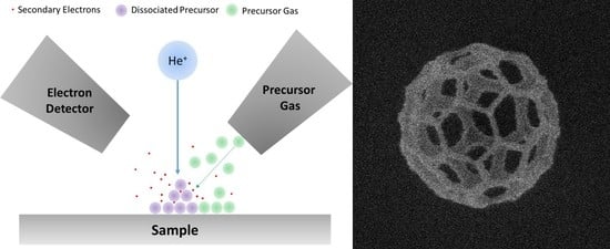
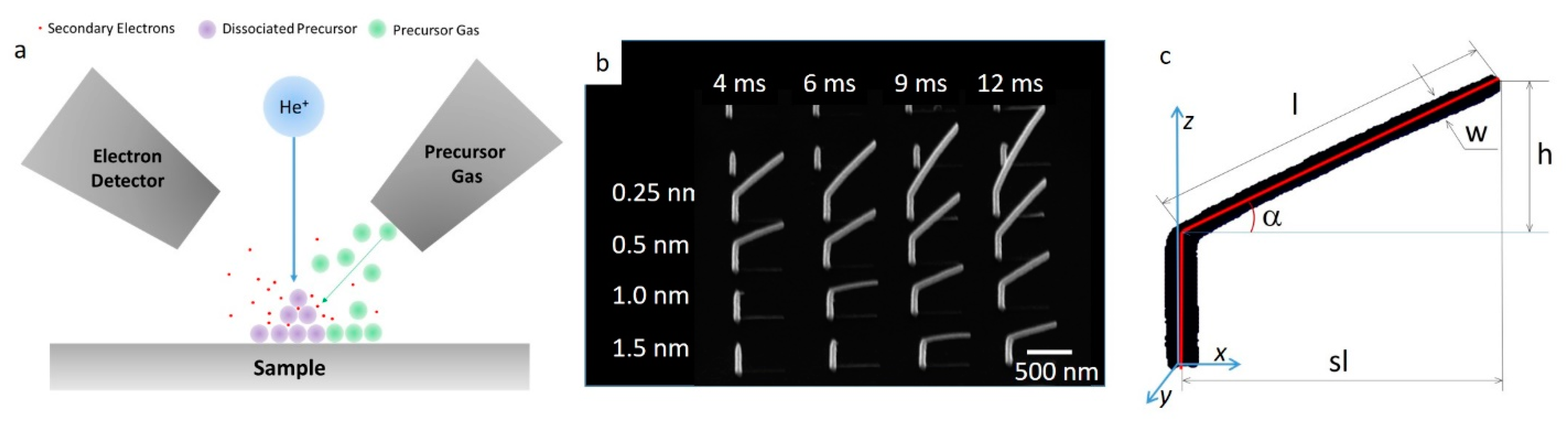
2. Experimental Methods
2.1. Growth
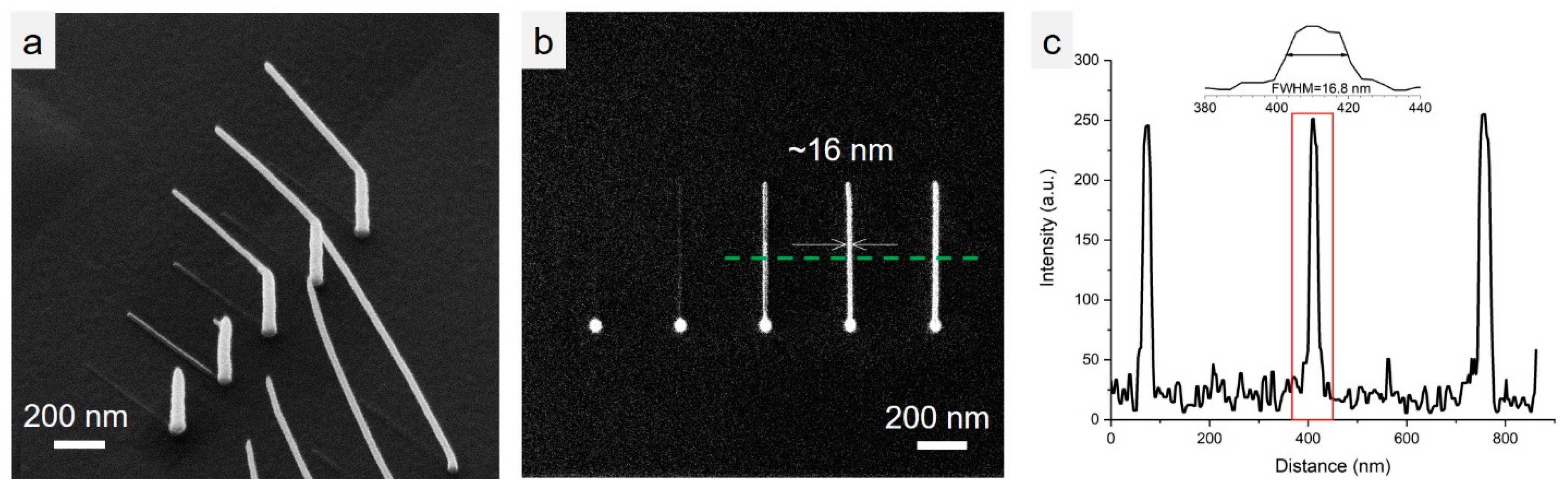
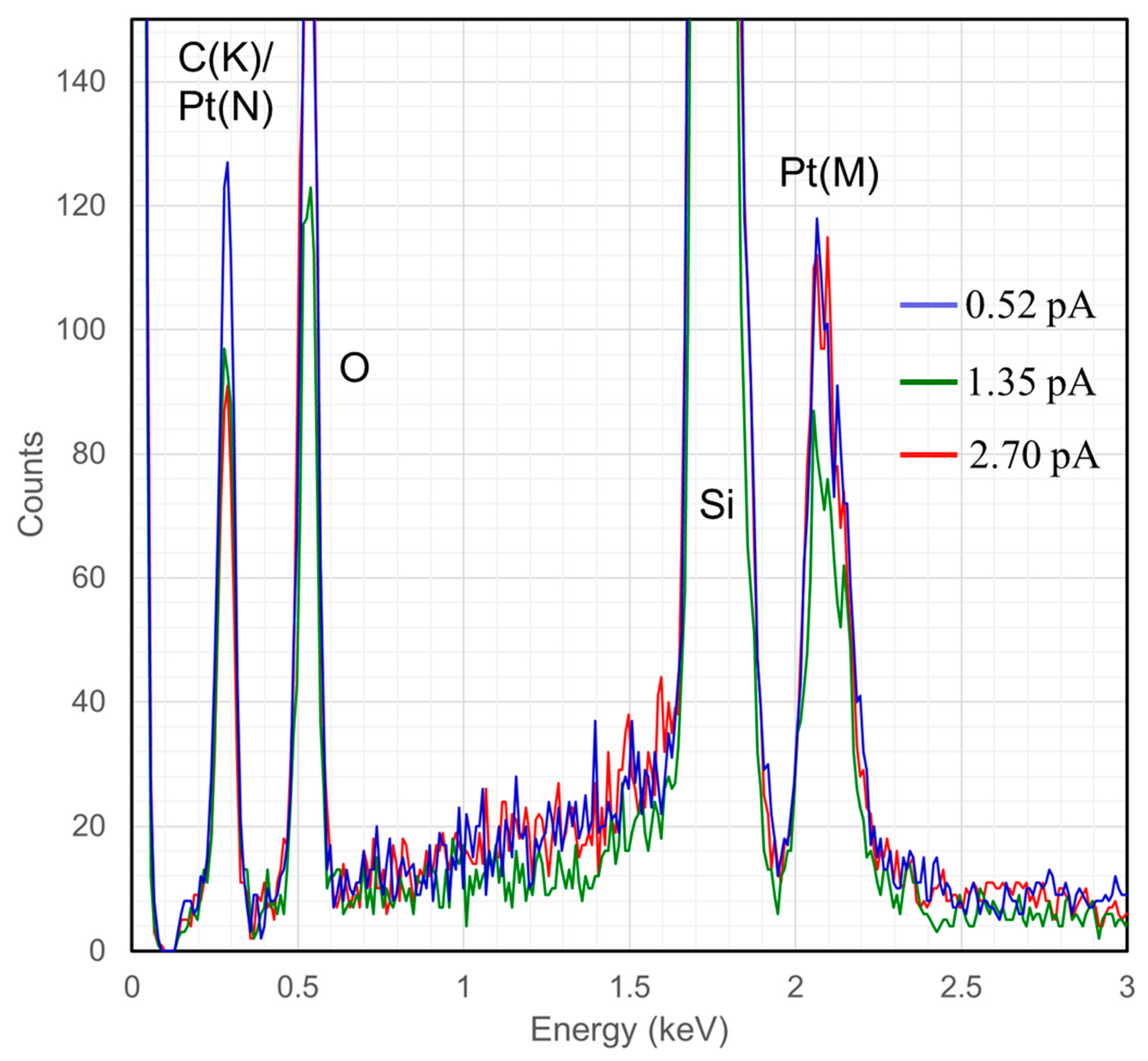
2.2. Data Analysis
3. Results and Discussion
Author Contributions
Funding
Conflicts of Interest
Notice
References
- Ito, T.; Okazaki, S. Pushing the Limits of Lithography. Nature 2000, 406, 1027–1031. [Google Scholar] [CrossRef]
- Harriott, L.R. Limits of Lithography. Proc. IEEE 2001, 89, 366–374. [Google Scholar] [CrossRef] [Green Version]
- Mack, C.A. Line-Edge Roughness and the Ultimate Limits of Lithography; SPIE Advanced Lithography, International Society for Optics and Photonics: San Jose, CA, USA, 2010; p. 763931. [Google Scholar]
- Broers, A.; Hoole, A.; Ryan, J. Electron Beam Lithography—Resolution Limits. Microelectron. Eng. 1996, 32, 131–142. [Google Scholar] [CrossRef]
- Van Dorp, W.F.; Zhang, X.; Feringa, B.L.; Hansen, T.W.; Wagner, J.B.; De Hosson, J.T.M. Molecule-by-Molecule Writing Using a Focused Electron Beam. ACS Nano 2012, 6, 10076–10081. [Google Scholar] [CrossRef] [Green Version]
- Jesse, S.; Borisevich, A.Y.; Fowlkes, J.D.; Lupini, A.R.; Rack, P.D.; Unocic, R.R.; Sumpter, B.G.; Kalinin, S.V.; Belianinov, A.; Ovchinnikova, O.S. Directing Matter: Toward Atomic-Scale 3d Nanofabrication. ACS Nano 2016, 10, 5600–5618. [Google Scholar] [CrossRef] [PubMed]
- Kankala, R.K.; Zhu, K.; Li, J.; Wang, C.-S.; Wang, S.-B.; Chen, A.-Z. Fabrication of Arbitrary 3d Components in Cardiac Surgery: From Macro-, Micro-to Nanoscale. Biofabrication 2017, 9, 032002. [Google Scholar] [CrossRef] [Green Version]
- Kim, C.-S.; Ahn, S.-H.; Jang, D.-Y. Developments in Micro/Nanoscale Fabrication by Focused Ion Beams. Vacuum 2012, 86, 1014–1035. [Google Scholar] [CrossRef]
- Grilli, S.; Coppola, S.; Vespini, V.; Merola, F.; Finizio, A.; Ferraro, P. 3d Lithography by Rapid Curing of the Liquid Instabilities at Nanoscale. Proc. Natl. Acad. Sci. USA 2011, 108, 15106–15111. [Google Scholar] [CrossRef] [Green Version]
- Cho, J.H.; Keung, M.D.; Verellen, N.; Lagae, L.; Moshchalkov, V.V.; Van Dorpe, P.; Gracias, D.H. Nanoscale Origami for 3d Optics. Small 2011, 7, 1943–1948. [Google Scholar] [CrossRef] [Green Version]
- Yee, D.W.; Schulz, M.D.; Grubbs, R.H.; Greer, J.R. Functionalized 3d Architected Materials Via Thiol-Michael Addition and Two-Photon Lithography. Adv. Mater. 2017, 29, 1605293. [Google Scholar] [CrossRef] [PubMed]
- Montemayor, L.C.; Meza, L.R.; Greer, J.R. Design and Fabrication of Hollow Rigid Nanolattices via Two-Photon Lithography. Adv. Eng. Mater. 2014, 16, 184–189. [Google Scholar] [CrossRef]
- Liontas, R.; Greer, J.R. 3d Nano-Architected Metallic Glass: Size Effect Suppresses Catastrophic Failure. Acta Mater. 2017, 13, 393–407. [Google Scholar] [CrossRef] [Green Version]
- Zocca, A.; Colombo, P.; Gomes, C.M.; Günster, J. Additive Manufacturing of Ceramics: Issues, Potentialities, and Opportunities. J. Am. Ceram. Soc. 2015, 98, 1983–2001. [Google Scholar] [CrossRef]
- Frazier, W.E. Metal Additive Manufacturing: A Review. J. Mater. Eng. Perform. 2014, 23, 1917–1928. [Google Scholar] [CrossRef]
- Hirt, L.; Reiser, A.; Spolenak, R.; Zambelli, T. Additive Manufacturing of Metal Structures at the Micrometer Scale. Adv. Mater. 2017, 29, 1604211. [Google Scholar] [CrossRef]
- Vyatskikh, A.; Delalande, S.; Kudo, A.; Zhang, X.; Portela, C.M.; Greer, J.R. Additive Manufacturing of 3d Nano-Architected Metals. Nat. Commun. 2018, 9, 593. [Google Scholar] [CrossRef]
- Ievlev, A.V.; Jakowski, J.; Burch, M.J.; Iberi, V.; Hysmith, H.; Joy, D.C.; Sumpter, B.G.; Belianinov, A.; Unocic, R.R.; Ovchinnikova, O.S. Building with Ions: Towards Direct Write of Platinum Nanostructures Using in Situ Liquid Cell Helium Ion Microscopy. Nanoscale 2017, 9, 12949–12956. [Google Scholar] [CrossRef]
- Unocic, R.R.; Lupini, A.R.; Borisevich, A.Y.; Cullen, D.A.; Kalinin, S.V.; Jesse, S. Direct-Write Liquid Phase Transformations with a Scanning Transmission Electron Microscope. Nanoscale 2016, 8, 15581–15588. [Google Scholar] [CrossRef]
- De Teresa, J.; Fernández-Pacheco, A. Present and Future Applications of Magnetic Nanostructures Grown by Febid. Appl. Phys. A 2014, 117, 1645–1658. [Google Scholar] [CrossRef]
- De Teresa, J.; Fernández-Pacheco, A.; Córdoba, R.; Serrano-Ramón, L.; Sangiao, S.; Ibarra, M.R. Review of Magnetic Nanostructures Grown by Focused Electron Beam Induced Deposition (Febid). J. Phys. D Appl. Phys. 2016, 49, 243003. [Google Scholar] [CrossRef]
- Wanzenboeck, H.; Hochleitner, G.; Mika, J.; Shawrav, M.; Gavagnin, M.; Bertagnolli, E. Mapping of Local Argon Impingement on a Virtual Surface: An Insight for Gas Injection During Febid. Appl. Phys. A 2014, 117, 1749–1756. [Google Scholar] [CrossRef] [Green Version]
- Van Dorp, W.; Hagen, C.W. A Critical Literature Review of Focused Electron Beam Induced Deposition. J. Appl. Phys. 2008, 104, 10. [Google Scholar] [CrossRef] [Green Version]
- Randolph, S.; Fowlkes, J.; Rack, P. Focused, Nanoscale Electron-Beam-Induced Deposition and Etching. Crit. Rev. Solid State Mater. Sci. 2006, 31, 55–89. [Google Scholar] [CrossRef]
- Utke, I.; Luisier, A.; Hoffmann, P.; Laub, D.; Buffat, P. Focused-Electron-Beam-Induced Deposition of Freestanding Three-Dimensional Nanostructures of Pure Coalesced Copper Crystals. Appl. Phys. Lett. 2002, 81, 3245–3247. [Google Scholar] [CrossRef]
- Bret, T.; Utke, I.; Bachmann, A.; Hoffmann, P. In Situ Control of the Focused-Electron-Beam-Induced Deposition Process. Appl. Phys. Lett. 2003, 83, 4005–4007. [Google Scholar] [CrossRef]
- Henry, M.R.; Kim, S.; Fedorov, A.G. High Purity Tungsten Nanostructures Via Focused Electron Beam Induced Deposition with Carrier Gas Assisted Supersonic Jet Delivery of Organometallic Precursors. J. Phys. Chem. C 2016, 120, 10584–10590. [Google Scholar] [CrossRef]
- Fedorov, A.G.; Kim, S.; Henry, M.; Kulkarni, D.; Tsukruk, V.V. Focused-Electron-Beam-Induced Processing (Febip) for Emerging Applications in Carbon Nanoelectronics. Appl. Phys. A 2014, 117, 1659–1674. [Google Scholar] [CrossRef]
- Fisher, J.S.; Kottke, P.A.; Kim, S.; Fedorov, A.G. Rapid Electron Beam Writing of Topologically Complex 3d Nanostructures Using Liquid Phase Precursor. Nano Lett. 2015, 15, 8385–8391. [Google Scholar] [CrossRef]
- Kim, S.; Henry, M.; Fedorov, A.G. Using an Energized Oxygen Micro-Jet for Improved Graphene Etching by Focused Electron Beam. Appl. Phys. Lett. 2015, 107, 233102. [Google Scholar] [CrossRef] [Green Version]
- Utke, I.; Hoffmann, P.; Melngailis, J. Gas-Assisted Focused Electron Beam and Ion Beam Processing and Fabrication. J. Vac. Sci. Technol. B Microelectron Nanometer Struct. Process. Meas. Phenom. 2008, 26, 1197–1276. [Google Scholar] [CrossRef] [Green Version]
- Alkemade, P.F.; Chen, P.; van Veldhoven, E.; Maas, D. Model for Nanopillar Growth by Focused Helium Ion-Beam-Induced Deposition. J. Vac. Sci. Technol. BNanotechnol. Microelectron. Mater. Process. Meas. Phenom. 2010, 28, C6F22–C26F25. [Google Scholar] [CrossRef] [Green Version]
- Boden, S.; Moktadir, Z.; Bagnall, D.; Mizuta, H.; Rutt, H. Focused Helium Ion Beam Milling and Deposition. Microelectron. Eng. 2011, 88, 2452–2455. [Google Scholar] [CrossRef]
- Drezner, Y.; Greenzweig, Y.; Fishman, D.; van Veldhoven, E.; Maas, D.J.; Raveh, A.; Livengood, R.H. Structural Characterization of He Ion Microscope Platinum Deposition and Sub-Surface Silicon Damage. J. Vac. Sci. Technol. BNanotechnol. Microelectron. Mater. Process. Meas. Phenom. 2012, 30, 041210. [Google Scholar] [CrossRef]
- Nanda, G.; van Veldhoven, E.; Maas, D.; Sadeghian, H.; Alkemade, P.F. Helium Ion Beam Induced Growth of Hammerhead Afm Probes. J. Vac. Sci. Technol. BNanotechnol. Microelectron. Mater. Process. Meas. Phenom. 2015, 33, 06F503. [Google Scholar] [CrossRef] [Green Version]
- Onishi, K.; Guo, H.; Nagano, S.; Fujita, D. High Aspect Ratio Afm Probe Processing by Helium-Ion-Beam Induced Deposition. Microscopy 2014, 63, i30. [Google Scholar] [CrossRef]
- Fowlkes, J.D.; Winkler, R.; Lewis, B.B.; Stanford, M.G.; Plank, H.; Rack, P.D. Simulation-Guided 3d Nanomanufacturing Via Focused Electron Beam Induced Deposition. ACS Nano 2016, 10, 6163–6172. [Google Scholar] [CrossRef]
- Winkler, R.; Lewis, B.B.; Fowlkes, J.D.; Rack, P.D.; Plank, H. High-Fidelity 3d-Nanoprinting Via Focused Electron Beams: Growth Fundamentals. ACS Appl. Nano Mater. 2018, 1, 1014–1027. [Google Scholar] [CrossRef]
- Bret, T.; Utke, I.; Hoffmann, P.; Abourida, M.; Doppelt, P. Electron Range Effects in Focused Electron Beam Induced Deposition of 3d Nanostructures. Microelectron. Eng. 2006, 83, 1482–1486. [Google Scholar] [CrossRef]
- Gazzadi, G.; Frabboni, S.; Menozzi, C. Suspended Nanostructures Grown by Electron Beam-Induced Deposition of Pt and Teos Precursors. Nanotechnology 2007, 18, 445709. [Google Scholar] [CrossRef]
- Mølhave, K.; Madsen, D.N.; Dohn, S.; Bøggild, P. Constructing, Connecting and Soldering Nanostructures by Environmental Electron Beam Deposition. Nanotechnology 2004, 15, 1047. [Google Scholar] [CrossRef]
- Mutunga, E.; Winkler, R.; Sattelkow, J.; Rack, P.D.; Plank, H.; Fowlkes, J.D. Impact of Electron-Beam Heating During 3d Nanoprinting. ACS Nano 2019, 13, 5198–5213. [Google Scholar] [CrossRef] [PubMed]
- Skoric, L.; Sanz-Hernaández, D.; Meng, F.; Donnelly, C.; Merino-Aceituno, S.; Fernández-Pacheco, A. Layer-by-Layer Growth of Complex-Shaped Three-Dimensional Nanostructures with Focused Electron Beams. Nano Lett 2020, 20, 184–191. [Google Scholar] [CrossRef] [PubMed]
- De Teresa, J.M.; Orús, P.; Córdoba, R.; Philipp, P. Comparison between Focused Electron/Ion Beam-Induced Deposition at Room Temperature and under Cryogenic Conditions. Micromachines 2019, 10, 799. [Google Scholar] [CrossRef] [Green Version]
- Alkemade, P.F.; Miro, H.; Van Veldhoven, E.; Maas, D.J.; Smith, D.A.; Rack, P.D. Pulsed Helium Ion Beam Induced Deposition: A Means to High Growth Rates. J. Vac. Sci. Technol. BNanotechnol. Microelectron. Mater. Process. Meas. Phenom. 2011, 29, 06FG05. [Google Scholar] [CrossRef] [Green Version]
- Keller, L.; Huth, M. Pattern Generation for Direct-Write Three-Dimensional Nanoscale Structures Via Focused Electron Beam Induced Deposition. Beilstein J. Nanotechnol. 2018, 9, 2581–2598. [Google Scholar] [CrossRef]
- Keller, L.; Al Mamoori, M.K.; Pieper, J.; Gspan, C.; Stockem, I.; Schröder, C.; Barth, S.; Winkler, R.; Plank, H.; Pohlit, M. Direct-Write of Free-Form Building Blocks for Artificial Magnetic 3d Lattices. Sci. Rep. 2018, 8, 1–13. [Google Scholar] [CrossRef] [Green Version]
- Lipp, S.; Frey, L.; Lehrer, C.; Demm, E.; Pauthner, S.; Ryssel, H. A Comparison of Focused Ion Beam and Electron Beam Induced Deposition Processes. Microelectron. Reliab. 1996, 36, 1779–1782. [Google Scholar] [CrossRef]
- Reyntjens, S.; Puers, R. A Review of Focused Ion Beam Applications in Microsystem Technology. J. Micromech. Microeng. 2001, 11, 287. [Google Scholar] [CrossRef]
- Utke, I.; Moshkalev, S.; Russell, P. Nanofabrication Using Focused Ion and Electron Beams: Principles and Applications; Oxford University Press: Oxford, UK, 2012. [Google Scholar]
- Motayed, A.; Davydov, A.V.; Vaudin, M.D.; Levin, I.; Melngailis, J.; Mohammad, S. Fabrication of Gan-Based Nanoscale Device Structures Utilizing Focused Ion Beam Induced Pt Deposition. J. Appl. Phys. 2006, 100, 024306. [Google Scholar] [CrossRef] [Green Version]
- Belianinov, A.; Burch, M.J.; Kim, S.; Tan, S.; Hlawacek, G.; Ovchinnikova, O.S. Noble Gas Ion Beams in Materials Science for Future Applications and Devices. MRS Bull. 2017, 42, 660–666. [Google Scholar] [CrossRef]
- Chen, P.; van Veldhoven, E.; Sanford, C.A.; Salemink, H.W.; Maas, D.J.; Smith, D.A.; Rack, P.D.; Alkemade, P.F. Nanopillar Growth by Focused Helium Ion-Beam-Induced Deposition. Nanotechnology 2010, 21, 455302. [Google Scholar] [CrossRef] [PubMed]
- Stanford, M.G.; Lewis, B.B.; Mahady, K.; Fowlkes, J.D.; Rack, P.D. Advanced Nanoscale Patterning and Material Synthesis with Gas Field Helium and Neon Ion Beams. J. Vac. Sci. Technol. BNanotechnol. Microelectron. Mater. Process. Meas. Phenom. 2017, 35, 030802. [Google Scholar] [CrossRef] [Green Version]
- Kohama, K.; Iijima, T.; Hayashida, M.; Ogawa, S. Tungsten-Based Pillar Deposition by Helium Ion Microscope and Beam-Induced Substrate Damage. J. Vac. Sci. Technol. BNanotechnol. Microelectron. Mater. Process. Meas. Phenom. 2013, 31, 031802. [Google Scholar] [CrossRef]
- Krasheninnikov, A.; Nordlund, K. Ion and Electron Irradiation-Induced Effects in Nanostructured Materials. J. Appl. Phys. 2010, 107, 3. [Google Scholar] [CrossRef]
- Córdoba, R.; Ibarra, A.; Mailly, D.; De Teresa, J.M.M. Vertical Growth of Superconducting Crystalline Hollow Nanowires by He+ Focused Ion Beam Induced Deposition. Nano Lett. 2018, 18, 1379–1386. [Google Scholar] [CrossRef] [Green Version]
- Córdoba, R.; Mailly, D.; Rezaev, R.O.; Smirnova, E.I.; Schmidt, O.G.; Fomin, V.M.; Zeitler, U.; Guillamón, I.; Suderow, H.; De Teresa, J.M. Three-Dimensional Superconducting Nanohelices Grown by He+-Focused-Ion-Beam Direct Writing. Nano Lett. 2019, 19, 8597–8604. [Google Scholar] [CrossRef] [Green Version]
- Fowlkes, J.D.; Winkler, R.; Lewis, B.B.; Fernández-Pacheco, A.; Skoric, L.; Sanz-Hernández, D.; Stanford, M.G.; Mutunga, E.; Rack, P.D.; Plank, H. High-Fidelity 3d-Nanoprinting Via Focused Electron Beams: Computer-Aided Design (3bid). ACS Appl. Nano Mater. 2018, 1, 1028–1041. [Google Scholar] [CrossRef]
- Belianinov, A.; Vasudevan, R.; Strelcov, E.; Steed, C.; Yang, S.M.; Tselev, A.; Jesse, S.; Biegalski, M.; Shipman, G.; Symons, C. Big Data and Deep Data in Scanning and Electron Microscopies: Deriving Functionality from Multidimensional Data Sets. Adv. Struct. Chem. Imaging 2015, 1, 6. [Google Scholar] [CrossRef] [PubMed] [Green Version]
- Burch, M.J.; Ievlev, A.V.; Mahady, K.; Hysmith, H.; Rack, P.D.; Belianinov, A.; Ovchinnikova, O.S. Helium Ion Microscopy for Imaging and Quantifying Porosity at the Nanoscale. Anal. Chem. 2017, 90, 1370–1375. [Google Scholar] [CrossRef]
- Kim, S.; Dyck, O.; Ievlev, A.V.; Vlassiouk, I.V.; Kalinin, S.V.; Belianinov, A.; Jesse, S.; Ovchinnikova, O.S. Graphene Milling Dynamics During Helium Ion Beam Irradiation. Carbon 2018, 138, 277–282. [Google Scholar] [CrossRef]
- Notte, J.; Huang, J. The Helium Ion Microscope. In Helium Ion Microscopy; Springer: Berlin/Heidelberg, Germany, 2016; pp. 3–30. [Google Scholar]
- Timilsina, R.; Smith, D.A.; Rack, P.D. A Comparison of Neon Versus Helium Ion Beam Induced Deposition Via Monte Carlo Simulations. Nanotechnology 2013, 24, 115302. [Google Scholar] [CrossRef] [PubMed]
- Dubner, A.D.; Wagner, A.; Melngailis, J.; Thompson, C.V. The Role of the Ion-Solid Interaction in Ion-Beam-Induced Deposition of Gold. J. Appl. Phys. 1991, 70, 665–673. [Google Scholar] [CrossRef]
- Stanford, M.G.; Mahady, K.; Lewis, B.B.; Fowlkes, J.D.; Tan, S.; Livengood, R.; Magel, G.A.; Moore, T.M.; Rack, P.D. Laser-Assisted Focused He+ Ion Beam Induced Etching with and without Xef2 Gas Assist. ACS Appl. Mater. Interfaces 2016, 8, 29155–29162. [Google Scholar] [CrossRef] [PubMed]
- Stanford, M.G.; Pudasaini, P.R.; Cross, N.; Mahady, K.; Hoffman, A.N.; Mandrus, D.G.; Duscher, G.; Chisholm, M.F.; Rack, P.D. Tungsten Diselenide Patterning and Nanoribbon Formation by Gas-Assisted Focused-Helium-Ion-Beam-Induced Etching. Small Methods 2017, 1, 1600060. [Google Scholar] [CrossRef]
- Lewis, B.B.; Winkler, R.; Sang, X.; Pudasaini, P.R.; Stanford, M.G.; Plank, H.; Unocic, R.R.; Fowlkes, J.D.; Rack, P.D. 3d Nanoprinting Via Laser-Assisted Electron Beam Induced Deposition: Growth Kinetics, Enhanced Purity, and Electrical Resistivity. Beilstein J. Nanotechnol. 2017, 8, 801–812. [Google Scholar] [CrossRef] [Green Version]
- Smith, D.A.; Joy, D.C.; Rack, P.D. Monte Carlo Simulation of Focused Helium Ion Beam Induced Deposition. Nanotechnology 2010, 21, 175302. [Google Scholar] [CrossRef]
- Mahady, K.; Tan, S.; Greenzweig, Y.; Livengood, R.; Raveh, A.; Rack, P. Monte Carlo Simulations of Nanoscale Ne+ Ion Beam Sputtering: Investigating the Influence of Surface Effects, Interstitial Formation, and the Nanostructural Evolution. Nanotechnology 2016, 28, 045305. [Google Scholar] [CrossRef]
- Mahady, K.; Tan, S.; Greenzweig, Y.; Livengood, R.; Raveh, A.; Fowlkes, J.D.; Rack, P. Monte Carlo Simulations of Secondary Electron Emission Due to Ion Beam Milling. J. Vac. Sci. Technol. BNanotechnol. Microelectron. Mater. Process. Meas. Phenom. 2017, 35, 041805. [Google Scholar] [CrossRef]
- Ziegler, J.; Biersack, J.; Ziegler, M. Srim: The Stopping and Range of Ions in Matter; SRIM Co.: Chester, MD, USA, 2008. [Google Scholar]
- Mehendale, S.; Mulders, J.; Trompenaars, P. A New Sequential Ebid Process for the Creation of Pure Pt Structures from Mecpptme3. Nanotechnology 2013, 24, 145303. [Google Scholar] [CrossRef]
- Plank, H.; Noh, J.H.; Fowlkes, J.D.; Lester, K.; Lewis, B.B.; Rack, P.D. Electron-Beam-Assisted Oxygen Purification at Low Temperatures for Electron-Beam-Induced Pt Deposits: Towards Pure and High-Fidelity Nanostructures. ACS Appl. Mater. Interfaces 2014, 6, 1018–1024. [Google Scholar] [CrossRef] [PubMed]
- Geier, B.; Gspan, C.; Winkler, R.; Schmied, R.; Fowlkes, J.D.; Fitzek, H.; Rauch, S.; Rattenberger, J.; Rack, P.D.; Plank, H. Rapid and Highly Compact Purification for Focused Electron Beam Induced Deposits: A Low Temperature Approach Using Electron Stimulated H2o Reactions. J. Phys. Chem. C 2014, 118, 14009–14016. [Google Scholar] [CrossRef]
- Sanford, C.A.; Stern, L.; Barriss, L.; Farkas, L.; DiManna, M.; Mello, R.; Maas, D.J.; Alkemade, P.F. Beam Induced Deposition of Platinum Using a Helium Ion Microscope. J. Vac. Sci. Technol. B Microelectron. Nanometer Struct. Process. Meas. Phenom. 2009, 27, 2660–2667. [Google Scholar] [CrossRef]
- Mahady, K.T.; Tan, S.; Greenzweig, Y.; Raveh, A.; Rack, P.D. Monte Carlo Simulation of Nanoscale Material Focused Ion Beam Gas-Assisted Etching: Ga+ and Ne+ Etching of Sio 2 in the Presence of a Xef 2 Precursor Gas. Nanoscale Adv. 2019, 1, 3584–3596. [Google Scholar] [CrossRef] [Green Version]
- Fitting, H.J.; Friemann, J.U. Monte-Carlo Studies of the Electron Mobility in Sio2. Phys. Status Solidi (A) 1982, 69, 349–358. [Google Scholar] [CrossRef]


| Dwell Time | C Sputter Yield (Atoms/Ion) | Pt Sputter Yield (Atoms/Ion) |
|---|---|---|
| 4 ms | 0.084 | 0.023 |
| 12 ms | 0.15 | 0.035 |
© 2020 by the authors. Licensee MDPI, Basel, Switzerland. This article is an open access article distributed under the terms and conditions of the Creative Commons Attribution (CC BY) license (http://creativecommons.org/licenses/by/4.0/).
Share and Cite
Belianinov, A.; Burch, M.J.; Ievlev, A.; Kim, S.; Stanford, M.G.; Mahady, K.; Lewis, B.B.; Fowlkes, J.D.; Rack, P.D.; Ovchinnikova, O.S. Direct Write of 3D Nanoscale Mesh Objects with Platinum Precursor via Focused Helium Ion Beam Induced Deposition. Micromachines 2020, 11, 527. https://doi.org/10.3390/mi11050527
Belianinov A, Burch MJ, Ievlev A, Kim S, Stanford MG, Mahady K, Lewis BB, Fowlkes JD, Rack PD, Ovchinnikova OS. Direct Write of 3D Nanoscale Mesh Objects with Platinum Precursor via Focused Helium Ion Beam Induced Deposition. Micromachines. 2020; 11(5):527. https://doi.org/10.3390/mi11050527
Chicago/Turabian StyleBelianinov, Alex, Matthew J. Burch, Anton Ievlev, Songkil Kim, Michael G. Stanford, Kyle Mahady, Brett B. Lewis, Jason D. Fowlkes, Philip D. Rack, and Olga S. Ovchinnikova. 2020. "Direct Write of 3D Nanoscale Mesh Objects with Platinum Precursor via Focused Helium Ion Beam Induced Deposition" Micromachines 11, no. 5: 527. https://doi.org/10.3390/mi11050527