Design and Fabrication of Microscale, Thin-Film Silicon Solid Immersion Lenses for Mid-Infrared Application


Abstract
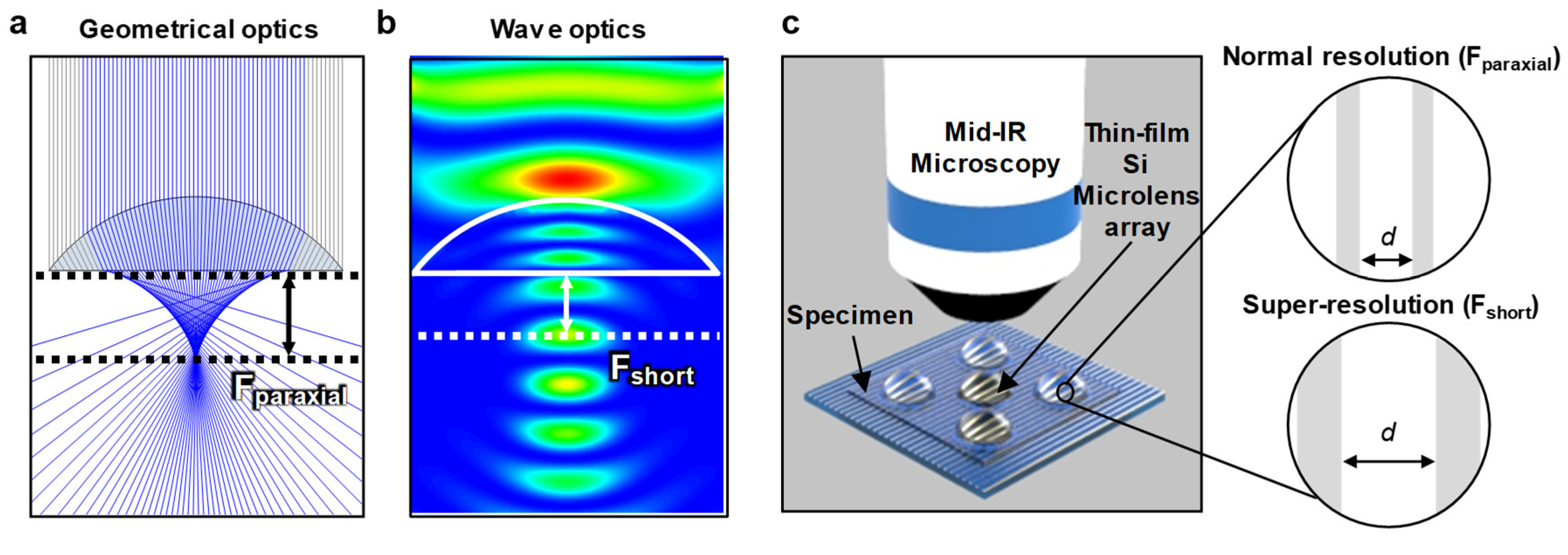
:1. Introduction
2. Materials and Methods
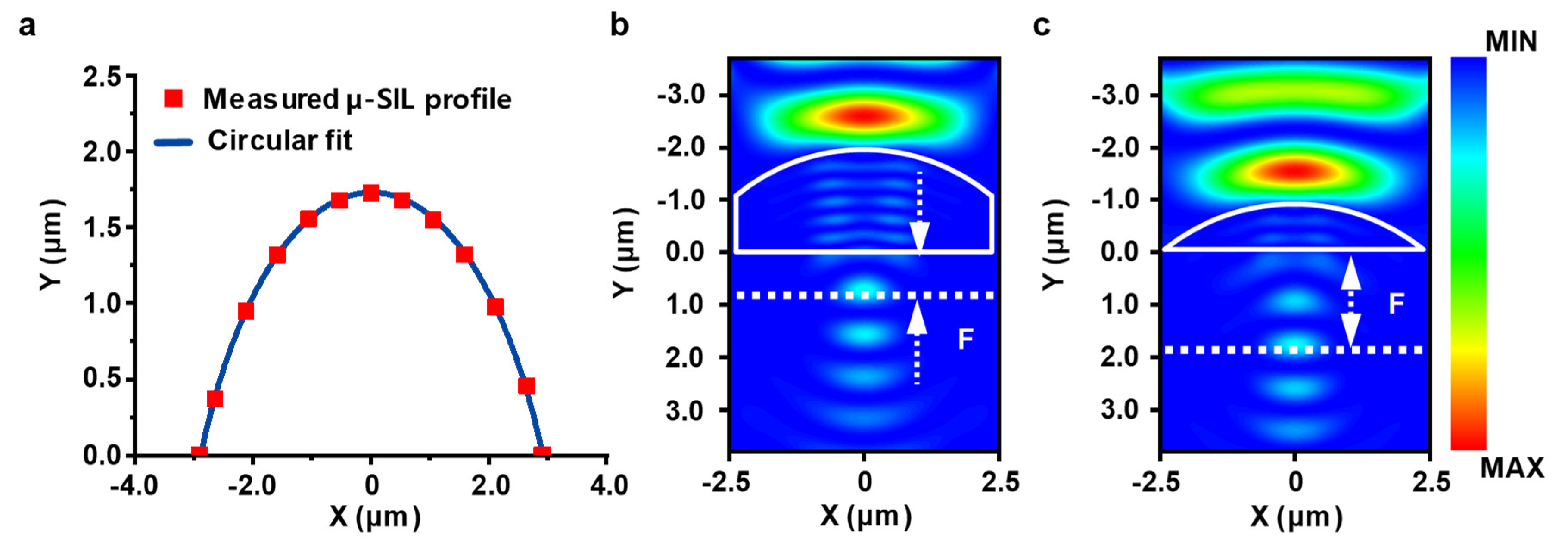
3. Results and Discussion
4. Conclusions
Author Contributions
Funding
Conflicts of Interest
References
- Born, M.; Wolf, E. Principles of Optics, 7th ed.; Cambridge University Press: Cambridge, UK, 2003. [Google Scholar]
- Pendry, J.B. Negative Refraction Makes a Perfect Lens. Phys. Rev. Lett. 2000, 85, 3966. [Google Scholar] [CrossRef] [PubMed]
- Merlin, R. Radiationless Electromagnetic Interference: Evanescent-Field Lenses and Perfect Focusing. Science 2007, 317, 927–929. [Google Scholar] [CrossRef] [PubMed] [Green Version]
- Montgomery, P.; Leong-Hoï, A.; Anstotz, F.; Liu, H.; Simon, B.; Debailleul, M.; Haeberlé, O. Overview of label-free far field optical nanoscopy techniques for nanometrology. Proc. SPIE 2016, 9890, 98900G. [Google Scholar]
- Lee, J.Y.; Hong, B.H.; Kim, W.Y.; Min, S.K.; Kim, Y.K.; Jouravlev, M.V.; Bose, R.; Kim, K.S.; Hwang, I.C.; Kaufman, L.J.; et al. Near-field focusing and magnification through self-assembled nanoscale spherical lenses. Nature 2009, 460, 498–501. [Google Scholar] [CrossRef]
- Wang, Z.; Guo, W.; Li, L.; Luk’yanchuk, B.; Khan, A.; Liu, Z.; Chen, Z.; Hong, M. Optical virtual imaging at 50 nm lateral resolution with a white-light nanoscope. Nat. Commun. 2011, 2, 218. [Google Scholar] [CrossRef] [PubMed] [Green Version]
- Darafsheh, A.; Guardiola, C.; Palovcak, A.; Finlay, J.C.; Cárabe, A. Optical super-resolution imaging by high-index microspheres embedded in elastomers. Opt. Lett. 2015, 40, 5–8. [Google Scholar] [CrossRef] [PubMed]
- Yang, H.; Moullan, N.; Auwerx, J.; Gijs, M.A.M. Super-Resolution Biological Microscopy Using Virtual Imaging by a Microsphere Nanoscope. Small 2014, 10, 1712–1718. [Google Scholar] [CrossRef] [PubMed]
- Allen, K.W.; Farahi, N.; Li, Y.; Limberopoulos, N.I.; Walker, D.E., Jr.; Urbas, A.M.; Liberman, V.; Astratov, V.N. Super-resolution microscopy by movable thin-films with embedded microspheres: Resolution analysis. Ann. Phys. 2015, 527, 513–522. [Google Scholar] [CrossRef] [Green Version]
- Yano, T.; Shibata, S.; Kishi, T. Fabrication of micrometer-size glass solid immersion lens. Appl. Phys. B 2006, 83, 167–170. [Google Scholar] [CrossRef]
- Aboualizadeh, E.; Hirschmugl, C.J. Highlighting IR Spectrochemical Imaging of the Retina. Trends Biochem. Sci. 2018, 43, 650–653. [Google Scholar] [CrossRef]
- Kastyak-Ibrahim, M.Z.; Nasse, M.J.; Rak, C.; Hirschmugl, C.; Del Bigio, M.R.; Albensi, B.C.; Gough, K.M. Biochemical label-free tissue imaging with subcellular-resolution synchrotron FTIR with focal plane array detector. NeuroImage 2012, 60, 376–383. [Google Scholar] [CrossRef] [PubMed]
- Sade, S.; Nagli, L.; Katzir, A. Scanning near field infrared radiometry for thermal imaging of infrared emitters with subwavelength resolution. Appl. Phys. Lett. 2005, 87, 101109. [Google Scholar] [CrossRef]
- Lasch, P.; Naumann, D. Spatial resolution in infrared microspectroscopic imaging of tissues. Biochim. Biophys. Acta 2016, 1758, 814–829. [Google Scholar] [CrossRef] [PubMed] [Green Version]
- Garidel, P.; Boese, M. Mid infrared microspectroscopic mapping and imaging: A bio-analytical tool for spatially and chemically resolved tissue characterization and evaluation of drug permeation within tissue. Microsc. Res. Tech. 2007, 70, 336–349. [Google Scholar] [CrossRef] [PubMed]
- Kim, M.S.; Scharf, T.; Mühlig, S.; Fruhnert, M.; Rockstuhl, C.; Bitterli, R.; Noell, W.; Voelkel, R.; Herzig, H.P. Refraction limit of miniaturized optical systems: A ball-lens example. Opt. Express 2016, 24, 6996–7005. [Google Scholar] [CrossRef] [PubMed] [Green Version]
- Chris, A.M. Mid-infrared imaging with a solid immersion lens and broadband laser source. Appl. Phys. Lett. 2007, 90, 121131. [Google Scholar]
- Ippolito, S.B.; Goldberg, B.B.; Ünlü, M.S. High spatial resolution subsurface microscopy. Appl. Phys. Lett. 2011, 78, 4071. [Google Scholar] [CrossRef] [Green Version]
- Li, Y.; Wolf, E. Three-dimensional intensity distribution near the focus in systems of different Fresnel numbers. J. Opt. Soc. Am. A 1984, 8, 801–808. [Google Scholar] [CrossRef]
- Vokinger, U.; Dändliker, R.; Blattner, P.; Herzig, H.P. Unconventional treatment of focal shift. Opt. Commum. 1998, 157, 218–224. [Google Scholar] [CrossRef] [Green Version]
- Refractive Index Database. Available online: https://refractiveindex.info (accessed on 12 November 2019).
- Nussbaum, P.; Völkel, R.; Herzig, H.P.; Eisner, M.; Haselbeck, S. Design, fabrication and testing of microlens arrays for sensors and microsystems. Pure Appl. Opt. 1997, 6, 617–636. [Google Scholar] [CrossRef] [Green Version]
- Kim, M.S.; Lee, G.J.; Kim, H.M.; Song, Y.M. Parametric Optimization of Lateral NIPIN Phototransistors for Flexible Image Sensors. Sensors 2017, 17, 1774. [Google Scholar] [CrossRef] [PubMed]
- Song, Y.M.; Xie, Y.; Malyarchuk, V.; Xiao, J.; Jung, I.; Choi, K.J.; Liu, Z.; Park, H.; Kim, R.H.; Li, R.; et al. Digital cameras with designs inspired by the Arthropod eye. Nature 2013, 497, 95–99. [Google Scholar] [CrossRef] [PubMed]
- Yang, Y.; Hwang, Y.K.; Cho, H.A.; Song, J.H.; Park, S.J.; Rogers, J.A.; Ko, H.C. Arrays of Silicon Micro/Nanostructures Formed in Suspended Confi gurations for Deterministic Assembly Using Flat and Roller-Type Stamps. Small 2011, 7, 484–491. [Google Scholar] [CrossRef] [PubMed]
- Lin, Z.; Neil, J.N.; Wenchen, Z.; Allen, Y.Y. Fabrication of infrared hexagonal microlens array by novel diamond turning method and precision glass molding. J. Micromech. Microeng. 2019, 29, 065004. [Google Scholar]
- Jovic, A.; Pandraud, G.; Zinoviev, K.; Rubio, J.; Margallo, E. Fabrication process of Si microlenses for OCT systems. Proc. SPIE 2016, 9888, 98880C. [Google Scholar]
- Xiangwei, M.; Feng, C.; Qing, Y.; Hao, B.; Guangqing, D.; Xun, H. Simple fabrication of closed-packed IR microlens arrays on silicon by femtosecond laser wet etching. Appl. Phys. A 2015, 121, 157–162. [Google Scholar]
- Mao, M.; Jiwang, Y. Fabrication of Hexagonal Microlens Arrays on Single-Crystal Silicon Using the Tool-Servo Driven Segment Turning Method. Micromachines 2017, 8, 323. [Google Scholar]
- Xiaojun, Z.; Aiguo, S.; Shuai, W.; Mengjia, W.; Weixing, Y. Fabrication of refractive silicon microlens array with a large focal number and accurate lens profile. Microsyst. Technol. 2019. [Google Scholar] [CrossRef]
- Lei, J.L.; Hang, Z.; Li, M.Z. Fabrication of microlens array on silicon surface using electrochemical wet stamping technique. Appl. Surf. Sci. 2016, 364, 442–445. [Google Scholar] [CrossRef]
- Hao, X.; Zheyao, W. Fabrication of ternary Ge-Se-Sb chalcogenide microlens arrays using thermal reflow. J. Micromech. Microeng. 2019, 29, 085002. [Google Scholar]
- Xue, Q.L.; Lei, Y.; Shuang, N.Y.; Qi, D.C.; Lei, W.; Saulius, J.; Hong, B.S. Optical Nanofabrication of Concave Microlens Arrays. Laser Photonics Rev. 2019, 13, 1800272. [Google Scholar]
- Haijie, Z.; Choi, D.Y.; Xin, G.; Barry, L.D.; Baoping, Z. CMOS compatible fabrication of micro, nano convex silicon lens arrays by conformal chemical vapor deposition. Opt. Express 2017, 25, 3071. [Google Scholar]
- Maslov, A.V.; Astratov, V.N. Imaging of sub-wavelength structures radiating coherently near microspheres. Appl. Phys. Lett. 2016, 108, 051104. [Google Scholar] [CrossRef]


| Materials | Lens Shape | Deformability | Mechanism | Ref. |
|---|---|---|---|---|
| As2+Se3 | Plano-convex | Rigid | Diamond turning and glass molding | [26] |
| Si | Plano-convex | Rigid | Photolithoraphy and dry etching | [27] |
| Si | Plano-concave | Rigid | Fs laser and wet etching | [28] |
| Si | Plano-concave | Rigid | Diamond turning | [29] |
| Si | Plano-convex | Rigid | Photolithoraphy and dry etching | [30] |
| Si | Plano-convex | Rigid | Anodic dissolution process | [31] |
| Ge-Se-Sb chalcogenide | Plano-convex | Rigid | Photolithoraphy and thermal reflow | [32] |
| SiC, GaAs | Plano-concave | Rigid | Fs laser and wet etching | [33] |
| a-Si/H | Plano-convex | Rigid | Micro-fabrication and CVD | [34] |
| Radius (µm) | Diameter (µm) | Height (µm) | Radius to Height Ratio |
|---|---|---|---|
| 3.3 | 5.8 | 1.723 | ~1.9:1 |
© 2020 by the authors. Licensee MDPI, Basel, Switzerland. This article is an open access article distributed under the terms and conditions of the Creative Commons Attribution (CC BY) license (http://creativecommons.org/licenses/by/4.0/).
Share and Cite
Lee, G.J.; Kim, H.M.; Song, Y.M. Design and Fabrication of Microscale, Thin-Film Silicon Solid Immersion Lenses for Mid-Infrared Application. Micromachines 2020, 11, 250. https://doi.org/10.3390/mi11030250
Lee GJ, Kim HM, Song YM. Design and Fabrication of Microscale, Thin-Film Silicon Solid Immersion Lenses for Mid-Infrared Application. Micromachines. 2020; 11(3):250. https://doi.org/10.3390/mi11030250
Chicago/Turabian StyleLee, Gil Ju, Hyun Myung Kim, and Young Min Song. 2020. "Design and Fabrication of Microscale, Thin-Film Silicon Solid Immersion Lenses for Mid-Infrared Application" Micromachines 11, no. 3: 250. https://doi.org/10.3390/mi11030250