Q-Factor Enhancement of Thin-Film Piezoelectric-on-Silicon MEMS Resonator by Phononic Crystal-Reflector Composite Structure

 ,
,  , and
, and
Abstract
:1. Introduction
2. Phononic Crystal Design
3. Resonator Design and Analysis
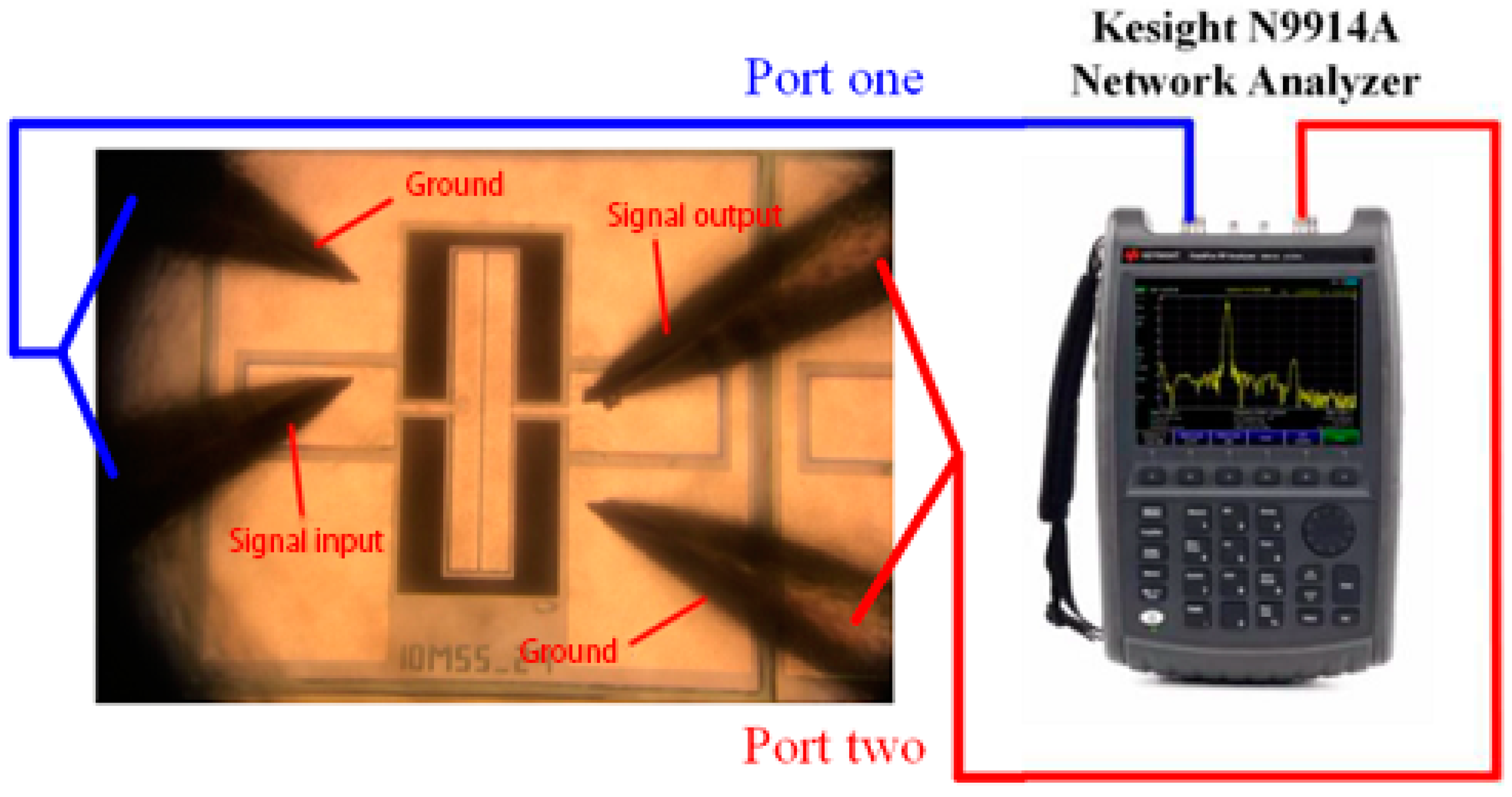
4. Fabrication and Measurement
- Kesight N9914A 4GHz handheld vector network analyzer
- Cascade EPS150RF Video Probe Station
- GGB Picoprobe Model 10 Active Probe Holder
- GGB Model 30-60-W-2-R-125 RF probe
- Calibration chip (used for vector network calibration)
- SMA adapter and coaxial cable
5. Conclusions
Author Contributions
Funding
Conflicts of Interest
References
- Beek, J.T.M.; Puers, R.J. A review of MEMS oscillators for frequency reference and timing applications. J. Micromechanics Microengineering 2011, 22, 013001. [Google Scholar] [CrossRef]
- Tu, C.; Lee, J.E.; Zhang, X.S. Dissipation Analysis Methods and Q-Enhancement Strategies in Piezoelectric MEMS Laterally Vibrating Resonators: A Review. Sensors 2020, 20, 4978. [Google Scholar] [CrossRef] [PubMed]
- Abdolvand, R.; Lavasani, H.M.; Ho, G.K.; Ayazi, F. Thin-film piezoelectric-on-silicon resonators for high-frequency reference oscillator applications. IEEE Trans. Ultrason. Ferroelectr. Freq. Control 2008, 55, 2596–2606. [Google Scholar] [CrossRef] [PubMed]
- Zuo, C.; Sinha, N.; Piazza, G. Very high frequency channel-select MEMS filters based on self-coupled piezoelectric AlN contour-mode resonators. Sens. Actuators A Phys. 2010, 160, 132–140. [Google Scholar] [CrossRef]
- Cassella, C.; Hui, Y.; Qian, Z.; Hummel, G.; Rinaldi, M. Aluminum Nitride Cross-Sectional Lamé Mode Resonators. J. Microelectromechanical Syst. 2016, 25, 275–285. [Google Scholar] [CrossRef]
- Abdolvand, R.; Ayazi, F. Enhanced power handling and quality factor in thin-film piezoelectric-on-substrate resonators. In Proceedings of the IEEE International Ultrasonics Symposium, New York, NY, USA, 28–31 October 2007; pp. 608–611. [Google Scholar]
- Zou, C.; Sinha, N.; Jan, V.D.S.; Piazza, G. Multifrequency pierce oscillators based on piezoelectric AlN contour-mode MEMS technology. J. Microelectromechanical Syst. 2010, 19, 570–580. [Google Scholar]
- Zou, J.; Lin, C.; Pisano, A.P. Anchor loss suppression using butterfly-shaped plates for AlN Lamb wave resonators. In Proceedings of the 2015 Joint Conference of the IEEE International Frequency Control Symposium & the European Frequency and Time Forum, Denver, CO, USA, 12–16 April 2015; pp. 432–435. [Google Scholar] [CrossRef]
- Lee, J.E.-Y.; Yan, J.Z.; Seshia, A.A. Study of lateral mode SOI-MEMS resonators for reduced anchor loss. J. Micromechanics Microengineering 2011, 21, 045010. [Google Scholar] [CrossRef]
- Segovia-Fernandez, J.; Cremonesi, M.; Cassella, C.; Frangi, A.; Piazza, G. Anchor losses in AlN contour mode resonators. J. Microelectromechanical Syst. 2015, 24, 265–275. [Google Scholar] [CrossRef]
- Cassella, C.; Segovia-Fernandez, J.; Piazza, G.; Cremonesi, M.; Frangi, A. Reduction of anchor losses by etched slots in aluminum nitride contour mode resonators. In 2013 Joint European Frequency and Time Forum & International Frequency Control Symposium (EFTF/IFC); IEEE: New York, NY, USA, 2013; pp. 926–929. [Google Scholar] [CrossRef]
- Tu, C.; Lee, J.E.-Y. Enhancing quality factor by etch holes in piezoelectric-on-silicon lateral mode resonators. Sens. Actuators A Phys. 2017, 259, 144–151. [Google Scholar] [CrossRef]
- Zou, J.; Lin, C.-M.; Tang, G.; Pisano, A.P. High-Q butterfly-shaped AlN Lamb wave resonators. IEEE Electron Device Lett. 2017, 38, 1739–1742. [Google Scholar] [CrossRef]
- Zhou, X.; Liu, J.; Bao, F.; Song, Y.; Bao, J.; Zhang, X. Fish Scale-shaped Acoustic Reflector Array for Quality Factor Enhancement of AlN-on-Silicon MEMS Resonator. In 2019 IEEE International Ultrasonics Symposium (IUS); IEEE: New York, NY, USA, 2019; pp. 1720–1723. [Google Scholar] [CrossRef]
- Bao, F.H.; Bao, L.L.; Zhang, X.S.; Zhang, C.; Li, X.Y.; Qin, F.; Zhang, T.; Zhang, Y.; Wu, Z.H.; Jing-Fu, B. Frame structure for thin-film piezoelectric-on-silicon resonator to greatly enhance quality factor and suppress spurious modes. Sens. Actuators A Phys. 2018, 274, 101–108. [Google Scholar] [CrossRef]
- Bao, F.H.; Bao, J.F.; Lee, J.E.Y.; Bao, L.L.; Khan, M.A.; Zhou, X.; Wu, Q.D.; Zhang, T.; Zhang, X.S. Quality factor improvement of piezoelectric MEMS resonator by the conjunction of frame structure and phononic crystals. Sens. Actuators A Phys. 2019, 297, 111541. [Google Scholar] [CrossRef]
- Cowen, A.; Hames, G.; Glukh, K.; Hardy, B. MEMSCAP: PiezoMUMPs Design Handbook. Available online: http://www.memscap.com/_data/assets/pdf_file/0020/5915/PiezoMUMPs.DR.1.3a.pdf (accessed on 1 January 2014).
- Lin, C.-M.; Hsu, J.-C.; Senesky, D.G.; Pisano, A.P. Anchor loss reduction in AlN Lamb wave resonators using phononic crystal strip tethers. In Proceedings of the 2014 IEEE International Frequency Control Symposium (FCS), Taipei, Taiwan, 19–22 May 2014; pp. 371–375. [Google Scholar]
- Abdolvand, R.; Bahreyni, B.; Lee, J.E.Y.; Nabki, F. Micromachined resonators: A review. Micromachines 2016, 7, 160. [Google Scholar] [CrossRef] [PubMed]
- Ho, G.K.; Abdolvand, R.; Sivapurapu, A.; Humad, S.; Ayazi, F. Piezoelectric-on-silicon lateral bulk acoustic wave micromechanical resonators. J. Microelectromechanical Syst. 2008, 17, 512–520. [Google Scholar] [CrossRef]
- Rasouli, M.A.; Bahreyni, B. Independent tuning of frequency and quality factor of microresonators. Appl. Phys. Lett. 2011, 98, 243508. [Google Scholar] [CrossRef]
- Lee, J.E.-Y.; Yan, J.; Seshia, A.A. Low loss HF band SOI wine glass bulk mode capacitive square-plate resonator. J. Micromechanics Microengineering 2009, 19, 074003. [Google Scholar] [CrossRef]
- Prasad, A.; Charmet, J.; Seshia, A.A. Simultaneous interrogation of high-Q modes in a piezoelectric-on-silicon micromechanical resonator. Sens. Actuators A Phys. 2016, 238, 207–214. [Google Scholar] [CrossRef]
- Zhu, H.; Lee, J.E.-Y. Reversed nonlinear oscillations in lamé-mode single-crystal-silicon microresonators. IEEE Electron Device Lett. 2012, 33, 1492–1494. [Google Scholar] [CrossRef]
- Lin, A.T.H.; Yan, J.; Seshia, A.A. Electrostatically transduced face-shear mode silicon MEMS microresonator. In Proceedings of the IEEE International Frequency Control Symposium, Newport Beach, CA, USA, 1–4 June 2010; pp. 534–538. [Google Scholar]
- Luschi, L.; Pieri, F.; Iannaccone, G. A Simple Method for the Design of 1-D MEMS Flexural Phononic Crystals. IEEE Trans. Electron Devices 2016, 63, 4131–4137. [Google Scholar] [CrossRef]
- Harrington, B.P.; Abdolvand, R. In-plane acoustic reflectors for reducing effective anchor loss in lateral-extensional MEMS resonators. J. Micromechanics Microengineering 2011, 21. [Google Scholar] [CrossRef]
- Bao, F.H.; Wu, X.Q.; Zhou, X.; Wu, Q.D.; Zhang, X.S.; Bao, J.F. Spider web-like phononic crystals for piezoelectric MEMS resonators to reduce acoustic energy dissipation. Micromachines 2019, 10, 626. [Google Scholar] [CrossRef] [PubMed] [Green Version]
- Kushwaha, M.S.; Halevi, P.; Dobrzynski, L.; Djafari-Rouhani, B. Acoustic band structure of periodic elastic composites. Phys. Rev. Lett. 1993, 71, 2022–2025. [Google Scholar] [CrossRef] [PubMed]
- Tu, C.; Lee, J.E.Y. VHF-band biconvex AlN-on-silicon micromechanical resonators with enhanced quality factor and suppressed spurious modes. J. Micromechanics Microengineering 2016, 26. [Google Scholar] [CrossRef]
- Binci, L.; Tu, C.; Zhu, H.; Lee, J.E.Y. Planar ring-shaped phononic crystal anchoring boundaries for enhancing the quality factor of Lamb mode resonators. Appl. Phys. Lett. 2016, 109. [Google Scholar] [CrossRef]
- Rawat, U.; Nair, D.R.; DasGupta, A. Piezoelectric-on-silicon array resonators with asymmetric phononic crystal tethering. J. Microelectromechanical Syst. 2017, 26, 773–781. [Google Scholar] [CrossRef]
- Liang, J.; Zhang, H.; Zhang, D.; Duan, X.; Zhang, H.; Pang, W. Design and fabrication of aluminum nitride Lamb wave resonators towards high figure of merit for intermediate frequency filter applications. J. Micromechanics Microengineering 2015, 25. [Google Scholar] [CrossRef]
- Bailie, W.T.; Wu, T.; Bao, J.; Hashimoto, K.-Y. Q-factor enhancement of MEMS resonators with ditetragonal prism shaped phononic crystal (DTP-PnC). In Proceedings of the Symposium on Ultrasonic Electronics, Osaka, Japan, 25–27 November 2020; Volume 41. [Google Scholar]
- Zhu, H.; Lee, J.E.-Y. Design of phononic crystal tethers for frequency selective quality factor enhancement in AlN piezoelectric-on-silicon resonators. Procedia Eng. 2015, 120, 516–519. [Google Scholar] [CrossRef] [Green Version]
- Hopcroft, M.A.; Nix, W.D.; Kenny, T.W. What is the young’s modulus of silicon. J. Microelectromechanical Syst. 2010, 19, 229–238. [Google Scholar] [CrossRef] [Green Version]


| Band Gap Frequency (MHz) | Hole Radius (μm) | Percent Band Gap (%) |
|---|---|---|
| 10.23 | 0.5 | 39.56 |
| 9.48 | 1.0 | 41.23 |
| 9.10 | 1.5 | 40.08 |
| 9.37 | 2.0 | 33.47 |
| 10.34 | 2.5 | 39.26 |
| Parameter Name | Value |
|---|---|
| Young’s modulus (E) | |
| Poisson’s ratio () | |
| Shear modulus (G) | |
| Density () | 2330 kg/m3 |
| N | R | P | P + R | |
|---|---|---|---|---|
| Resonant frequency (), MHz | 10.03 | 10.03 | 10.03 | 10.03 |
| Insertion Loss (IL), dB | −27.01 | −22.79 | −21.64 | −21.59 |
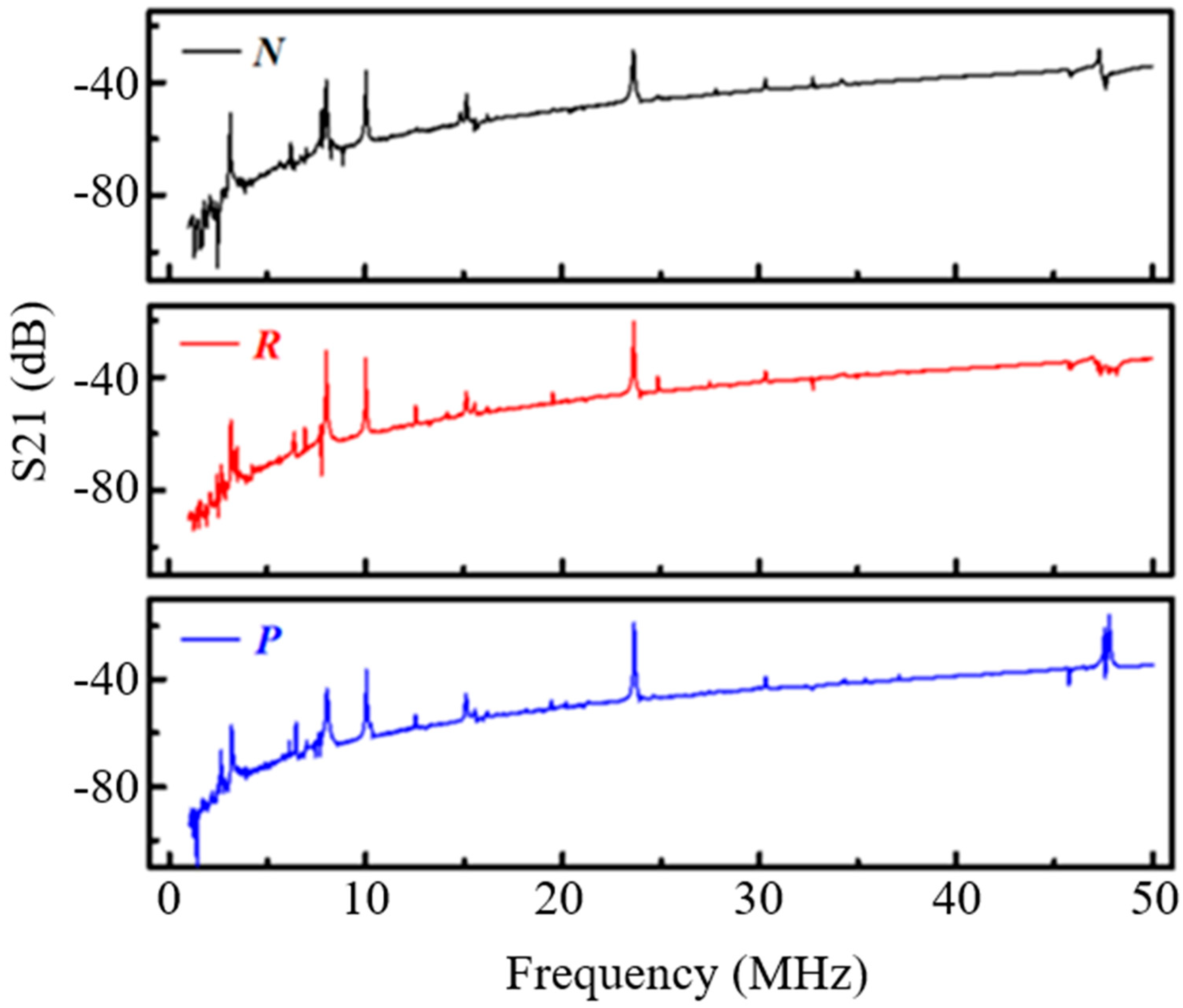
| Loaded Quality factor () | 1570 | 2809 | 4447 | 4682 |
Publisher’s Note: MDPI stays neutral with regard to jurisdictional claims in published maps and institutional affiliations. |
© 2020 by the authors. Licensee MDPI, Basel, Switzerland. This article is an open access article distributed under the terms and conditions of the Creative Commons Attribution (CC BY) license (http://creativecommons.org/licenses/by/4.0/).
Share and Cite
Liu, J.; Workie, T.B.; Wu, T.; Wu, Z.; Gong, K.; Bao, J.; Hashimoto, K.-y. Q-Factor Enhancement of Thin-Film Piezoelectric-on-Silicon MEMS Resonator by Phononic Crystal-Reflector Composite Structure. Micromachines 2020, 11, 1130. https://doi.org/10.3390/mi11121130
Liu J, Workie TB, Wu T, Wu Z, Gong K, Bao J, Hashimoto K-y. Q-Factor Enhancement of Thin-Film Piezoelectric-on-Silicon MEMS Resonator by Phononic Crystal-Reflector Composite Structure. Micromachines. 2020; 11(12):1130. https://doi.org/10.3390/mi11121130
Chicago/Turabian StyleLiu, Jiacheng, Temesgen Bailie Workie, Ting Wu, Zhaohui Wu, Keyuan Gong, Jingfu Bao, and Ken-ya Hashimoto. 2020. "Q-Factor Enhancement of Thin-Film Piezoelectric-on-Silicon MEMS Resonator by Phononic Crystal-Reflector Composite Structure" Micromachines 11, no. 12: 1130. https://doi.org/10.3390/mi11121130