Article

Physical-Based Simulation of the GaN-Based Grooved-Anode Planar Gunn Diode

1
School of Electronic Information, Northwestern Polytechnical University, Xi’an 710072, China
2
The State Key Discipline Laboratory of Wide Band Gap Semiconductor Technology, School of Microelectronics, Xidian University, Xi’an 710071, China
3
School of Electronics and Information Technology, Sun Yat-Sen University, Guangzhou 510275, China
*
Author to whom correspondence should be addressed.
Micromachines 2020, 11(1), 97; https://doi.org/10.3390/mi11010097
Submission received: 7 December 2019 / Revised: 5 January 2020 / Accepted: 9 January 2020 / Published: 16 January 2020
(This article belongs to the Special Issue Wide Bandgap Based Devices: Design, Fabrication and Applications)

Abstract

:
In this paper, a novel gallium nitride (GaN)-based heterostructure Gunn diode is proposed for the first time to enhance the output characteristics of Gunn oscillation waveforms. A well-designed grooved anode contact is adopted to separate the long-channel diode into two short-channel diodes in parallel. If the grooved anode contact is positioned in the middle of the device, the output power nearly doubles in the grooved-anode diode compared with the single-channel ones, as does the output frequency. Based on the numerical results, the best output characteristics are obtained at the 2.0-µm symmetrical grooved-anode diode, which produces nearly 5.48 mW of power at the fundamental frequency of 172.81 GHz, with 3.13% efficiency of power conversion. If the grooved anode contact is not positioned in the middle of the diode, the harmonic frequency would be enhanced. The GaN heterostructure grooved-anode Gunn diode has been demonstrated to be an excellent solid-state source of terahertz oscillator.

1. Introduction

Terahertz (THz) waves (300 GHz–10 THz) have been extensively studied in recent years due to their potential applications in the fields of communication, imaging, radar, spectroscopy and security screening [1,2,3]. Terahertz has been a “research gap” for a long time. Indeed, no powerful radiation sources have been available until the last few years. From a practical point of view, solid-state devices show excellent potential as terahertz sources, which can be integrated with other electronic or optoelectronic devices within a single chip [4]. GaN-based Gunn diodes are one of the most excellent solid-state terahertz oscillators [4] and attract much interest thanks to the unique properties of gallium nitride, such as its wide band gap (3.42 eV) [5], high electron mobility [6], high breakdown field (3.3 MV/cm) [5], high thermal conductivity [7] and so on. In recent years, the research has been mainly concentrated on heterostructural planar Gunn diodes rather than the traditional vertical ones [8,9,10,11,12]. Compared with the traditional vertical Gunn diode, the heterostructural planar Gunn diode has great advantages. First of all, it allows for the easy integration with other devices in terahertz monolithic integrated circuits, as all the contacts of planar diodes are fabricated on one plane [10]. Secondly, its oscillation frequency is controllable by determining the contacts’ distance. Lastly, due to the excellent electron transport properties of the two-dimensional electron gas (2DEG), the planar Gunn diode generates a higher oscillation frequency than bulk ones [9,10,11,12]. However, on one hand, the radio frequency (RF) output power of the planar Gunn diode has been predicted to be much lower than the vertical ones [13,14,15]. On the other hand, the fundamental oscillation of Gunn diodes with a channel length of 1–2 µm reported so far have been far from the terahertz regime [8,9,10,11]. Achieving a Gunn diode with a terahertz oscillation and higher output characteristics is a worldwide problem that should be solved with great urgency. High RF power and high operation frequency seem to be two contradictory pursuits which are difficult to satisfy simultaneously. The shorter the transit region length, the higher the oscillation frequency is [16]. However, the operation bias for short-transit-region diodes is relatively low, which limits their RF output characteristics. In addition, the small-size devices also face a complicated process. Some reported planar Gunn diodes, like nanowire slot diodes and self-switching diodes (SSD) produce very high frequency oscillation, even as high as several THz [17,18,19,20,21]. Nevertheless, all of these emerging devices face the same serious problem–that is, how to generate sufficient RF power. Some theoretical work also shows other solutions, like the harmonic Gunn diode reported in [22,23] and the multi-channel Gunn diode in [24], which either suffers from low RF output power or a complicated process. In order to achieve higher frequency and higher output power simultaneously, for the first time, we propose this new-type grooved-anode Gunn diode, which is realized by simply etching a rectangle groove onto the semiconductor layer at one lithographic step. The anode contact is deposited in the rectangle groove and two cathodes are defined as being adjacent to terminals of AlGaN/GaN heterostructural channel. Therefore, one diode actually turns into two diodes placed in parallel. In the symmetric grooved-anode Gunn diode, where the length of the left and right channel is equal, the output power and oscillation frequency approximately doubles in the grooved-anode diodes compared with the single-channel ones. In the asymmetric grooved-anode Gunn diode, the harmonic frequency is greatly enhanced. In this paper, we present a detailed study into the GaN-based heterostructural grooved-anode Gunn diode based on the Silvaco simulator. We have demonstrated that it effectively improves the RF output power and operation frequency of the Gunn diode simultaneously as compared with many other structures.
The structure of the grooved-anode diode and the simulation method are described in Section 2. The numerical Results and theoretical analysis are given in Section 3. Important conclusions are given in Section 4.

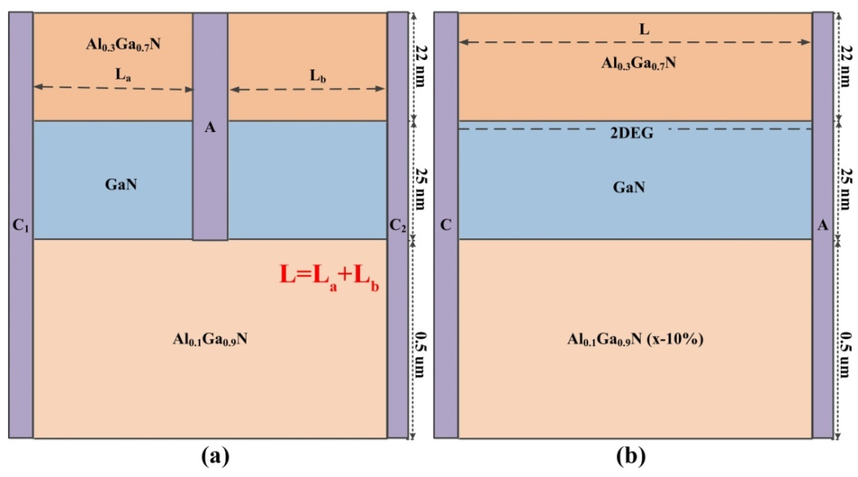
2. Device Structure and Simulation Method

The GaN-based Gunn diode studied in this paper is illustrated in Figure 1. Figure 1a shows the structure of the grooved-anode diode, in which all the structural dimension parameters are labeled clearly. The doping levels of all the material layers are set to be 1 × 1015 cm−3. The adoption of the Al0.1Ga0.9N back barrier layer leads to the enhancing confinement of the 2DEG under a high electric field. A rectangular groove is etched through the GaN layer, which ensures that electrons have individual paths in the left and right channels. To achieve the dual-channel diode, a groove-anode area should be defined, and the groove area is etched using a controllable low-damage chlorine-based Inductively Coupled Plasma- Reactive Ion Etching (ICP-RIE) process [25,26]. The definition of the specific technology parameters should be explored further in the actual manufacturing. The anode ohmic contact is deposited in the rectangle grooves and the two cathode ohmic contacts are defined as vertical contacts instead of surface contacts. On one hand, the vertical contacts introduce the lowest parasitic resistance; on the other hand, electric field peaks are easily formed by the surface contact, which results in the premature breakdown of the devices. The total length of the Gunn diode is set to be L. Meanwhile, in the grooved-anode diode, the length of each channel is set to be La and Lb separately, where La + Lb = L. The width of the device is defined as a default of 1 μm in this 2-D simulator. The vertical ohmic contacts can be realized by Molecular beam epitaxy (MBE) regrown technology. In order to simplify the calculation, we performed the simulations under ideal conditions. We assumed that the groove separates the longer channel completely, and the substrate is totally insulated. Therefore, we do not discuss the coupling effect through the substrate here. An energy balance (EB) model with higher order solution of the general Boltzman transport equation was adopted instead of the drift diffusion (DD) model. The energy relaxation time τε and momentum relaxation time τm for GaN 2DEG are defined as 500 and 4 fs, respectively [27,28,29]. The temperature is set to be 300 K, ideally. In order to calculate the RF output characteristics of the Gunn diode, we use the same method as explained in detail in [22,23,24].
In order to calculate the electrical characteristics of the diode, we put a single-tone sinusoidal voltage of form VDC + VACsin(2πft) across the diode instead of embedding it to a resonant circuit, as the external circuit adds complexity to the calculation and easily results in non-convergence. This method is very popular in the analysis of the RF performance of Gunn diodes [30,31,32,33,34,35,36,37] and its validity has been proved in previous publications [33,34,35,36,37]. The applied DC voltage VDC has to be above a critical value so that the device is biased in the negative differential mobility regime. The DC voltage VDC is proportional to length of the diode and VAC = 1/4VDC. For example, for the 0.6-µm single channel Gunn diode, VDC = 16 V, VAC = 4 V; for the 1.2-µm single-channel diode, VDC = 32 V, VAC = 8 V; for the 0.6-0.6-µm grooved-anode Gunn diode, VDC1 = VDC2 = 16 V, VAC1 = VAC2 = 4 V. The DC-to-AC conversion efficiency η is defined as η = −PAC/PDC (PAC is the time-average AC power; PDC is the dissipated DC power).
The AC power delivered is given by [30]
P AC = V AC T R 0 T R I ( t ) sin ( 2 π ft ) dt
where   T R = 1 f
Similarly, the DC power dissipation in the device is [30]
P DC = V DC T R 0 T R i ( t ) dt

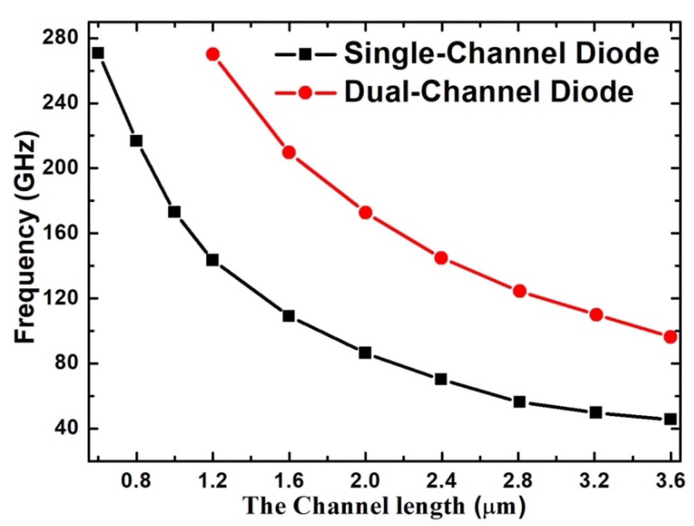
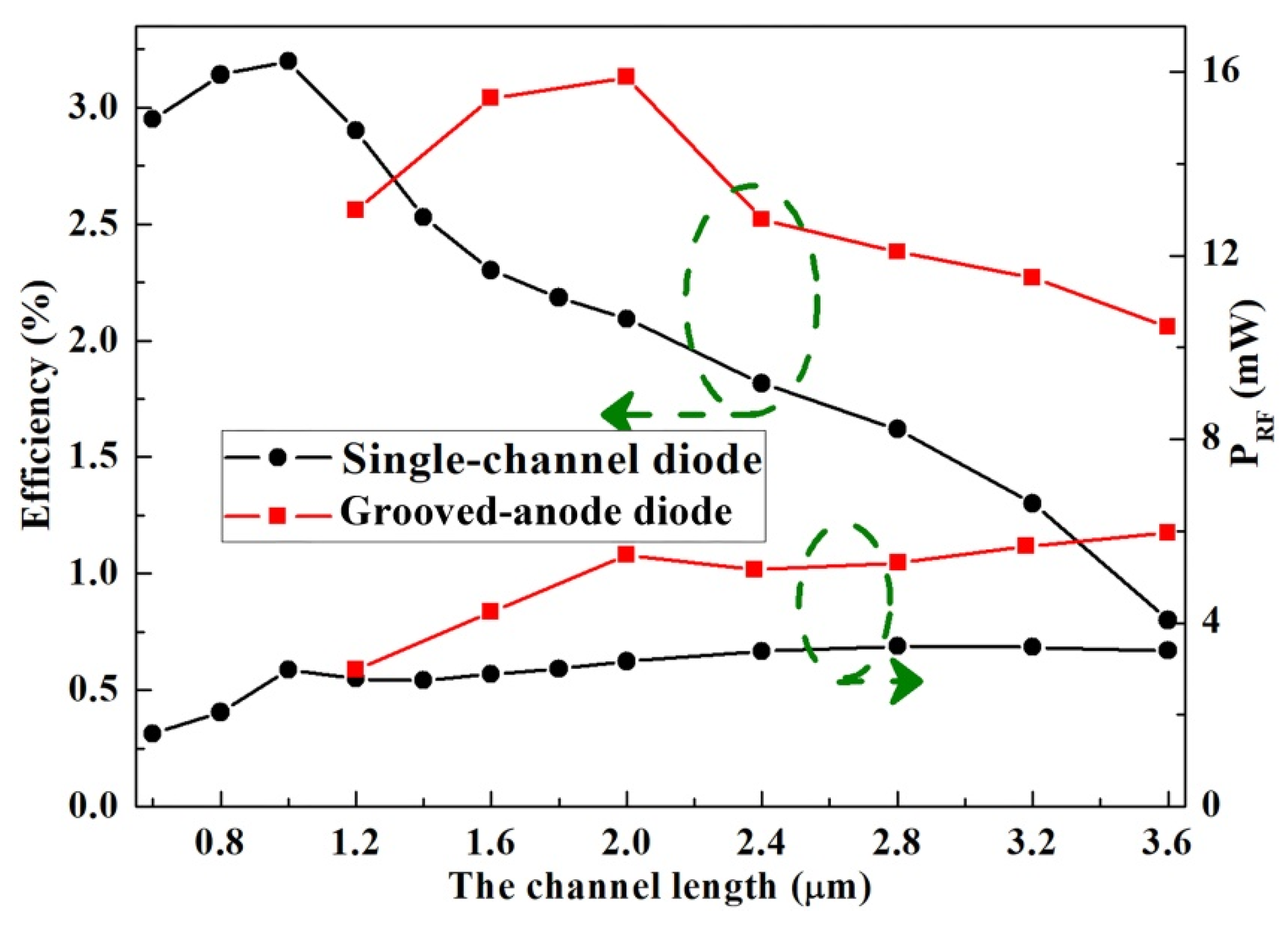
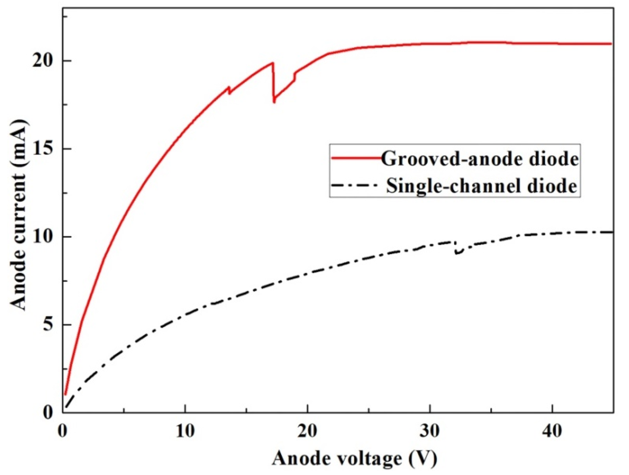
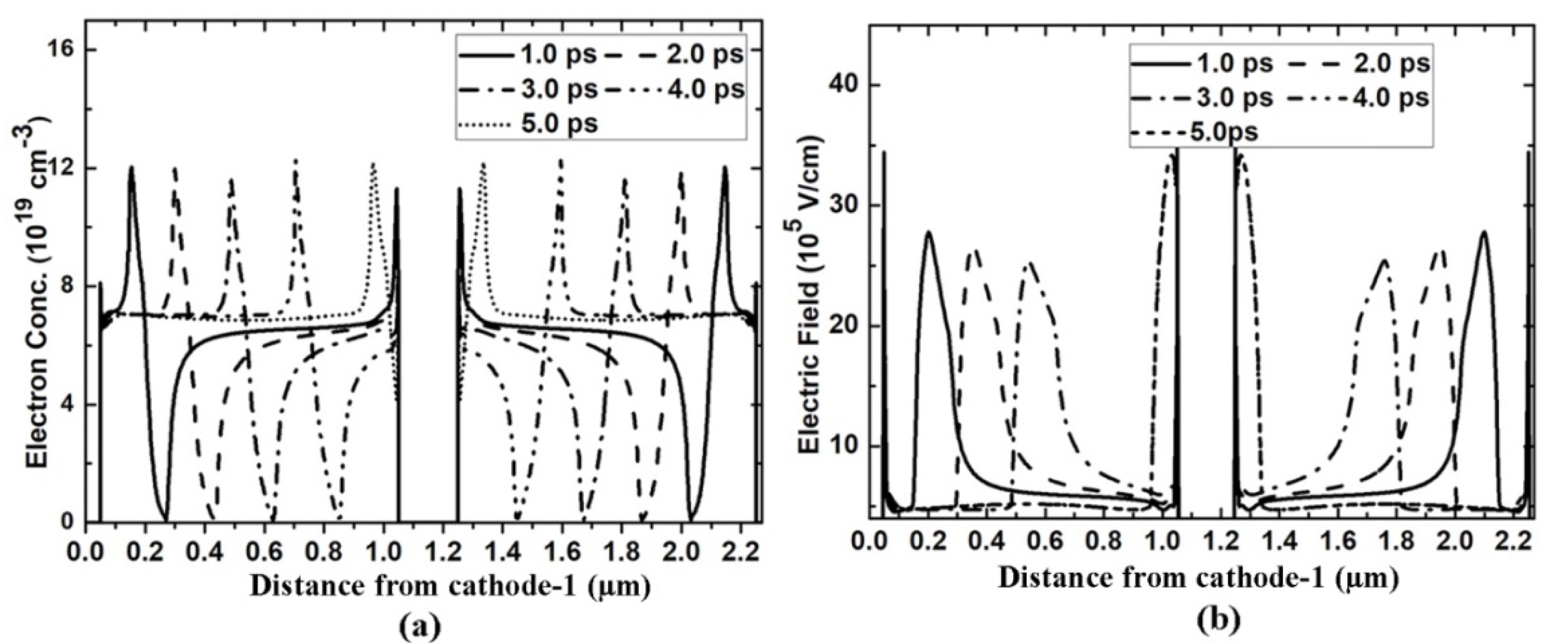
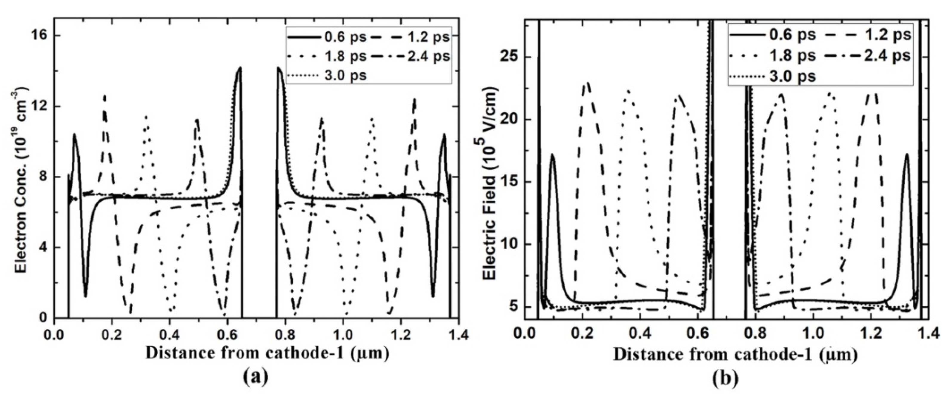
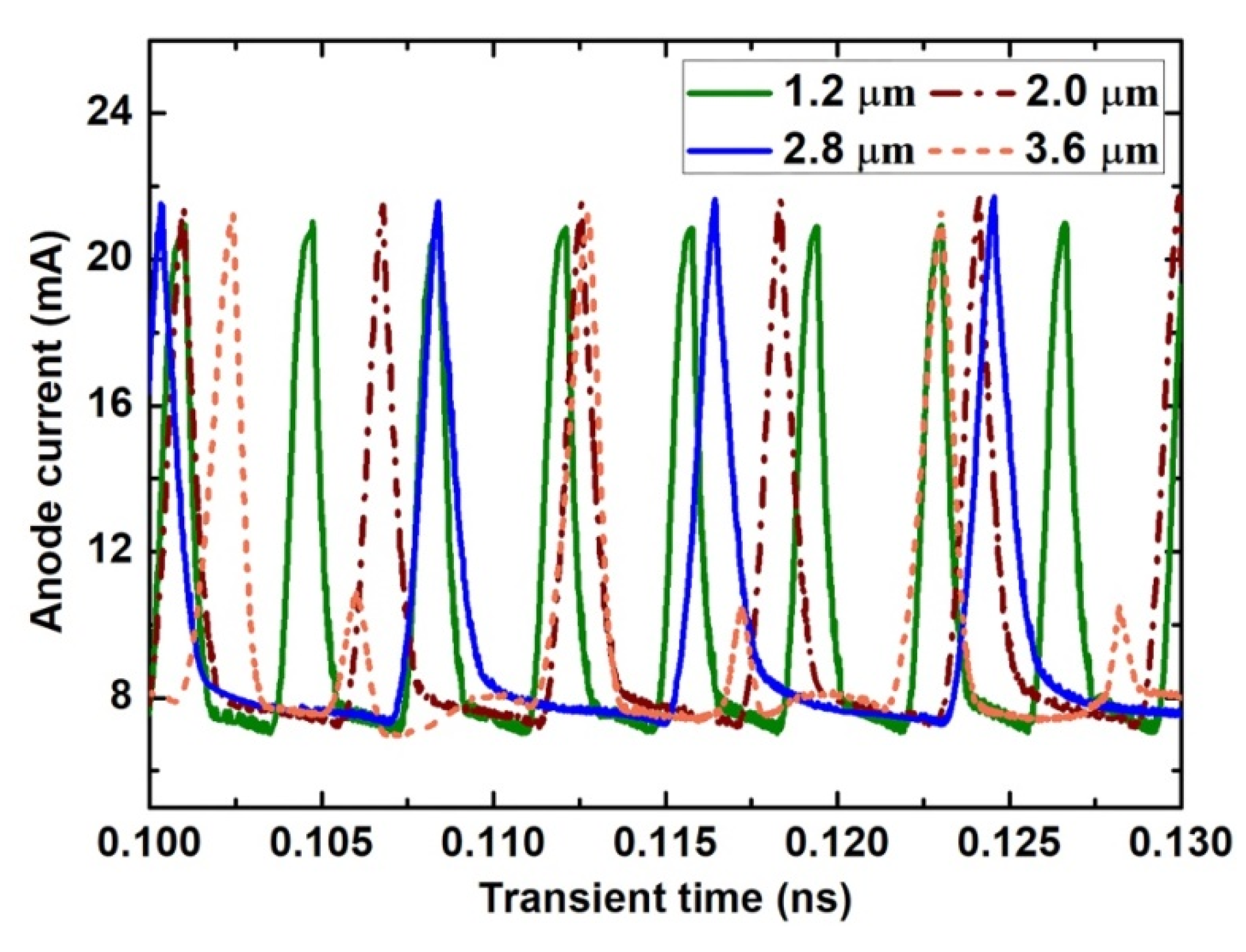
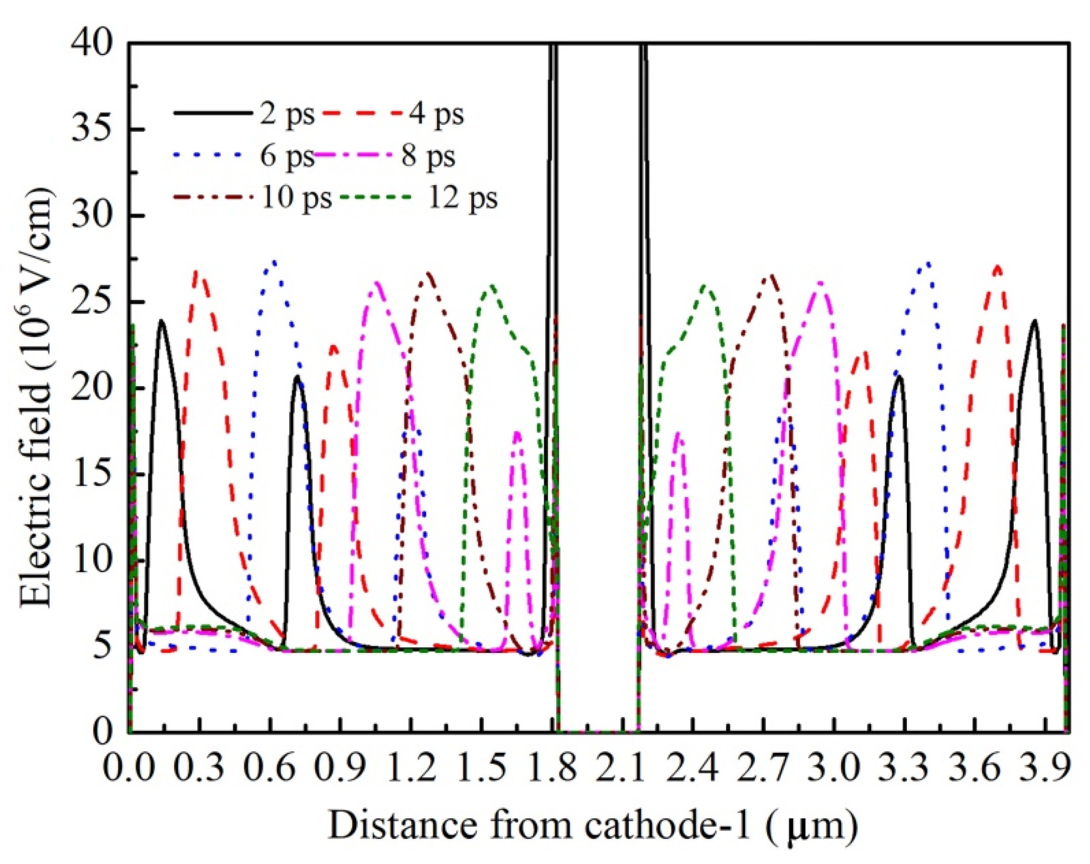
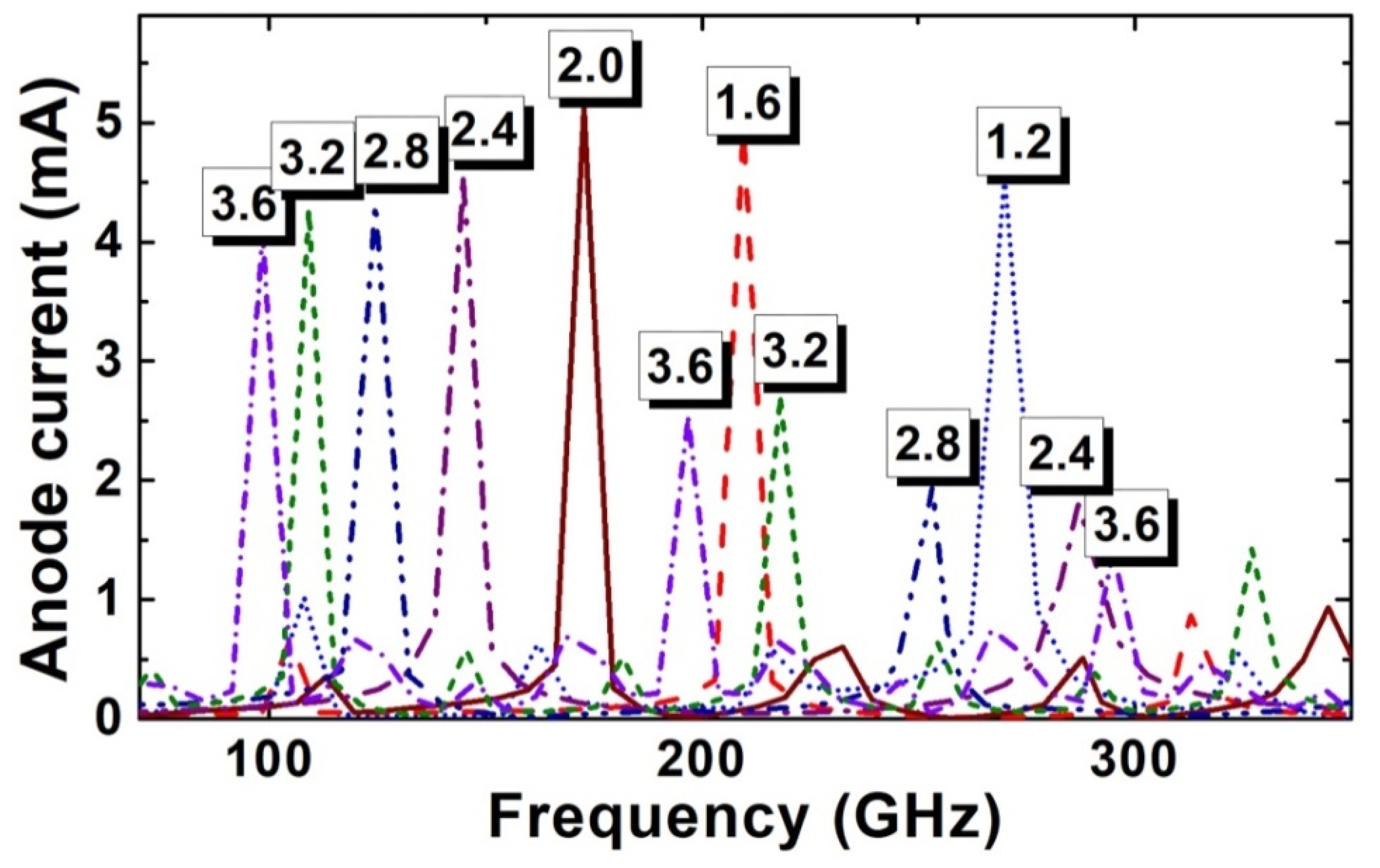
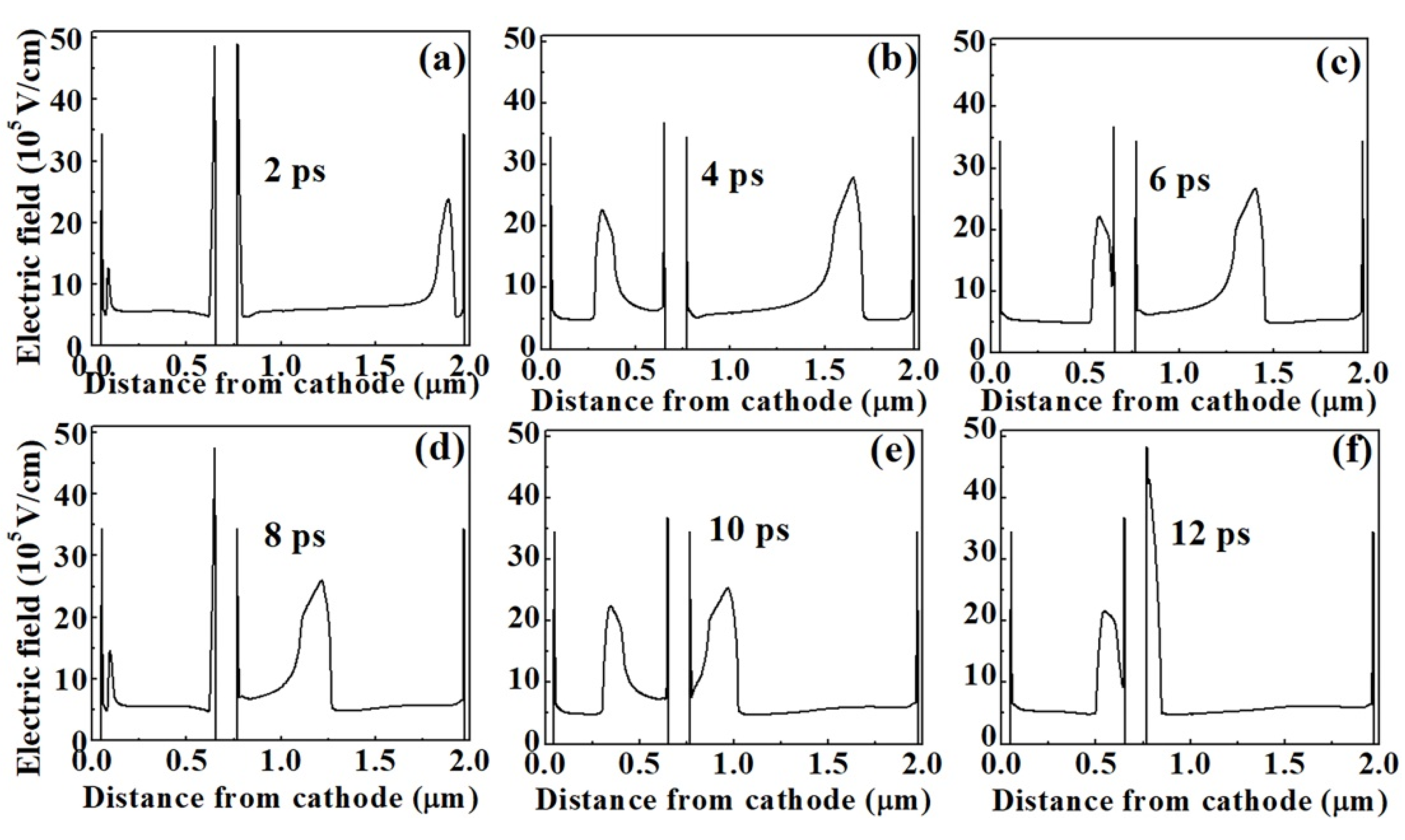
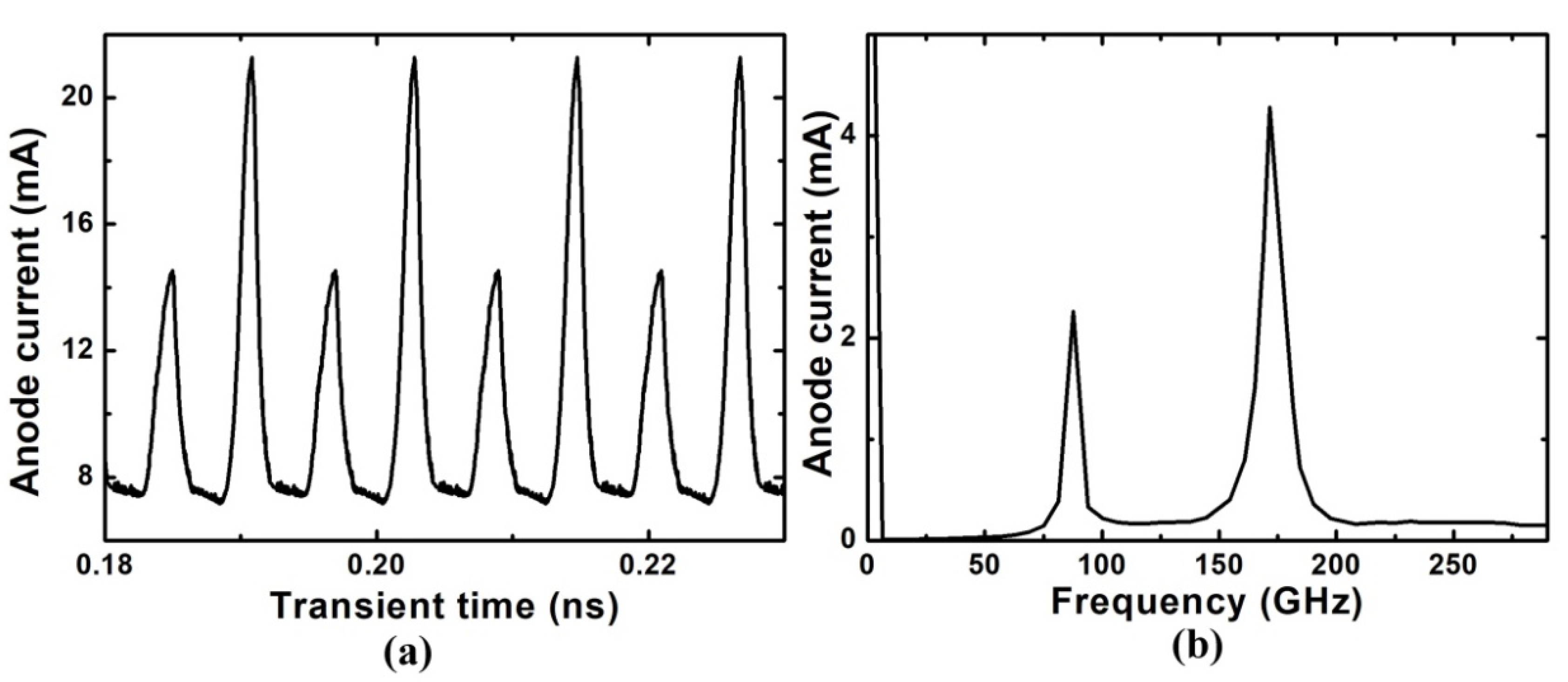
3. Results and Discussion

Both the traditional GaN-based heterostructural Gunn diode with only one channel and the grooved-anode diode were studied as a comparison. In the tradition planar Gunn diode, as the channel length L ranges from 1.2 to 3.6 µm, the frequency f ranges from 143.38 to 45.63 GHz, as shown in Figure 2. The f–L curve of the grooved-anode diode nearly doubles as compared with that of the single-channel diode, as the real channel length of grooved-anode diode is only half of the single-channel diode. The curves also show that f varies inversely to L, which almost matches the formula f = vsat/L. In grooved-anode diode, the best output characteristics are achieved at an L of 2.0 µm. The 2.0-µm-grooved-anode diode operates at a frequency f of 172.81 GHz with a DC-to-AC efficiency η of 3.13% and RF output power PRF of 5.48 mW. Meanwhile, the 2.0-µm-single-channel diode generates a frequency of 86.47 GHz with η of 2.09% and PAC of 3.15 mW, as shown in Figure 2 and Figure 3. Therefore, we conclude that the operating frequency and RF output power nearly doubles as compared with the single-channel diode with the same channel length. In addition, the DC-to-AC efficiency η is also greatly enhanced in the grooved-anode diode.
Figure 4 gives the I-V characteristics for the grooved-anode diode and single-channel diode of 2.0 µm, from which we can see the grooved-anode diode provides practically the same current, twice the value obtained in the single diode. The grooved-anode diode is equal to two shorter diodes in parallel connection, as the grooved anode is designed in the middle of the diode and divides the long channel into two shorter channels; therefore, the anode current doubles. Perturbation occurs in the I-V characteristics as the applied voltage increases above 17 V in the grooved-anode diode and nearly 34 V in the single-channel diode, which means there are electron domains coming into being in the 2DEG channel. When the anode voltage of the 2.0-µm -grooved-anode diodes increases up to 28 V, prefect stable dipole domains come into being. Figure 5a,b separately give the electron concentration profiles and the corresponding electric field profiles during one oscillating period extracted from the 2.0-µm-grooved-anode diode which show the electron periodic movement during one oscillation period. From Figure 5, we can observe the distinct formation of dipole domains rather than accumulation layers. Theoretically, the dipole domain mode is the most stable mode and generates the highest RF output power and efficiency as compared with other operation modes of the Gunn diode. Based on [13], in order to make the GaN Gunn diode work at a stable dipole domain mode, some conditions should be satisfied [16]:
NAC × LAC > 5 × 1013 cm−2
NAC × d > 2 × 1011 cm−2
NAC is the electron concentration of the active channel, LAC is channel length and d is the channel thickness. These conditions are easily satisfied in GaN-based heterostructure Gunn diode, as in the AlGaN/GaN/AlGaN heterojunction, the electron concentration of 2DEG is up to 1019 cm−3. Such a high 2DEG is induced by a strong polarization effect of AlGaN/GaN without any doping and well confined in the quantum well. Therefore, 2DEG is well away from the ionized impurity scattering, ensuring the easier formation of the dipole domain in a short channel length. Even when the length of the GaN planar Gunn diode is reduced to several hundred nanometers or the channel thickness is reduced to several nanometers, the diode can still generate stable dipole-domain mode oscillation, as shown in Figure 6. However, a shorter channel length results in a smaller electron domain. In the 1.2-µm-grooved-anode diode, each channel length is 0.6 µm, which is not long enough for the electron dipole to grow mature before exiting from the anode side. Therefore, comparing Figure 5 and Figure 6, especially the Figure 5b and Figure 6b, from the electric field distribution for the 2.0-µm and 1.2-µm diodes we can conclude that a bigger domain forms in the 2.0-µm-grooved-anode diode. Therefore, higher DC-to-AC efficiency is obtained in the 2.0-µm diode.
Meanwhile, if the channel length is too long, the electron domain grows to its mature size before reaching the anode contact. The remaining channel will be regarded as invalid growth space for the electron domain, which results in the decrease of the efficiency of the Gunn diode. The formation of the electron domain results in the current decline. When the electron domain grows to its full size, the current will drop to its lowest value. If L is too long, the lowest current will last for a period until the electron domain begins to disappear from the anode side. As shown in Figure 7, the lowest-value part of the current wave obviously extends as the channel length L increases, which aggravates the nonlinearity of the oscillation wave, and enhances the harmonic component of the oscillation wave. It is worth noting that two current peaks occur in the 3.6-µm diode, as shown in Figure 7. Figure 8 gives the electron movement tracks in the 3.6-µm diode, which shows that two dipole domains form simultaneously inside each channel; while one forms at near the cathode side, one forms near the middle of the channel. As the electron concentration of 2DEG is very high, therefore, the effective channel lengths for both nucleating points satisfy the condition of the dipole domain. The formation of two domains inside one oscillation circle also aggravates the nonlinearity of the oscillation wave, and weakens the fundamental frequency. In addition, as the two domains restrict each other, neither of them are able to grow to their full size. Therefore, the fundamental and harmonic components of both are reduced. Figure 9 gives the frequency spectrum diagram of the grooved-anode diode for different L from 1.2 to 3.6 µm, which demonstrates that the harmonic component enhances and fundamental component decreases with L. As a result, the noise performance deteriorates with L. In conclusion, in order to avoid the harmonic component enhancement and increase the fundamental component, suitable channel length is of great importance.
We also study the asymmetric grooved-anode Gunn diode, where Lb = 2La = 2.0 µm. In order to ensure that the electric field of each channel is in an appropriate range to generate stable Gunn oscillations, we set VDC2 = 2VDC1 = 53.4 V, VAC2 = 2VAC1 = 13.4 V. As the length of the right channel is twice as long as the length of the left channel, the movement period of the electron domain in the right channel should be twice as long as that in the left channel. This is verified by Figure 10, which shows the electric field profiles in one oscillation period derived in the 1.0-2.0-µm-grooved-anode diode. When the dipole domain in the right channel disappears from the anode contact, the dipole domain in the left channel completes two circles, which results in the two current peaks in the current oscillation wave, as shown in Figure 11a. The small current peak is generated as the domain exits from the shorter channel, and the larger current peak is generated as the domain exits from the longer channel. Therefore, two frequencies are obtained, and the second harmonic frequency is greatly enhanced, as shown in Figure 11b. As the two channels are independent of each other, the fundamental and harmonic frequencies are enhanced at the same time. The frequency of the second harmonic is about 175.47 GHz, η is about 1.85%, and PAC is about 4.45 mW. The asymmetric structure realizes the modulation of the operation frequency via a single diode. By changing the length proportion of the two channels, the size and the number of the harmonic wave are able to be controlled.

4. Conclusions

In this paper, for the first time we propose the grooved-anode planar Gunn diode to greatly enhance the RF output power at a high operation frequency. We present an explicit numerical study into its working principle and output characteristics based on a simulation method. The grooved-anode diode is equal to two shorter diodes in parallel connection, as the grooved anode divides the long channel into two shorter channels. In the symmetric grooved-anode diode, the RF output power is almost doubled in the grooved-anode diode as compared with the single-channel diode. The 1.0-1.0-µm grooved-anode diode shows the best output characteristics. It operates at a fundamental frequency of 172.81 GHz and the corresponding DC-to-AC conversion efficiency is about 3.13%. It produces over 5.48 mW of power, nearly twice as high as that of the 1.0-µm single-channel diode. This novel grooved-anode diode realizes the enhancement of the frequency and RF output power simultaneously, by simply etching a rectangular grooved anode onto the semiconductor layer at one lithographic step, which provides good design ideas in improving the output characteristic of the terahertz sources and other power devices. In the asymmetric 1.0-2.0-µm grooved-anode diode, two frequencies are obtained, and the second harmonic is enhanced as compared with the fundamental wave. The harmonic-enhanced Gunn diode shows its potentials as a mixer or frequency multiplier. Furthermore, it will provide a fast conversion between two different frequencies without connecting with other terahertz oscillators. We have demonstrated that the proposed GaN heterostructure grooved-anode planar Gunn diode is an excellent candidate as a solid-state terahertz device.

Author Contributions

Conceptualization, Y.W. and L.-A.L.; Methodology, J.-P.A.; Software, Y.W.; Validation, Y.W., L.-A.L.; Formal Analysis, Y.W.; Investigation, Y.H.; Resources, J.-P.A.; Data Curation, Y.W.; Writing-Original Draft Preparation, Y.W.; Writing-Review & Editing, L.-A.L.; Visualization, L.-A.L.; Supervision, J.-P.A.; Project Administration, Y.H.; Funding Acquisition, Y.H. All authors have read and agreed to the published version of the manuscript.

Funding

This work was partially supported by the National Key Research and Development Program (Grant No. 2017 YFB043000), the National Natural Science Foundation of China (Grant No. 61274092) and the China Postdoctoral Science Foundation Grant (2019M653554).

Conflicts of Interest

The authors declare no conflict of interest.

References

  1. Rostami, A.; Rasooli, H.; Baghban, H. Terahertz and Infrared Quantum Cascade Lasers. In Terahertz Technology Fundamentals and Applications; Springer: Berlin/Heidelberg, Germany; New York, NY, USA, 2011; Volume 77. [Google Scholar]
  2. Wallance, V.P.; Fitzgerald, A.J.; Shankar, S.; Flanagan, N.; Pye, R.; Cluff, J.; Arnone, D.D. Terahertz pulsed imaging of basal cell carcinoma ex vivo and in vivo. Br. J. Dermatol. 2004, 151, 424–432. [Google Scholar] [CrossRef]
  3. Cohen, I.; Cahan, R.; Shani, G.; Cohen, E.; Abramovich, A. Effect of 99 GHz continuous millimeter wave electro-magnetic radiation on E. coli viability and metabolic activity. Int. J. Radiat. Biol. 2010, 86, 390–399. [Google Scholar] [CrossRef]
  4. Hao, Y.; Yang, L.A.; Zhang, J.C. GaN-based Semiconductor Devices for Terahertz Technology. Terahertz Sci. Technol. 2008, 1, 51–364. [Google Scholar]
  5. Ambacher, O.; Smart, J.; Shealy, J.R.; Weimann, N.G.; Chu, K.; Murphy, M.; Schaff, W.J.; Eastman, L.F.; Dimitrov, R.; Wittmer, L.; et al. Two-dimensional electron gases induced by spontaneous and piezoelectric polarization charges in N- and Ga-face AlGaN/GaN heterostructures. J. Appl. Phys. 1999, 85, 3222–3233. [Google Scholar] [CrossRef] [Green Version]
  6. Piprek, J. Nitride Semiconductors: Principles and Simulation; Wiley: Hoboken, NJ, USA, 2007. [Google Scholar]
  7. Yang, L.A.; Long, S.; Guo, X.; Hao, Y. A comparative investigation on sub-micrometer InN and GaN Gun diodes working at terahertz frequency. J. Appl. Phys. 2012, 111, 104514. [Google Scholar] [CrossRef] [Green Version]
  8. Khalid, A.; Pilgrim, N.J.; Dunn, G.M.; Holland, M.C.; Stanley, C.R.; Thayne, I.G.; Cunmming, D.R.S. A Planar Gunn Diode Operating Above 100 GHz. IEEE Electron Devices Lett. 2007, 28, 849–851. [Google Scholar] [CrossRef]
  9. Pilgrim, N.J.; Khalid, A.; Dunn, G.M.; Cumming, D.R.S. Gunn oscillations in planar heterostructure diodes. Semicond. Sci. Technol. 2008, 23, 075013. [Google Scholar] [CrossRef]
  10. Li, C.; Khalid, A.; Caldwell, S.H.P.; Holland, M.C.; Dunn, G.M.; Thayne, I.G.; Cumming, D.R.S. Design, fabrication and characterization of In0.23Ga0.77As-channel planar Gunn diodes for millimeter wave applications. Solid State Electron. 2011, 64, 67–72. [Google Scholar] [CrossRef]
  11. Song, A.M.; Missous, M.; Omling, P.; Peaker, A.R.; Samuelson, L.; Seifert, W. Operation and high-frequency performance of nanoscale unipolar rectifying diodes. Appl. Phys. Lett. 2003, 83, 1881. [Google Scholar] [CrossRef]
  12. Chowdhury, S.; Mishra, U.K. Lateral and Vertical Transistors Using the AlGaN/GaN Heterostructure. IEEE Trans. Electron Devices 2013, 60, 3060. [Google Scholar] [CrossRef]
  13. Zhang, Y.; Sun, M.; Liu, Z.; Piedra, D.; Pan, M.; Gao, X.; Lin, Y.; Zubair, A.; Yu, L.; Palacios, T. Novel GaN trench MIS barrier Schottky rectifiers with implanted field rings. In Proceedings of the 2016 IEEE International Electron Devices Meeting (IEDM), San Francisco, CA, USA, 3–7 December 2016. [Google Scholar]
  14. Zou, X.; Zhang, X.; Chong, W.C.; Tang, C.W.; Lau, K.M. Vertical LEDs on Rigid and Flexible Substrates Using GaN-on-Si Epilayers and Au-Free Bonding. IEEE Trans. Electron Devices 2016, 63, 1587–1593. [Google Scholar] [CrossRef]
  15. Millithaler, J.F.; Íñiguez-de-la-Torre, I.; Íñiguez-de-la-Torre, A.I.; González, T.; Sangare, P.; Ducournau, G.; Gaquiere, C.; Mateos, J. Optimized V-shape design of GaN nanodiodes for the generation of Gunn oscillations. Appl. Phys. Lett. 2014, 104, 073509. [Google Scholar] [CrossRef] [Green Version]
  16. Sze, S.M.; Ng, K.K. Physics of Semiconductor Devices, 3rd ed.; Wiley: New York, NY, USA, 2007. [Google Scholar]
  17. González, T.; Íñiguez-de-la-Torre, A.; Pardo, D.; Mateos, J.; Song, A.M.J. Monte Carlo analysis of Gunn oscillations in narrow and wide band-gap asymmetric nanodiodes. Phys. Conf. Ser. 2009, 193, 012018. [Google Scholar] [CrossRef]
  18. Xu, K.Y.; Li, J.; Xiong, J.W.; Wang, G. Mutual phase-locking of planar nano-oscillators. AIP Adv. 2014, 4, 067108. [Google Scholar] [CrossRef] [Green Version]
  19. Íñiguez-de-la-Torre, I.; Mateos, J.; González, T.; Sangaré, P.; Faucher, M.; Grimbert, B.; Brandli, V.; Ducournau, G.; Gaquière, C. Searching for THz Gunn oscillations in GaN planar nanodiodes. J. Appl. Phys. 2012, 111, 113705. [Google Scholar] [CrossRef]
  20. Balocco, C.; Halsall, M.; Vinh, N.Q.; Song, A.M. THz operation of asymmetric-nanochannel devices. J. Phys. Condens. Matter 2008, 20, 384203. [Google Scholar] [CrossRef]
  21. Balocco, C.; Kasjoo, S.R.; Lu, X.F.; Zhang, L.Q.; Alimi, Y.; Winnerl, Y.S.; Song, A.M. Room-temperature operation of a unipolar nanodiode at Terahertz frequencies. Appl. Phys. Lett. 2011, 98, 223501. [Google Scholar] [CrossRef] [Green Version]
  22. Wang, Y.; Wang, Z.; Ao, J.; Hao, Y. The modulation of multi-domain and harmonic wave in a GaN planar Gunn diode by recess layer. Semicond. Sci. Technol. 2016, 31, 025001. [Google Scholar] [CrossRef]
  23. Wang, Y.; Yang, L.; Wang, Z. Ultra-short channel GaN high electron mobility transistor-like Gunn diode with composite contact. J. Appl. Phys. 2014, 116, 849. [Google Scholar] [CrossRef]
  24. Wang, Y.; Yang, L.; Wang, Z. The enhancement of the output characteristics in the GaN based multiple-channel planar Gunn diode. Phys. Status Solidi 2016, 213, 1252–1258. [Google Scholar] [CrossRef]
  25. Lanford, W.B.; Tanaka, T.; Otoki, Y.; Adesida, I. Recessed-gate enhancement-mode GaN HEMT with high threshold voltage. Electron. Lett. 2015, 41, 449–450. [Google Scholar] [CrossRef]
  26. Wang, H.; Wang, Y.; Zhu, G.; Wang, Q.; Xin, Q.; Han, L.; Song, A. A novel thermally evaporated etching mask for low-damage dry etching. IEEE Trans. Nanotechnol. 2017, 16, 290–295. [Google Scholar] [CrossRef] [Green Version]
  27. Balkan, N.; Arikan, M.C.; Gokden, S.; Tilak, V.; Schaff, B.; Shealy, R.J. Energy and momentum relaxation of hot electrons in GaN/AlGaN. J. Phys. Condens. Matter 2002, 14, 3457. [Google Scholar] [CrossRef]
  28. Matulionis, A.; Liberis, J. Microwave noise in AlGaN/GaN channels. IEE Proc. Circuits Devices Syst. 2004, 151, 148–154. [Google Scholar] [CrossRef]
  29. Matulionis, A.; Morkoç, H. Hot phonons in InAlN/AlN/GaN heterostructure 2DEG channels. In Proceedings of the SPIE OPTO: Integrated Optoelectronic Devices, San Jose, CA, USA, 18 February 2009. [Google Scholar]
  30. Dunn, G.; Kearney, M.J. A theoretical study of differing active region doping profiles for W-band (75–110 GHz) InP Gunn diodes. Semicond. Sci. Technol. 2003, 18, 794. [Google Scholar] [CrossRef]
  31. Sevik, C.; Bulutay, C. Gunn oscillations in GaN channels. Semicond. Sci. Technol. 2004, 19, 190. [Google Scholar] [CrossRef]
  32. Tech, Y.P.; Dunn, G.M.; Priestley, N.; Carr, M. Monte Carlo simulations of asymmetry multiple transit region Gunn diodes. Semicond. Sci. Technol. 2005, 20, 418. [Google Scholar]
  33. García, S.; Vasallo, B.G.; Mateos, J.; González, T. Time-domain Monte Carlo simulations of resonant-circuit operation of GaN Gunn diodes. In Proceedings of the 9th Spanish Conference on Electronic Devices (CDE 2013), Valladolid, Spain, 12–14 February 2013; pp. 79–82. [Google Scholar]
  34. Kamoua, R.; Eisle, H.; Haddad, G.I. D-band (110–170 GHz), InP gunn devices. Solide State Electron. 1993, 36, 1547. [Google Scholar]
  35. Judaschke, R. Comparison of modulated impurity-concentration inp transferred electron devices for power generation at frequencies above 130 GHz. IEEE Trans. Microw. Theory Tech. 2000, 48, 719–724. [Google Scholar] [CrossRef]
  36. Zybura, M.F.; Jones, S.H.; Tait, G.; Duva, J.M. Efficient computer aided design of GaAs and InP millimeter wave transferred electron devices including detailed thermal analysis. Solid State Electron. 1995, 38, 873–880. [Google Scholar] [CrossRef]
  37. García, S.; Íñiguez-de-la-Torre, I.; Pérez, S.; Mateos, J.; González, T. Numerical study of sub-millimeter Gunn oscillations in InP and GaN vertical diodes: Dependence on bias, doping, and length. J. Appl. Phys. 2013, 114, 074503. [Google Scholar] [CrossRef]
Figure 1. Schematic structures of GaN-based heterostructure Gunn diodes: (a) Grooved-anode diode, (b) Single-channel diode.
Micromachines 11 00097 g001
Figure 2. Variation of frequency f with the channel length L in the grooved-anode diode and single-channel diode.
Micromachines 11 00097 g002
Figure 3. Variation of efficiency η with the channel length L and RF output power PAC with L in the grooved-anode diode and the variation of the single-channel diode.
Micromachines 11 00097 g003
Figure 4. DC I-V output for the grooved-anode diode and single-channel diode as L = 2.0 µm.
Micromachines 11 00097 g004
Figure 5. (a) Electron concentration and (b) Electric field profiles in one oscillation period in the grooved-anode diode as L = 2.0 µm.
Micromachines 11 00097 g005
Figure 6. (a) Electron concentration and (b) Electric field profiles in one oscillation period in the grooved-anode diode as L = 1.2 µm.
Micromachines 11 00097 g006
Figure 7. The current oscillation wave in the symmetric grooved-anode diode.
Micromachines 11 00097 g007
Figure 8. The electric field profiles in one oscillation period in the grooved-anode diode as L = 1.8 µm.
Micromachines 11 00097 g008
Figure 9. The frequency spectrum diagram of the grooved-anode diode for different L.
Micromachines 11 00097 g009
Figure 10. (af) The electric field profiles derived at the same time step in one oscillation period in the grooved-anode diode as La = 1.0 µm and Lb = 2.0 µm.
Micromachines 11 00097 g010
Figure 11. (a) The current oscillation wave and (b) the frequency spectrum diagram of the grooved-anode diode, where La = 1.0 µm and Lb = 2.0 µm.
Micromachines 11 00097 g011

