A MEMS-Based Quad-Wavelength Hybrid Plasmonic–Pyroelectric Infrared Detector

 , ,
, , 
Abstract
:1. Introduction
2. Design and Fabrication
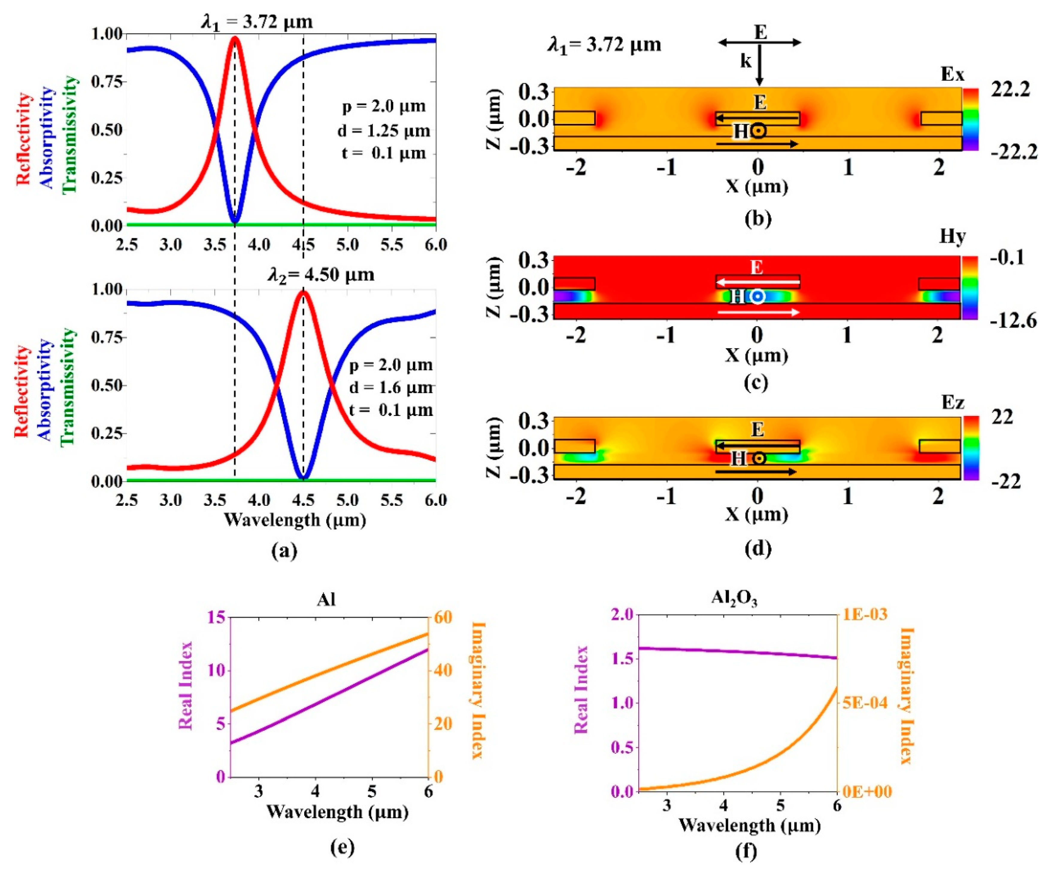
2.1. Structure Design
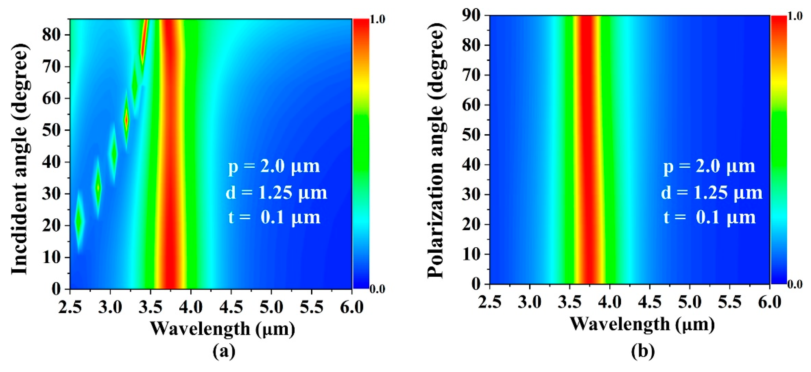
2.2. Simulation
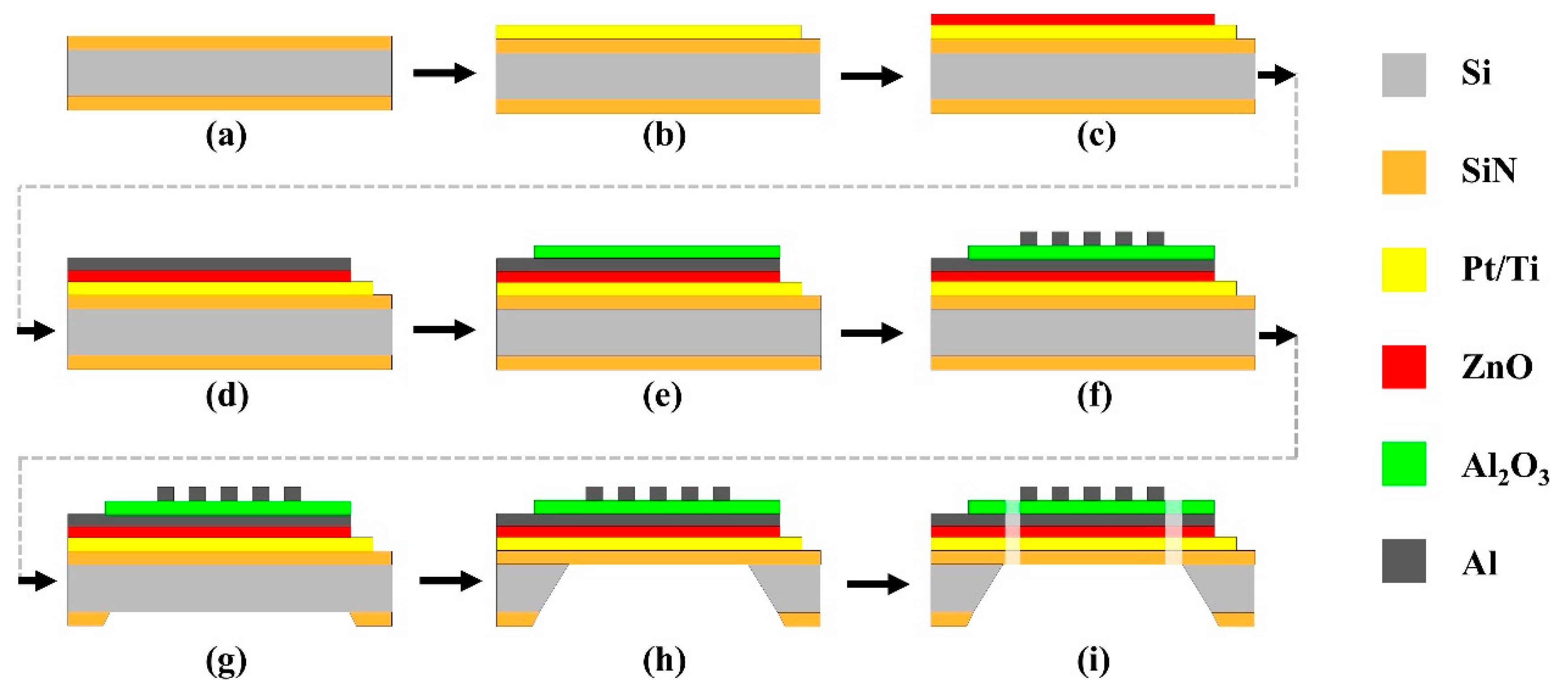
2.3. Fabrication
3. Results and Discussion
4. Conclusions
Author Contributions
Funding
Acknowledgments
Conflicts of Interest
References
- Ng, D.; Fralick, G. Use of a multiwavelength pyrometer in several elevated temperature aerospace applications. Rev. Sci. Instrum. 2001, 72, 1522–1530. [Google Scholar] [CrossRef]
- Felice, R.A. The Spectropyrometer—A Practical Multi-wavelength Pyrometer. AIP Conf. Proc. 2003, 684, 711–716. [Google Scholar]
- Boebel, F.G.; Möller, H.; Hertel, B.; Grothe, H.; Schraud, G.; Schröder, S.; Chow, P. In situ film thickness and temperature control of molecular beam epitaxy growth by pyrometric interferometry. J. Cryst. Growth 1995, 150, 54–61. [Google Scholar] [CrossRef]
- Fu, T.; Liu, J.; Duan, M.; Zong, A. Temperature measurements using multicolor pyrometry in thermal radiation heating environments. Rev. Sci. Instrum. 2014, 85, 044901. [Google Scholar] [CrossRef] [Green Version]
- Boboridis, K.; Obst, A.W. A High-Speed Four-Channel Infrared Pyrometer. AIP Conf. Proc. 2003, 684, 759–764. [Google Scholar] [Green Version]
- Dinh, T.-V.; Choi, I.-Y.; Son, Y.-S.; Kim, J.-C. A review on non-dispersive infrared gas sensors: Improvement of sensor detection limit and interference correction. Sens. Actuators B Chem. 2016, 231, 529–538. [Google Scholar] [CrossRef]
- Hodgkinson, J.; Smith, R.; Ho, W.O.; Saffell, J.R.; Tatam, R.P. Non-dispersive infra-red (NDIR) measurement of carbon dioxide at 4.2 μm in a compact and optically efficient sensor. Sens. Actuators B Chem. 2013, 186, 580–588. [Google Scholar] [CrossRef]
- Hasan, D.; Lee, C.; Hasan, D.; Lee, C. Hybrid Metamaterial Absorber Platform for Sensing of CO2 Gas at Mid-IR. Adv. Sci. 2018, 5, 1700581. [Google Scholar] [CrossRef]
- Hodgkinson, J.; Tatam, R.P. Optical gas sensing: A review. Meas. Sci. Technol. 2013, 24, 012004. [Google Scholar] [CrossRef]
- Tan, Q.; Zhang, W.; Xue, C.; Xiong, J.; Ma, Y.; Wen, F. Design of mini-multi-gas monitoring system based on IR absorption. Opt. Laser Technol. 2008, 40, 703–710. [Google Scholar] [CrossRef]
- Wang, L.; Mizaikoff, B. Application of multivariate data-analysis techniques to biomedical diagnostics based on mid-infrared spectroscopy. Anal. Bioanal. Chem. 2008, 391, 1641–1654. [Google Scholar] [CrossRef]
- Elliott, A.; Ambrose, E.J. Structure of Synthetic Polypeptides. Nature 1950, 165, 921–922. [Google Scholar] [CrossRef]
- López-Lorente, Á.I.; Mizaikoff, B. Mid-infrared spectroscopy for protein analysis: Potential and challenges. Anal. Bioanal. Chem. 2016, 408, 2875–2889. [Google Scholar] [CrossRef]
- Moore, D.J.; Sills, R.H.; Mendelsohn, R. Peroxidation of erythrocytes: FTIR spectroscopy studies of extracted lipids, isolated membranes, and intact cells. Biospectroscopy 1995, 1, 133–140. [Google Scholar] [CrossRef]
- Wolkers, W.F.; Hoekstra, F.A. In situ FTIR Assessment of Desiccation-Tolerant Tissues. Spectroscopy 2003, 17, 297–313. [Google Scholar] [CrossRef]
- Volkov, V.V.; Chelli, R.; Righini, R. Domain Formation in Lipid Bilayers Probed by Two-Dimensional Infrared Spectroscopy. J. Phys. Chem. B 2006, 110, 1499–1501. [Google Scholar] [CrossRef]
- Marks, R.S.; Abdulhalim, I. Nanomaterials for Water Management: Signal Amplification for Biosensing from Nanostructures; Pan Stanford: New York, NY, USA, 2015; ISBN 9789814463478. [Google Scholar]
- Nagao, T.; Han, G.; Hoang, C.; Wi, J.-S.; Pucci, A.; Weber, D.; Neubrech, F.; Silkin, V.M.; Enders, D.; Saito, O.; et al. Plasmons in nanoscale and atomic-scale systems. Sci. Technol. Adv. Mater. 2010, 11, 054506. [Google Scholar] [CrossRef]
- Ariyawansa, G.; Rinzan, M.B.M.; Alevli, M.; Strassburg, M.; Dietz, N.; Perera, A.G.U.; Matsik, S.G.; Asghar, A.; Ferguson, I.T.; Luo, H.; et al. GaN/AlGaN ultraviolet/infrared dual-band detector. Appl. Phys. Lett. 2006, 89, 091113. [Google Scholar] [CrossRef]
- Hudson, M.K.; Busch, K.W. Infrared emission from a flame as the basis for chromatographic detection of organic compounds. Anal. Chem. 1987, 59, 2603–2609. [Google Scholar] [CrossRef]
- Liu, Z.; Kim, A.K. Review of Recent Developments in Fire Detection Technologies. J. Fire Prot. Eng. 2003, 13, 129–151. [Google Scholar] [CrossRef] [Green Version]
- Romero, C.; Li, X.; Keyvan, S.; Rossow, R. Spectrometer-based combustion monitoring for flame stoichiometry and temperature control. Appl. Therm. Eng. 2005, 25, 659–676. [Google Scholar] [CrossRef]
- Berni, J.; Zarco-Tejada, P.J.; Suarez, L.; Fereres, E. Thermal and Narrowband Multispectral Remote Sensing for Vegetation Monitoring From an Unmanned Aerial Vehicle. IEEE Trans. Geosci. Remote Sens. 2009, 47, 722–738. [Google Scholar] [CrossRef] [Green Version]
- Meriaudeau, F. Real time multispectral high temperature measurement: Application to control in the industry. Image Vis. Comput. 2007, 25, 1124–1133. [Google Scholar] [CrossRef]
- Gowen, A.A.; Tiwari, B.K.; Cullen, P.J.; McDonnell, K.; O’Donnell, C.P. Applications of thermal imaging in food quality and safety assessment. Trends Food Sci. Technol. 2010, 21, 190–200. [Google Scholar] [CrossRef]
- Ünlü, M.S.; Strite, S. Resonant cavity enhanced photonic devices. J. Appl. Phys. 1995, 78, 607–639. [Google Scholar] [CrossRef]
- Emsley, M.K.; Dosunmu, O.; Unlu, M.S. High-speed resonant-cavity-enhanced silicon photodetectors on reflecting silicon-on-insulator substrates. IEEE Photonics Technol. Lett. 2002, 14, 519–521. [Google Scholar] [CrossRef]
- Boeberl, M.; Fromherz, T.; Schwarzl, T.; Springholz, G.; Heiss, W. IV-VI resonant-cavity enhanced photodetectors for the mid-infrared. Semicond. Sci. Technol. 2004, 19, L115–L117. [Google Scholar] [CrossRef]
- Arnold, M.; Zimin, D.; Zogg, H. Resonant-cavity-enhanced photodetectors for the mid-infrared. Appl. Phys. Lett. 2005, 87, 141103. [Google Scholar] [CrossRef]
- Wehner, J.G.A.; Musca, C.A.; Sewell, R.H.; Dell, J.M.; Faraone, L. Mercury cadmium telluride resonant-cavity-enhanced photoconductive infrared detectors. Appl. Phys. Lett. 2005, 87, 211104. [Google Scholar] [CrossRef]
- Kishino, K.; Unlu, M.S.; Chyi, J.-I.; Reed, J.; Arsenault, L.; Morkoc, H. Resonant cavity-enhanced (RCE) photodetectors. IEEE J. Quantum Electron. 1991, 27, 2025–2034. [Google Scholar] [CrossRef]
- Landy, N.I.; Sajuyigbe, S.; Mock, J.J.; Smith, D.R.; Padilla, W.J. Perfect Metamaterial Absorber. Phys. Rev. Lett. 2008, 100, 207402. [Google Scholar] [CrossRef] [PubMed]
- Watts, C.M.; Liu, X.; Padilla, W.J. Metamaterial Electromagnetic Wave Absorbers. Adv. Mater. 2012, 24, OP98–OP120. [Google Scholar] [CrossRef] [PubMed]
- Dao, T.D.; Ishii, S.; Yokoyama, T.; Sawada, T.; Sugavaneshwar, R.P.; Chen, K.; Wada, Y.; Nabatame, T.; Nagao, T. Hole Array Perfect Absorbers for Spectrally Selective Midwavelength Infrared Pyroelectric Detectors. ACS Photonics 2016, 3, 1271–1278. [Google Scholar] [CrossRef]
- Liu, X.; Tyler, T.; Starr, T.; Starr, A.F.; Jokerst, N.M.; Padilla, W.J. Taming the Blackbody with Infrared Metamaterials as Selective Thermal Emitters. Phys. Rev. Lett. 2011, 107, 045901. [Google Scholar] [CrossRef] [PubMed] [Green Version]
- Hao, J.; Wang, J.; Liu, X.; Padilla, W.J.; Zhou, L.; Qiu, M. High performance optical absorber based on a plasmonic metamaterial. Appl. Phys. Lett. 2010, 96, 251104. [Google Scholar] [CrossRef]
- Korotchenkov, G.S. Handbook of Gas Sensor Materials: Properties, Advantages and Shortcomings for Applications. New Trends and Technologies; Springer: Berlin, Germany, 2013. [Google Scholar]
- Esler, M.B.; Griffith, D.W.; Wilson, S.R.; Steele, L.P. Precision trace gas analysis by FT-IR spectroscopy. 1. Simultaneous analysis of CO2, CH4, N2O, and CO in air. Anal. Chem. 2000, 72, 206–215. [Google Scholar] [CrossRef] [PubMed]
- Dao, T.D.; Chen, K.; Ishii, S.; Ohi, A.; Nabatame, T.; Kitajima, M.; Nagao, T. Infrared Perfect Absorbers Fabricated by Colloidal Mask Etching of Al-Al2O3-Al Trilayers. ACS Photonics 2015, 2, 964–970. [Google Scholar] [CrossRef]
- Synopsys’s Rsoft. Available online: https://www.synopsys.com (accessed on 7 April 2019).
- Malka, D.; Danan, Y.; Ramon, Y.; Zalevsky, Z.; Malka, D.; Danan, Y.; Ramon, Y.; Zalevsky, Z. A Photonic 1 × 4 Power Splitter Based on Multimode Interference in Silicon–Gallium-Nitride Slot Waveguide Structures. Materials 2016, 9, 516. [Google Scholar] [CrossRef]
- Shoresh, T.; Katanov, N.; Malka, D. 1 × 4 MMI visible light wavelength demultiplexer based on a GaN slot-waveguide structure. Photonics Nanostruct. Fundam. Appl. 2018, 30, 45–49. [Google Scholar] [CrossRef]
- Yokoyama, T.; Dao, T.D.; Chen, K.; Ishii, S.; Sugavaneshwar, R.P.; Kitajima, M.; Nagao, T. Spectrally Selective Mid-Infrared Thermal Emission from Molybdenum Plasmonic Metamaterial Operated up to 1000 °C. Adv. Opt. Mater. 2016, 4, 1987–1992. [Google Scholar] [CrossRef]
- Khorasaninejad, M.; Zhu, A.Y.; Roques-Carmes, C.; Chen, W.T.; Oh, J.; Mishra, I.; Devlin, R.C.; Capasso, F. Polarization-Insensitive Metalenses at Visible Wavelengths. Nano Lett. 2016, 16, 7229–7234. [Google Scholar] [CrossRef] [PubMed]
- Palik, E.D. Handbook of Optical Constants of Solids; Academic Press: Cambridge, MA, USA, 1998; ISBN 9780125444156. [Google Scholar]
- Heiland, G.; Ibach, H. Pyroelectricity of zinc oxide. Solid State Commun. 1966, 4, 353–356. [Google Scholar] [CrossRef]
- Hsiao, C.-C.; Huang, K.-Y.; Hu, Y.-C.; Hsiao, C.-C.; Huang, K.-Y.; Hu, Y.-C. Fabrication of a ZnO Pyroelectric Sensor. Sensors 2008, 8, 185–192. [Google Scholar] [CrossRef] [PubMed] [Green Version]
- Hsiao, C.-C.; Yu, S.-Y.; Hsiao, C.-C.; Yu, S.-Y. Improved Response of ZnO Films for Pyroelectric Devices. Sensors 2012, 12, 17007–17022. [Google Scholar] [CrossRef] [PubMed]
- Mirica, E.; Kowach, G.; Evans, P.; Du, H. Morphological Evolution of ZnO Thin Films Deposited by Reactive Sputtering. Cryst. Growth Des. 2003, 4, 147–156. [Google Scholar] [CrossRef] [Green Version]
- Yao, J.; Xia, J.; Maslov, K.I.; Nasiriavanaki, M.; Tsytsarev, V.; Demchenko, A.V.; Wang, L.V. Noninvasive photoacoustic computed tomography of mouse brain metabolism in vivo. Neuroimage 2013, 64, 257–266. [Google Scholar] [CrossRef] [PubMed] [Green Version]
- Wissmeyer, G.; Pleitez, M.A.; Rosenthal, A.; Ntziachristos, V. Looking at sound: Optoacoustics with all-optical ultrasound detection. Light Sci. Appl. 2018, 7, 53. [Google Scholar] [CrossRef] [PubMed]


© 2019 by the authors. Licensee MDPI, Basel, Switzerland. This article is an open access article distributed under the terms and conditions of the Creative Commons Attribution (CC BY) license (http://creativecommons.org/licenses/by/4.0/).
Share and Cite
Doan, A.T.; Yokoyama, T.; Dao, T.D.; Ishii, S.; Ohi, A.; Nabatame, T.; Wada, Y.; Maruyama, S.; Nagao, T. A MEMS-Based Quad-Wavelength Hybrid Plasmonic–Pyroelectric Infrared Detector. Micromachines 2019, 10, 413. https://doi.org/10.3390/mi10060413
Doan AT, Yokoyama T, Dao TD, Ishii S, Ohi A, Nabatame T, Wada Y, Maruyama S, Nagao T. A MEMS-Based Quad-Wavelength Hybrid Plasmonic–Pyroelectric Infrared Detector. Micromachines. 2019; 10(6):413. https://doi.org/10.3390/mi10060413
Chicago/Turabian StyleDoan, Anh Tung, Takahiro Yokoyama, Thang Duy Dao, Satoshi Ishii, Akihiko Ohi, Toshihide Nabatame, Yoshiki Wada, Shigenao Maruyama, and Tadaaki Nagao. 2019. "A MEMS-Based Quad-Wavelength Hybrid Plasmonic–Pyroelectric Infrared Detector" Micromachines 10, no. 6: 413. https://doi.org/10.3390/mi10060413